

Page 1
LPREPARED BY: DATE
APPROVED BY:
DATE
SHARP
LIQUID CRYSTAL DISPLAY GROUP
SHARP CORPORATION
SPEC No. LC99908
FILE No.
ISSU OCT. 1.1999
PAGE 23 Pages
REPRENTATIVE DMSION
Model No.
LM057QCTT03
SPECIFICATION
DEVICE SPECIFICATION for
Passive Matrix LCD Module
ENGINEERING DEPARTMENT
DUTY
LCD DEVELOPMENT
CENTER
DUTY LIQUID CRYSTAL
DISPLAY GROUP
1
q
CUST~MER’S USE ONLY
DATE
BY
PRESENTED _
M.Ise
DEPARTMENT GENERAL
ENGINEERING DEPARTMENT 1
DUTY LCD DEVELOPMENT CENTER
DUTY LIQUID CRYSTAL DISPLAY GROUP
/
MANAGER
Page 2
RECORDS OF REVISION
SPEC.No.
MODEL No.
LC99908 LM057QCTT03
DOC.
FIRST ISSUE
OCT. 1.1999
IDENT. DATA No.
IATE SPEC REVISED REF. PAGE SUIWARY
REVISED No.
No.
-----._--------..----------.----.---------------.-------------------------------------------------------.------------.--------------
---------------..--.--------.----.---------------.----------------.----------------------------------------~----------.--------------
------______---.____------------.---------------.--------------------------------------------------------------------.--------------
------____-__--..___------------.---------------.----------------.-------------------------------------------------.-.--------------
-----__________.________________________--------.--------------~-----------------------------------------------------.---------~.--.-----_________.____------------.---------------.--------------------------------------------------------------------.-------------.------__------_____------------.---------------.--------------------------------------------------------------------.-------------.-----____-----.____------------.---------------.--------------------------------------------------------------------.--------------.
.-----_-____---.-_______________________--------.--------------------------------------------------------------------.--------------.
-___-_________._____-----------.---------------.----------------.---------------------------------------------------.---------------
-----________-.-____-----------.---------------.--------------------------------------------------------------------.--------------.
-----_________._____-----------.---------------.----------------.---------------------------------------------------.---------------
CHECK
?l
APPROVAL
-_---_______________-----------.---------------.----------------.---------------------------------------------------.--------------
-----________-.-________________________-------.--------------------------------------------------------------------.-------------______________._____-----------.---------------.----------------.-----------------.---------------------------------.--------------
__--__________._____-----------.---------------.----------------.-----------------.---------------------------------.-------------______________._____-----------.---------------.----------------.-----------------.---------------------------------.-------------________________________________________-------.----------------------------------.---------------------------------.-------------.___-_________._____-----------.---------------.----------------.---------------------------------------------------.-------------.___________________-----------.---------------.-------~------------------------------------------------------------.-------------._______________________________________-------.--------------------------------------------------------------------.-------------.--___________._________________________-------.--------------------------------------------------------------------.--------------
---_________________----------.---------------.-___________________-------------------------------________________________________________------.----------------.-------------------------------------
____.___________________________________------.--------------------------------------------------------------------
-----_______-.-_________________________------.-------------------------------------------------------------------- ----------_---.
-----________.-_________________________------.________________________________________---------------------------- .--------_------
________________.__------------
_______,_____---------
_-_-me-
.___---_---____
,_.
Page 3
SHARP
Precautions
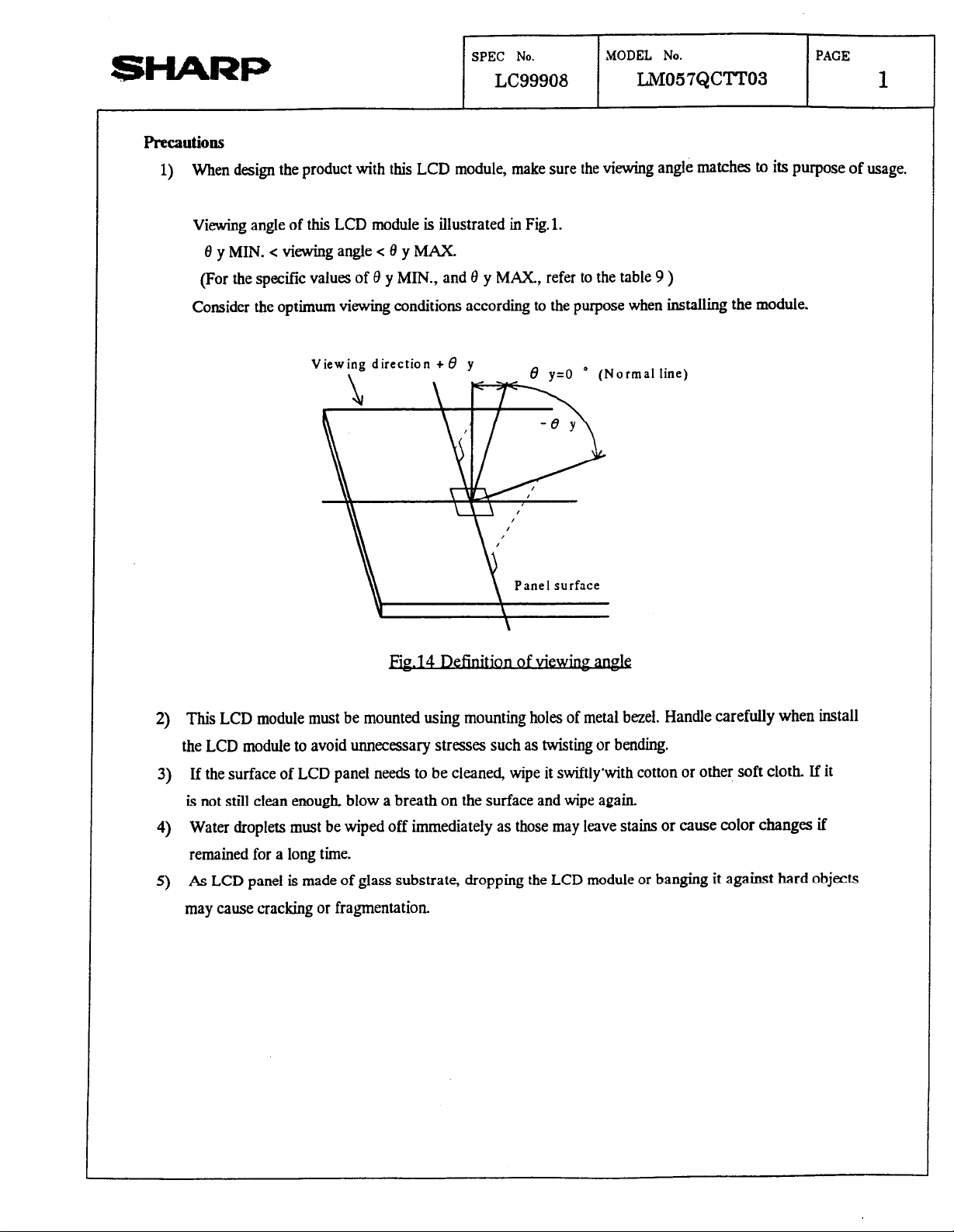
1) When design the product with this LCD module, make sure the viewing angle matches to its purpose of usage.
Viewing angle of this LCD module is illustrated in Fig. 1.
8yMIN.<viewingangle<OyMAX.
(For the specific values of 6 y MIN., and 8 y MAX., refer to the table 9 )
Consider the optimum viewing conditions according to the purpose when installing the module.
SPEC No.
LC99908
MODEL No.
LM057QClT03
I
PAGE
1
I
Viewing direction + 6
Ei~-14 Definttlonofwe~
2) This LCD module must be mounted using mounting holes of metal bezel. Handle carefully when install
the LCD module to avoid unnecessary stresses such as twisting or bending.
3) If the surface of LCD panel needs to be cleaned, wipe it swiftly’with cotton or other soft cloth If it
is not still clean enough, blow a breath on the surface and wipe again
y
Panel surface
. . . .
ormal line)
4) Water droplets must be wiped off immediately as those may leave stains or cause color changes if
remained for a long time.
5)
As LCD panel is made of glass substrate, dropping the LCD module or banging it against hard objects
may cause cracking or fragmentation.
Page 4
@HARP
6) As CMOS LSIs are equipped in this module, following countermeasures must be taken to avoid
electrostatics charges.
1. Operator
Ware the electrostatic shielded clothes because human body may be statically charged if not ware shielded
clothes.
2. Equipment
I I
SPEC No. MODEL No.
LC99908
LM057QCTT03
I
PAGE
2
There is a possibiiity that the static electricity is charged to the equipment which have a function of
or friction action(ex: conveyer, soldering iron, working table). Earth the equipment through proper
resistance(electrostatic earth: 1 X 10” 9).
3. Floor
Floor is the important part to drain static electricity which is generated by operators or equipment.
There is a possibility that charged static electricity is not properly drained in case of insulating floor.
Set the electrostatic earth(1 X lO”S2).
4. Humidity
Proper humidity helps in reducing the chance of generating electrostatic charges. Humidity should be kept
over 50%RH.
5. Transportation/storage
The storage materials also need to be anti-static treated because there is a possibility that the human body or
storage materials such as containers may be statically charged by friction or peeling.
6. Others
The laminator@rotective film) is attached on the surface of LCD panel to prevent it from scratches or stains.
It should be peeled off slowly using static eliminator.
Static eliminator should also be installed to the work bench to prevent LCD module from static charge.
7) Do not use any materials which emit gas from epoxy resin(hardener for amine) and silicone adhesive
peeling
agent(dealcoho1 or deoxym) to prevent discoloration of polarizer due to gas.
8) The brightness of the LCD module may be affected by the routing of CCFI cables due to leakage to the
chassis through coupling effect. The inverter circuit needs to be designed taking the level of leakage current
into consideration. Thorough evaluation is needed for LCD module and inverter built into its ho& equipment
to ensure specified brightness.
9) Avoid the exposure of the module to the direct sun-light or strong ultraviolet light for a long time.
10) If the LCD module is stored at below specified temperature, the LC material may freeze and be deteriorated
If it is stored at above specified temperature, the molecular orientation of the LC material may change to
Liquid state and it may not revert to its original state. Therefore, the LCD module should always be stored
within specified temperature range.
11) Disassembling the LCD module can cause permanent damage and it should be strictly avoided
Page 5
@HARP
12) Procedure to insert mating connector
SPEC No.
LC99908
MODEL No.
LM057QCTT03
PAGE
3
When the mating connector is inserted, it should be parallel to the connector on the
should be inserted horizontally. Do not leave a gap beh>een two connectors.
13) The module should be driven according to the specified ratings to avoid malfunction and permanent damage.
Applying DC voltage causes a rapid deterioration of LC material. Make sure to apply alternating waveform
by continuous application of the M signal. Espe&&& power ON/OFF sm 17 &n&l&
t to avov DC m
14) LCD retains the display pattern when it is applied for long time.(Image retention)
To prevent image retention. do not apply the flied pattern for along time.
15) Image retention is not a deterioration of LCD. It will be removed after display pattern is changed
16) CCFI’ backlight should be kept OFF during VDD is “L” level.
Precautions for touch panel
1) Designing
1. Active area
Active area is defined as input area by pen or finger. Its function, optical properties and durability
LCD
module and it
are specified in the specifications.
a) Detection of coordinates and calbration must always be conducted within active area. If those are
conducted outside of the active area, those may cause functional errors.
b) Area which is actually accessed by pen or finger must be designed within active area. If it is
designed outside of the active area, it may cause functional error.
2.Neutral area
Neutral area is located around the active area for l.Omm wide. Although the coordinates can be detected
in this area, its functionality, optical properties and durability are not assured.
a) Neutral area detects coordinates when input by pen or finger, but it may cause functional error
when it is treated as detected data.
b) As the purpose of the neutral area is to protect inactive area, pushing hardly by pen tip or others
may cause deterioration of its durability.
3.Visible area
This is transparent area where silver electrode or flex printed with opaque ink are not existing.
It assures qualities related to appearance standards defined in the specifications.
4Jnactive area
Upper electrode or lower electrode in the inactive area is printed with transparent insulation ink on it.
It is located outside of the active area and a non functional area.
a) Inactive area is printed with insulation ink. Hard push action may cause a deformation of upper
electrode film and may lead to a malfunction in the active area nearby. Upper electrode may come
J
Page 6
@HARP
b) As the purpose of the inactive area is to keep the flatness of the upper electrode ftirn in the touch panel
Designing print circuit
1. There is a contact resistance between upper and lower electrodes of the touch panel. It is recommended
to set the impedance of detecting circuit high enough. Low impedance detecting circuit may cause a
functional error.
2. Contact of the upper and lower electrode generates a contact resistance. Access by pen or finger to the
touch panel should be started after the contact resistance becomes stable. Otherwise, it may cause
a functional error.
3. Touch panel picks up a noise easily. It is recommended to earth or do other noise protections. Otherwise,
it may cause a functional error.
r I
SPEC No.
MODEL No. PAGE
LC99908 LM057QCTT03
in contact with lower electrode and may cause a electrical leakage.
structuie. hard push by pen or by system chassis may cause a functi&al error.
I
4
Designing system chassis
1. Retain the air gap between upper electrode film and front chassis.
a) Retain minimum of 0.3mm air gap above the inactive area so that the front chassis does not make a
pressure on upper electrode film. If there is any pressure on it, it may cause a functional error due to
the deformation of the upper electrode film.
b) Flexible material such as rubber is recommended as cushioning materials. It should be placed outside of
visible area. If it is placed onto inactive area, it may cause a functional error due to deformation of
the upper electrode film.
2. Assemble design
a) Do not glue nor tape system front chassis to the surface of touch panel(upper electrode fam) as it may
lead to peeling off of the upper electrode film
b) Make sure not to swell the upper electrode film by atmospheric pressure difference between inside and
outside of the system. If it is swelled, it may cause a deterioration of durability of the touch panel and
may cause a functional error.
c) Prevent vapor condensation to the touch panel. Do not expose the touch panel to high humidity
Atmosphere, vaporous air, or to any liquid such as water. It may cause a leakage inside the touch panel
structure:
Upper electrode film and lower electrode glass are fied by adhesive, and there is a ventilation hole
between film and glass. Liquid penetrate into touch panel easily due to this structure. Design the system
carefully so that liquid will not penetrate into touch panel.
Page 7
SHARP
Assembling LCD module with touch panel
* 1. Unpacking
SPEC No.
LC99908
a) Do not hold nor pull flex cable. otherwise it may cause a breakage of the flex.
b) Glass edge of touch pane1 is not treated It is sharp edge and it may cause an injury when handled
by bare hands. Wear finger sacks or groves and handle with extra care.
2. Handling
a) Do not pick up the visible area or flexible tail.
b) Do not stack up the LCD module. Do not place anything on the LCD module. It may cause scratch,
deformation or breakage.
c) Wipe a dirt on the screen with dry soft cloth If it is still sticked, wipe it out with soft cloth with
ethyl alcohol. Upper electrode film and lower electrode glass of touch panel are fixed by adhesive
and there is a ventilation hole in between. Be careful not to have ethyl alcohol may penetrate into
touch panel. It may cause a functional error.
iMODEL No. PAGE
LM057QCTT03
5
3. Assembling
a) Be careful not to apply excessive distortion on heat sealed area of the flex cable. It may cause a
functional error.
b) Be careful not to scratch the front of touch pane1 during assembly process.
4. Operating instruction
a) Use a finger or a polyacetal pen to access to touch panel. The surface of the touch panel film
is hard coat treated. This hard coating may be damaged if it is touched by a ball-point pen or
metal piece.
b) Do not expose the LCD module to the direct sun-light for long period of time. Polyester film is
used as the front film of the touch panel, exposure to direct sun-light for long time may cause
a discoloration
c) If a chemical material stays on the touch panel for long period of time, front film may be swelled
and may cause a functional error. If it is planned to be used under severer circumstances, very
careful protection is required
Page 8
SHARP
SPEC No. MODEL No. PAGE
LC99908 LM057QCTI'03
6
OContents
1. Application
2. Construction and Outline
3. Mechanical Specifications
4. Absolute Maximum Ratings
5. Electrical Specifications
6. Module driving method
7. Optical Characteristics
8. Characteristics of Backlight
Page
7
7
7
15
17
20
9. Touch panel specification
10. Supply voltage sequence condition
11. Outline dimension
21
22
23
Page 9

SPEC No.
SHARP
l.Application
This data sheet is to introduce the specification of LM057QCTT03,negative Matrix type Color LCD module.
2.Construction and Outline
Construction: Touch panel and 320 X RGB X 240 dots color display module consisting of an LCD panel,
PWB@rinted wiring board) with electric components mounted, TCP(tape carrier package) to connect the LCD panel
and PWB electrically, and plastic chassis with CCFT’ back light and bezel to hold them mechanically. Signal
ground(Vss) is connected with the metal bezel.
PUB
TCP
LC99908
LCD Panel
MODEL No.
'LM057QCTT03
Touch panel Bezel
PAGE
/
7
II /
-WI
I -
I I /
B? /
Application inspection standard
The LCD module shall meet the following inspection standard :
3.Mechanical Specification
Parameter Specifications
Outline dimensions *l
Viewing area 118.2(W) X 89.4(H)
1
-G&J-
Outline :See Fig. 13
Connection :See Fig. 13 and Table 6
154.6+0.5(W) x 114.8*0.5(H)x 9. 85*0.7(D)
Light pipe
,
I
0
fl
CCPT /
unit
nlm
nun
Active area 115.18(W) X86.38(H)
Display format
Dot size
Dot spacing 0.02
Base color *2
Mass
*1 Due to the characteristics of the LC material, display colors may vary with ambient temperature.
*2 Negative-type display
Display data “H” -+ Display ON = white
Display data “L” -+ Display OFF = black
320 X RGB(W) X240(H)
0.1 X RGB(W) X0.34(H)
Normally black
Approx. 250
mm
mm
mm
t3
Page 10

@HARP
4. Absolute Maximum Ratings
ClXlectrical absolute maximum ratings
4-2Xnvironment Conditions
Ambient temperature , humidity conditions
SPEC No.
LC99908
MODEL No.
LM057QCTT03
PAGE
8
Item
Ambient temperature
Humidity Note 2)
Note 1)
Note 2) Tas40 “c . . . . . . . 95 % RI-I Max.
Vibration conditions
The display module should not be operated nor stored outside of specified temperature
range.
Ta>40 “c . . . . . ..Absolute humidity shall be less than Ta=40 “C/95 % RI-I.
Frequency 10 Hz-57 Hz 57 Hz-500 Hz
Vibration level 9.8 m/s’
Vibration width 0.075 mm
Interval 10 Hz-500 Hz-10 HGl.0 min
2 hours for each direction of XN/Z (6 hours as total)
Topr
MIN. MAX. MIN. MAX.
0 “C
+50 “c
-25 “c
Tstg
Remark
+6O”C Note 1)
No condensation
Shock conditions
Acceleration : 490 m/s’
Pulse width : 11 ms
3 times for each directions of * X/ + Y/t Z
Page 11

SHARP
5. Electrical Specifications
5-l.Electrical characteristics
Supply voltage (LCD)
SPEC No.
MODEL No.
LC99908 LM057QCTT03
PAGE
9
Note 1) Frame frequency = 75 Hz.
Note 2) Frame frequency = 75 Hz V,, - Vss = 26.1V, V,, = 5 V
Display pattern = checker flag pattern
1 2
3 4 . . . . . . . . . . . . . . . . . . . . . . . . . . . . . . . . . . . . . . . . . . . gfjo
1
2
3
.
239
240
Note 3) Except Lamp power consumption. (*See Page 20)
clm0mclmclm0mcim0m0wclmclm
n amclm0mclB0m0m!Jmnm0mcl
q m0mclmclm0mclm0m0mclm0m
¤omnmam0m0m0mnm~a0m0
clmclm0mumclmclmlJm0BiJBclm
n nm0mc!mclmciB0m0m0mclmcl
Page 12

Supply voltage (LCD)
Iuput signal voltage
Note 1) Frame frequency = 75 Hz.
SPEC No.
LC99908
MODEL No.
LM057QC'I"l!03
PAGE
10
Note 2) Frame frequency = 75 Hz, V,, - Vss = 26.1V, V,,, = 3.3V
Display pattern = checker flag pattern
1234
1 lJm0m0mclm0mclmamclmc!mclm
2
3
.
239
240
Note 3) Except Lamp power consumption. (*See Page 20)
n
0m0m0m0m3m3mnmnmamn
q
m0mnm0m0m0mnmamnm0m
n
0mnm0m0mnmamum0m0m0
q
m0mnm~m0m0m0mnmnmam
¤0mnm0m0m0mnm0mnm0m~
. . . . . . . . . . . . . . . . . . . . . . . . . . . . . . . . . . . . . . . . . . .
960
Page 13

SHARP
. .
5-2 Interface signals
0 LCD
SPEC No.
LC99908
MODEL No.
LM057QCTT03
PAGE
11
Display data signal
0 CCFT e 7 CN? tCCFQ
No. Symbol Description
1
2 NC
3
OTO
:
VLl(HV)
VL2(GND)
High voltage line(fiom Iuverter)
Ground line(from Inverter)
“H” (ON), “L”(Oq
Note
for back light
Used connector
CNl : 53216-1510
CN2 : BHR-03VS-1
CN3 : FPC Ag/C Conductor
Correspondable connector
CNl : 51021-1500
CN2 : SM02-(8.0)B-BHS-1
CN3 :SFWJR-5STE
(Display functions and reliabilities are not guaranteed for the usage of unspecified mating connectors.)
(M0I-W
(‘S-4
(MO=9
(‘ST)
WI)
Page 14

SHARP
53.Interface timing
SPEC No.
LC99908
LP ’ ‘40 pulses >r
//
N
MODEL No.
LA4057QCTT03
PAGE
12
DO
1” line’s
data
I I
2” line’s
data
XCK
nnr
l
320 *(3/g) oulses
FiP 7
COLUMN
------------------------
Tnterface tlm InP
. .
7
I
1
(240,l) (240,2)
320 x 3(RGB)
x 240 dots
Fig.3 Dot chart of disDlav area
(2,319) (2,3 0):
(240,319) (240,320)
4 ,
Page 15

SHARP
SPEC No.
LC99908
iMODEL No.
PAGE
LMO57QCTT03
Ta=25 “C,VDD = 5.0 Vr5 %(3.3V t5 %)
13
XCK 1 allowance time from LP f
Input
signal rise/fall time*1
Note 1) Due to the characteristics of the LCD module, “shadowing” effect becomes more visible as frame
refresh frequency goes up. And also contrast ratio goes down and flickering becomes more visible as
flame refresh frequency goes down. It is recommended to drive the display module according to
the specified conditions.
Recommended frame refresh frequency range is 70 Hz- 80 Hz.
Note 2)LP signal must be continuous. And also its interval time from the falling edge to the rising edge must
always be same and no greater than 70 cr s.
tLH
t,*tr
200 - - lx3
- -
13 ns
Page 16

SHARP
SPEC No.
LC99908
MODEL No.
LM057QCTT03
PAGE
14
YD -
LP
xc
t
WLPH
< >
r
t
7
tr
t
<
LS
>
t
<
LH
\ /
/ \
CK
<
tWCKH tWCKL
I
DO-7
VIH= 0. av,,
v,, = 0. zv,,
Fig.4 Interface timing chart
Page 17

SHARP
1
6. Module Driving Method
6-1. Input data’and control signal
One SEG(segment=column)driver is a 240 bit output LSI, consisting of shift registers, latch circuits and
LCD driver circuits.
Input data for each row (320 X 3[R,G,E?]) will be sequentially transferred in the form of 8 bit parallel
data through shift registers by data transfer clock signal (XCK). When data transfer for one row (320 X
3[R.,G,B]) is completed, the data will be latched in the form of 320 x 3 parallel data corresponding to each
column electrodes by the falling edge of latch signal (LP), then the drive pulses will be output to 320 X 3
lines of column electrodes of the LCD panel by the LCD drive circuits.
At the same time. row N is selected by scan start-up signal (YD) and the contents of the data signals are
displayed on the row N of the display screen according to the combinations of voltages applied to row and
SPEC No.
MODEL No.
LC99908 LM057QCTT03
PAGE
15
/
8
column electrodes. While the data row N are being displayed, data for row N+l are transferred After 320 X 3
data have been transferred, data will be latched by the falling edge of LP and output the data to the row N+l.
Bach row will be sequentially selected as described above from N=l to N=240. One frame is completed
after displaying 240”’ row. Then row scan starts from the 1st row again YD is the scan signal which drives
row electrodes.
If DC voltage is applied, it causes a chemical reaction in LC material and causes a deterioration of LC
material. So, the polarities of driving pulses must be alternated by certain time period. Control signal M is
the signal which changes the polarity of driving pulses.
Power consumption of the LCD module goes up as clock(XCK) frequency goes up due to the nature of
CMOS LSI used in it. This display module has 8 bit parallel data input so that it works at low clock frequency
and rninin&e power consumption. 8 bit display data are assigned to DO-7.
This display module also has a bus line system for data input to
of each LSI driver works only when data is accessed
minimize the power consumption. Data input
Data Input for column electrodes and Chip Select of driver LSI work as follows:
The driver LSI at the left end of the screen is selected first and 240 bits of data(30 x XCK) are transferred to itAfter transferring 240 data, the adjacent right side LSI right is selected. This process is sequentially continued
until data is fed to the LSI at the right end of the screen. Thus display data is transferred sequentially through
8 bit bus line from the left to the right of the screen.
Page 18

SHARP
As this display module does not have display refresh RAM, display data and timing control signals must
be supplied continuously.
The timing chart of input signals are shown in Fig. 4 and Table 9.
SPEC No.
LC99908
MODEL No.
LM057QClT03
PAGF;
16
Page 19

SHARP
7. Optical Characteristics
SPEC No. iMODEL No.
LC99908 LM057QCTT03
PAGE
17
Contrast ratio co
Response Rise r
time
Brightness B
Module
chromaticity Y
Decay rd
X
white
r
e,=ey=o
e
x=e,=o o 25 40 _.
e,=e,=o
e
x=e,=o o
0 JL =
e,=e,=o
e .=e,=o
0
-
6.0 mA 120 1.50 o 0.28 0.33 0.38
o
0.29 0.34 0.39
450 600 ms
100 130 ms
- Note2)
Note3)
cd/m’ Note4)
-
-
tey
.
tex
-eY
of View
Note 1) The viewing angle range is defmed as shown Fig.5
Note 2) Contrast ratio is defined as follows:
co Luminance(
Luminance( brightness) of all pixels ” Dark ” at Vmax
Vmax is defined in Fig.7.
Note 3) The response speed of LCD module is defined as the response characteristics of photo-detector output
shown in Fig.6 when the measured dot is turned on and off in the setting shown in Fig.8
No&)
Luminance is defined as average luminance (brightness) of measuring points (a>-@)
All pixels of LCD are “white’.
brightness) of all pixels “White” at Vmax
-eY
at Vmax.
Page 20

SHARP
SPEC No.
LC99908
MODEL No.
LM057QCTT03
Co
max
PAGE
18
I
-
te
Measuring Spot Size : 4 10 mm
8x:
Angle from “normal” to measuring direction along the horizontal axis.
Angle from “normal” to measuring direction along the vertical axis.
By:
Fig.6 Optical Characteristics Test Method I
(Response Speed Measurement)
Ta = 25 “C
In the dark room
Field: 2 ’
TOPCON BM7 + quartz fiber
(Measuring spot size : 9 10 mm, Measuring Field : 2 ’
e
Y(+),,
L/
Vma x
Fig.7 Definition of Vmax
Vbl t age
)
)
LCD Module
80 mm
\
Fie. 8 Outical Characteristics Test Method D[
\ /
Computer
I
Page 21

SHARP
SPEC No.
LC99908
l/240 D uty Ratio
MODEL No.
LM057QCTT03
PAGE
I
19 i
XCK
nn- 7
YD
. . .
efrnttlon
rr: Rise time
rd: Decay time
4
SEG Drv.
CCFT
Inverter
L I
X+,Y+.X-,Y- Touch panel
*Signal ground(Vss)
.lO Circuit block diaorm
is connected with the metal
Page 22

&iARP
8.Characteristics of Backlight
The ratings are given on condition that the following conditions.
1) Rating(Note)
SPEC No.
LC99908
I
MODEL No.
LM057QClT03
I
PAGE
I
20
/
Parameter MIN.
L Brightness 120
TYP. MAX
150
2) Measurement circuit : CXA-MlOL(TDK) (at IL = 6.0 m4rms)
3) Measurement equipment : BM-7 (TOPCON Corporation)
4) Measurement conditions
4-l. Measurement circuit voltage : DC = 12.OV,
at primary side
4-2. LCD: AI1 digits WHITE, Vat,= 5.0 V(3.3V), V,, = Vmax, D7-0 :“H”(White)
l/tFRM = 75 Hz
4-3. Ambient temperature : 25 “C
Measurement shall be executed 30 minutes after turning on.
5)
5-l. Rating (lpc)
unit
cd/m’
*1 It is recommended that IL is no greater than 6 mArms so that the effect of heat radiation from CCFT
backlight on display quality is minimized
*2 Power consumption excluded inverter efficiency loss.
*3 The output voltage of the inverter should be set to Vs adding some margin as Vs of CCFT bulb may
be increased due to AC coupling leakage to the chassis of the LCD module.
*4 Average life time of CCFT bulb will be decreased when LCD is operated at lowtemperature.
Page 23

SPEC No.
SHARP
6) Operating life
The operating life time is 25 000 hours or more at 6 mArms, 25 + 1°C
(Operating life with CXA-MlOL or quivalent.)
The inverter should meet the following conditions to keep the specified life time of used lamp;
-Sine wave form, symmetric in positive and negative, no ripple or spike pulse
-Output frequency range: 4Oh-80 kH2
Check well that CCFT works properly with enough aging time.
The operating life time is defined as the time either of following conditions are met.
-When the luminance or amount of light output is decreased to 60 % of the initials value.
-When the kick-off voltage reaches Maximum value in Table 11.
(NOTE) Ratings are defined as the average brightness inside the viewing area specified in Fig.11.
LC99908
MODEL No.
LM057QCTT03
PAGE
21 I
60
180
dots
I
80 160
I
I
240 dots
(l-5)
Activation Finger -
Stylus -
Surface hardness 2H - - -
Optical clarity so -
0.5
0.5
N
N
%
Page 24

SHARP
10. Supply voltage sequence condition
The power ON/OFF sequence shown on Fig. 12 must be kept to avoid latch-up of driver LSI and
DC voltage charge to LCD panel.
V
DD
YD
LP
XCK
DATA
SPEC No.
IX99908
500 ms MIN. (Note 1)
rMODEL No.
LM057QCTT03
PAGE
22
DISP
VEE
POWER ON POWER OFF
Symbol
a OmsMIN.
Allowable value Symbol Allowable value
1sMAx.
b 20 ms MIN.
c . 100 11s MAX
d
0 ms MIN.
Se-n
-+-i-
. .
f
g
h
0 ms MIN. 1SMAX.
20msMIN.
20 ms MIN.
i 0 ms MIN.
e 0 ms MIN.
Note
1)
Power ON/OFF
cycle time. All signals and power lines must be switched in
sequence during power ON/OFF cycle.
accordance with above
Page 25

5. 3to.5 _I &
I ,_ 4. 05to.s
II I-
;;d
ml;;
I I
n 1
MOUt NO
PAGE
908 d57QCTT03 23
IY5tY
INTERFACE CONNECTOR
2-4
8.9 ‘_ 118.4 Mirr 1111 (l/p)
7. 5 121. 2 ; litllllllf~i IT/p)
I 12. 5 131. 7+0 3 I Clils llllihl IT/P) _
m
x
I 10 I I 3. CCFT CO CTOR : BHR-03~S-1 (JST)
1. 3(CNl)
I
BF7FL OPENNIG ARFA
-+/
J
1 1 TOLERANCE X-DIRECTION A 3. 21*0. 5
2) TOLERANCE Y-DIRECTION E 3. lr*O 5
3) OBLIQUITY OF DISPLAY AREA IC-DICO.5
iI /
I
I I
im i0
t
ACTIVE ARFA
I
AUKI amm
CCFT CONNECTOR
T/P CONNECTOR
UL3567 AWG26
0 TOL TO BE to. 5
: 53261-:SlO~MOLEX)
LCD MODU!E
OUTLINE DIMENSiON'
 Loading...