

Page 1
3Axis - 2g/6g LINEAR ACCELEROMETER
■ 3V TO 5.25V SINGLE SUPPLY OPERATION
■ THE SENSITIVITY IS ADJUSTED WITH A
TOTAL ACCURACY OF ±10%
■ THE OUTPUT VOLTAGE, OFFSET,
SENSITIVITY AND TEST VOLTAGE ARE
RATIOMETRIC TO THE SUPPLY VOLTAGE
■ DEVICE SENSITI VITY IS ON-CHI P FACTORY
TRIMMED
■ EMBEDDED SELF TEST
■ HIGH SHOCK SURVIVABILITY
DESCRIPTION
The LIS3L02AQ is a three-axis linear accelerometer that includes a sensing eleme nt and an IC interface able to take the information from the
sensing element and to provide an analog signal
to the external world.
The sensing element, capable to detect the acceleration, is manufactured using a dedicated process called THELMA (Thick Epi-Poly Layer for
Microactuators and Accelerometers) developed
by ST to produce inertial sensors and actuators in
silicon.
The IC interface instead is manufactured us ing a
CMOS process that allows high level of integration
to design a dedicated circuit which is trimmed to
better match the sensing element characteristics.
The LIS3L02AQ has a user selectable full scale of
LIS3L02AQ
INERTIAL SENSOR:
PRODUCT PREVIEW
QFN-44
ORDERING NUMB ER: LIS3L 02AQ
2g, 6g and it is capable of measuring accelerations
over a maximum bandwidth of 4.0 K Hz for the X
and Y axis and 2.5KHz for the Z axis. The device
bandwidth may be reduced by using external capacitances. A self-test capability allows the user to
check the functi o n ing of th e syst e m.
The LIS3L02AQ is available in plastic SMD package and it is specified over a temperature range
extending from -40°C to +85°C.
The LIS3L02AQ b elongs to a fam ily of products
suitable for a variety of applications:
– Antitheft systems
– Inertial navigation
– Virtual reality input devices
– Vibration Monitoring, recording and com pen-
sation
– Appliance control
– Robotics
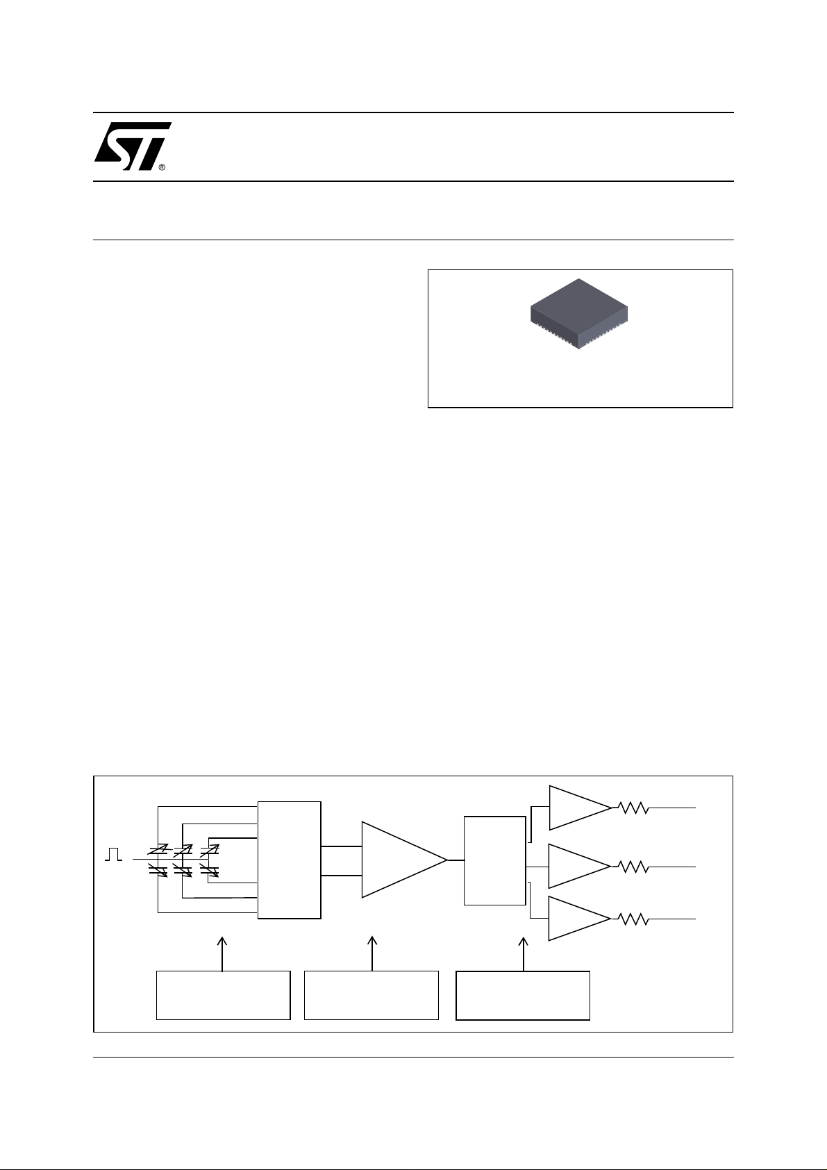
BLOCK DIAGRAM
S1X
S1Y
S1Z
rot
S2Z
S2Y
S2X
VOLTAGE & CURRENT
REFERENCE
February 2003
This is preliminary information on a new product now in development. Details are subject to change without notice.
MUX
TRIMMING CIRCUIT
TEST INTERFACE
AMPLIFIE R
DEMUX
CLOCK
&
PHASE GENERATOR
S/HCHARGE
S/H
S/H
&
Routx
Routy
Routz
Voutx
Vouty
Voutz
1/7
Page 2
LIS3L02AQ
PIN DESCRIPTION
N° Pin Function
1 to 3 NC Internally not connected
4 GND 0V supply
5 Vdd Power supply
6 Vouty Output Voltage
7 ST Self Test (Logic 0: normal mode; Logic 1: Self-test)
8 Voutx Output Voltage
9-13 NC Internally not connected
14 PD Power Down (Logic 0: normal mode; Logic 1: Power-Down mode)
15 Voutz Output Voltage
16 FS Full Scale selection (Logic 0: 2g Full-scale; Logic 1: 6g Full-scale)
17-18 Reserved Leave unconnected
19 NC Internally not connected
20 Reserved Leave unconnected
21 NC Internally not connected
22-23 Reserved Leave unconnected
24-25 NC Internally not connected
26 Reserved Connect to Vdd or GND
27 Reserved Leave unconnected or connect to Vdd
28 Reserved Leave unconnected or connect to GND
29-44 NC Internally not connected
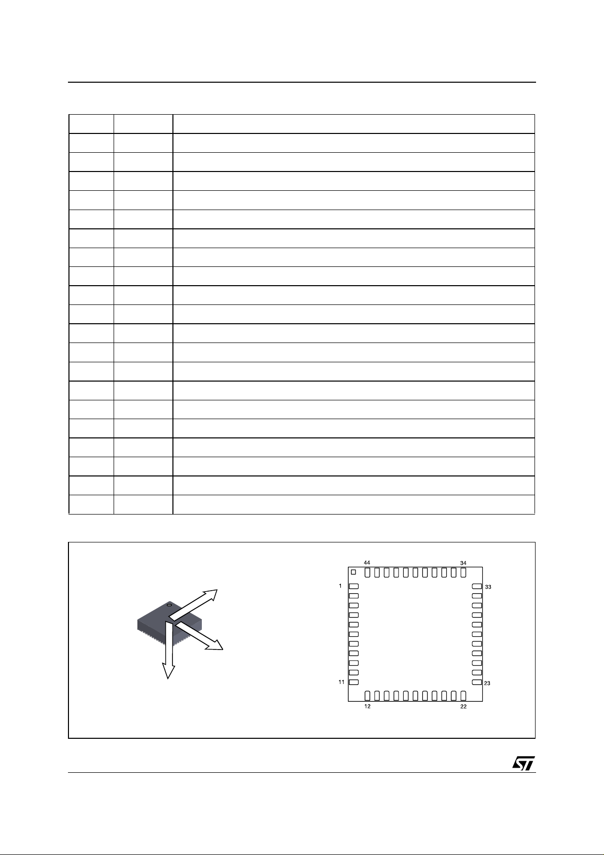
PIN CONNECTION (Top view )
1
Z
Y
X
DIRECTION OF THE
DETECTABLE
ACCELERATIONS
GND
Vdd
Vouty
Voutx
NCNCNCNCNCNCNCNCNCNCNC
NC
NC
NC
LIS3L02AQ
ST
NC
NC
NC
FS
PD
NC
NC
Voutz
Reserved
Reserved
Reserved
ReservedNCReserved
NC
NC
NC
NC
NC
Reserved
Reserved
Reserved
NC
NC
Reserved
2/7
Page 3

LIS3L02AQ
ELECTRICAL CHARACTERISTCSS(Temperature range -40°C to +85°C)
Symbol Parameter Test Condition Min. Typ. Max. Unit
Vdd Supply voltage 3 5.25 V
Idd Supply current 1.0 mA
Voff Zero-g level T = 25°C
ratiometric to Vdd
Ar Acceleration range 0V on FS pin ±1.8 ±2.0 ±2.2 g
Vdd on FS pin ±±6.0 g
So Sensitivity ratiometric to Vdd T = 25°C
NL Non Linearity Best fit straight line
fuc Sensing Element Resonant
Frequency
an Acceleration noise density Vdd=5V
Vt Self test output voltage
Ratiometric to Vdd
Vst Self test input Logic 0 level 0 0.8 V
Full-scale = 2g
T = 25°C
Full-scale = 6g
X, Y axis
Full-scale = 2g
Best fit straight line
Z axis
Full-scale = 2g
X, Y axis 4.0 KHz
Z axis 2.5 KHz
Full-scale = 2g
T = 25°C
@ 5V
Vdd/2-10% Vdd/2 Vdd/2+10% V
Vdd/5–10% Vdd/5 Vdd/5+10% V/g
Vdd/15–10% Vdd/15 Vdd/15+10% V/g
±0.3 %
±0.6 %
100
TBD V
µg/
Hz
Logic 1 level 2.8 Vdd V
Rout Output impedance 100
Cload Capacitive load drive 320 pF
kΩ
1 FUNCTIONALITY
1.1 Sensing element
The THELMA proces s is utilized to c reate a surfac e micro-mach ined accelerom eter. The technolo gy allows to carry out suspended silicon structures which are attached to the substrate in a few points called
anchors and free to move on a plane parallel to the subst rate itself. To b e com pati ble with the tradi tional
packaging techniques a cap is placed on top of t he sensing element to avoi d blockin g the moving p arts
during the molding phase.
The equivalent circuit for the sensing element is shown in t he below figure; when a linear acceleration is
applied, the proof mass di splaces from its nominal po sition, c ausing an imbalance in t he cap acitive hal fbridge. This imbalance is measured using charge integration in response to a voltage pulse applied to the
sense capacitor.
The nominal value of the capacitors, at steady state, is few pF and when an acceleration is applied the
maximum variation of the capacitive load is few tenth of pF.
3/7
Page 4

LIS3L02AQ
Figure 1. Equivalent electrical circuit
C
ps1
R
s1
S1x
C
C
pr
s1x
R
r
C
s2x
S2x
C
ps2
C
ps1
R
s2
R
s1
S1y
C
C
pr
s1y
R
r
rot
C
s2y
S2y
C
ps2
C
ps1
R
s2
R
s1
S1z
C
C
pr
s1z
R
r
C
s2z
S2z
C
ps2
R
s2
1.2 IC Interface
The complete signal processing uses a fully differential structure, while the final stage converts the differential signal into a single-ended one to be compatible with the external world.
The first stage is a low-noise capacitive amplifier that implements a Correlated Double Sampling (CDS) at
its output to cancel the offset and the 1/f noise. The produced signal is then sent to three different S&Hs,
one for each channel, and made available to the outside.
The low noise input amplifier operates at 200 kHz while the three S&Hs operate at a sampling frequency
of 66 kHz. This allows a large oversampling ratio, which leads to in-band noise reduction and to an accurate output waveform.
All the analog parameters (output offset voltage and sensitivity) are ratiometric to the voltage supply. In-
4/7
Page 5

LIS3L02AQ
creasing or decreasing the voltage supply, the sensitivity and the offset will increase or decrease linearly.
The feature provides the c ancel lat ion of the error rel ate d to t he voltage supply alo ng an analog to digital
conversion chain.
1.3 Factory calibration
The IC interface is factory calibrated to provide to the final user a device ready to operate. The parameters
which are trimmed are: gain, offset, common mode and internal clock frequency.
The trimming values are stored inside the devi ce by a poly-fuse structure. Any t ime the device is turned
on, the memorized bits are downloaded into the registers to be employed during the normal operation. The
poly-fuse approach allows the final user to utilize the device without any need for further calibration
5/7
Page 6

LIS3L02AQ
mm inch
DIM.
MIN. TYP . MAX. MIN. TYP. MAX.
A 1.70 1.80 1.90 0.067 0.071 0.075
A1 0.19 0.21 0.007 0.008
b 0.20 0.25 0.30 0.008 0.01 0.012
D 7.0 0.276
E 7.0 0.276
e 0.50 0.020
J 5.04 5.24 0.198 0.206
K 5.04 5.24 0.198 0.206
L 0.38 0.48 0.58 0.015 0.019 0.023
P 45 REF 45 REF
OUTLIN E AND
MECHANI CAL DATA
QFN-44 (7x7x1.8mm)
Quad Flat Package No lead
M
G
M
34
33
23
22
N
44
1
11
12
44
1
DETAIL "N"
SEATING PLANE
DETAIL G
6/7
Page 7

LIS3L02AQ
Information furnished is believed to be accurate and reliable. However, STMicroelectronics assumes no responsibility for the consequences
of use of such information nor for any infringement of patents or other rights of third parties which may result from its use. No license is granted
by implic ation or otherwise under any patent or patent r i ght s of STMi croelectr oni cs. Spec i fications mentioned i n this publication are subject
to change without notice. This publication supersedes and replaces all information previously supplied. STMicroelectronics product s are not
authorized for use as cri tical comp onents in lif e support devi ces or systems without express written approva l of STMicroel ectronics.
The ST logo is a registered trademark of STMicroelectronics
2003 STMicroelectronics - All Ri ghts Rese rved
Austra lia - Brazil - Canada - Chi na - F i nl and - Franc e - Germany - Hong Kong - In di a - Israel - Ita l y - J apan -Malaysia - Malta - Morocco -
Singap ore - Spain - Sw eden - Switze rl and - Unit ed K i ngdom - United States .
STMicroelectronics GROUP OF COMPANIES
http://www.s t. com
7/7
 Loading...