

Page 1
■
HIGH SENSITIVITY 2.5 rad/sec
■
8 BIT A/D CONVERTER
■
800 Hz BANDWIDTH
■
200 rad/sec2 FULL SCALE VALUE
■
DIGITAL DOWNSAMPLING
■
DIGITAL FI LTE R I N G
■
3.3V 3WIRES SERIAL INTERFACE
2
(5V TOLLERANCE)
■
EMBEDDED PLL
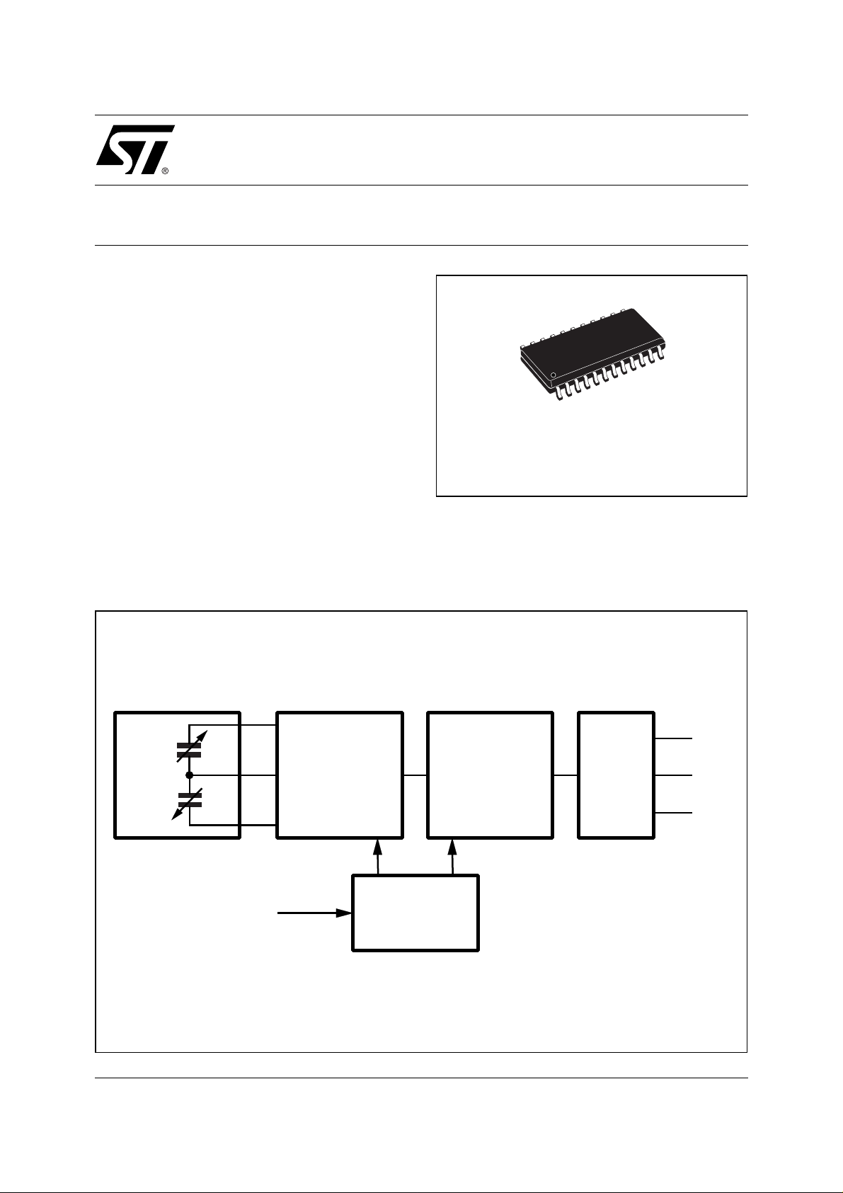
DESCRIPTION
The LIS1R02 is a complete rotational accelerometer
system based on a
Σ∆
architecture, followed by a
digital downsampling block and a digital filter, featuring high sensitivity, 800 Hz signal bandwidth and a
complete serial port interface for a direct connection
LIS1R02 (L6671)
ANGULAR ACCELEROMETER
PRODUCT PREVIEW
SO24
ORDERING NUMBER: LIS1R02
to microprocessor environment. An embedded PLL
allows internal clock generation from an external synchronization signal.
BLOCK DIAGRAM
SENSOR
A/D
CONVERTER
Clk-IN
PLL
DIGITAL
FILTER
SER.
IFC
D02IN1363
SPE
SPD
SPC
April 2002
This is preliminary information on a new product now in development. Details are subject to change without notice.
1/11
Page 2
LIS1R02 (L6671)
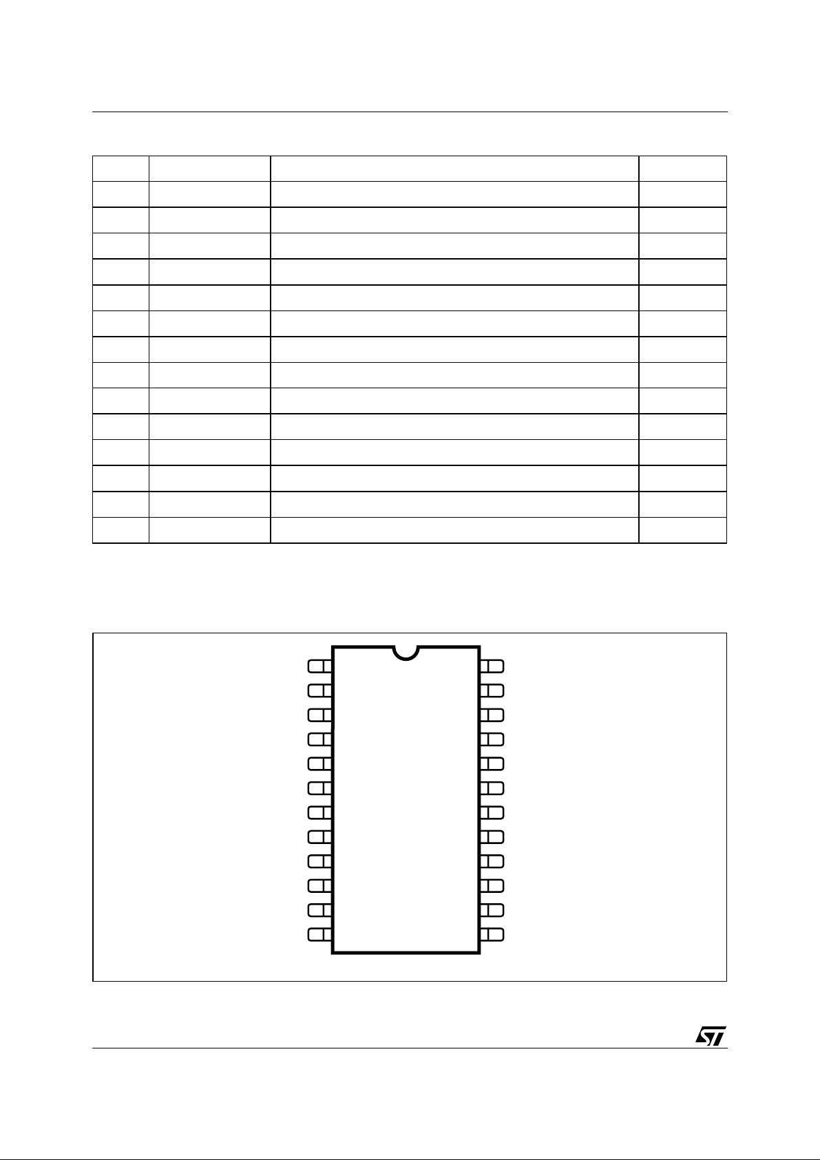
PIN FUNCTION
N°. Pin Name Function Typ. Condition
1 to 6 GND Ground
7 Vdd_Analog Analog Voltage Supply 5V Typ. (*)
8 Ref_Cap Reference Voltage Bypass
9 HV_Eprom EPROM Programming Voltage (test mode only) Tied to GND
10 Vdd_Digital Digital Voltage Supply 5V Typ. (**)
11 SPC Serial Port Clock Signal
12 SPD Serial Port Data Signal
19 to 24 GND Ground
13 SPE Serial Port Enable Signal
14 CLK_In External Clock / PLL Reference Input
15 Gnd_Digital Digital Ground Pin
16 Funct_Test Self Test
17 Test_ST Test Pin Tied to GND
18 Gnd_Analog Analog Ground Pin
(*) Must be shorted to Pin 10
(**) Must be shorted to P i n 7
PIN CONNECTIONS
(Top view)
GND
GND
GND
GND
GND
GND
_ANALOG
V
DD
REF_CAP
HV_EPROM FUNCT_TEST
V
_DIGITAL GND_DIGITAL
DD
SPC CLK_IN11 14
2
3
4
5
6
7
8
9
10
24
23
22
21
20
19
18
17
16
15
GND1
GND
GND
GND
GND
GND
GND_ANALOG
TEST_ST
2/11
1312SPD SPE
D02IN1362
Page 3
LIS1R02 (L6671)
ABSOLUTE MAXIMUM RATINGS
Symbol Parameter Value Unit
Vdd
Vdd
Analog Max
Digital Max
V
in
Maximum analog supply voltage 7 V
Maximum digital supply voltage 7 V
Voltage Range on SPC, SPE, SPD, CLK_In, Funct_Test -0.3 to Vdd
Dig
+ 0.3
ELECTRICAL CHARACTERISTCS
Symbol Parameter Test Condition Min. Typ. Max. Unit
DC
Vdd
Vdd
Idd
Idd
Analog Max
Digital Max
Analog
Digital
V
ref
V
oh
V
ol
V
ih
Analog Supply Voltage 4.5 5.0 5.5 V
Digital Supply Voltage 4.5 5.0 5.5 V
Analog Circuitry Supply Current 15 mA
Digital Circuitry Supply Current 11 mA
Voltage on Ref_Cap pin 2.225 V
(on SPD and Funct_Test) @
= 3mA
I
oh
>2 V
<1 V
2.6 V
V
il
0.8 V
ADC
ADC SNR (30-800Hz, 4.48MHz
35 38 dB
Ext.Clk)
ADC SNR (30-10000Hz,
15 20 dB
4.48MHz Ext.Clk)
Phase error 30-800Hz (relative to a ref.
-30 deg
Accelerometer)
ADC Full Scale 200 rad/
ADC Bandwidth 1-800 Hz
ADC Dynamic Range 38 dB
ADC Differential Linearity <3%
ADC Integral Linearity <5% Full
Mclk Clock Frequency on CLK_In pin 6 MHz
sec
Scale
2
3/11
Page 4
LIS1R02 (L6671)
SERIAL PORT TIMINGS
Symbol Parameter Test Condition Min. Typ. Max. Unit
Pin SPC
Fpc
SPC frequency 25pF maximum load Mclk 30 MHz
Pin SPE
Tec SPE to SPC 5 100 ns
Tce SPC to SPE 5 100 ns
Twe SPE low 1 SPC
Period
Pin SPD (input)
Tds SPD to SPC 5 ns
Tdh SPC to SPD 2 ne
Pin SPD (output)
Tpd SPC to SPD 10 ns
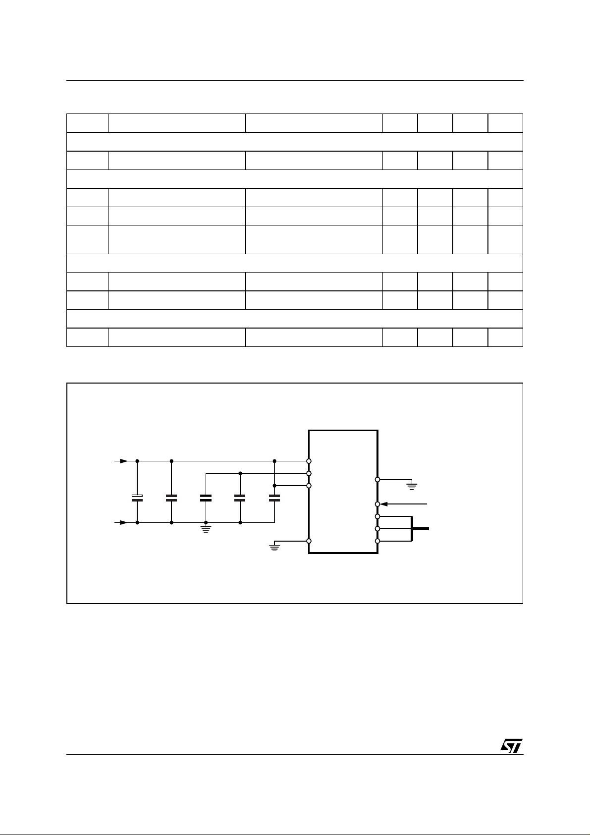
Figure 1. Application Diagram
ns
V
CC
GND
C1
22µF
6V
C2
0.22µF
C3
220pF
C4
0.22µF
C5
0.22µF
7
8
10
1 to 6
9
15 to 24
14
13
12
11
EXTERNAL CLK / PLL REF.
SPE
SPD
SPC
SERIAL I/O
D00IN1118MOD/2
4/11
Page 5

LIS1R02 (L6671)
SERIAL PORT, REGISTERS, EPROM and TEST MODES
1.0 SERIAL PORT
1.1 READ & WRITE REGISTERS
Figure 2.
SPE
SPC
SPD
RW ID2 ID1 ID0 AD3 AD2 AD1 AD0 D7 D6 D5 D4 D3 D2 D1 D0
SPE is the Serial Port Enable. It goes high at the start of the transmission and goes back low at the end. SPC
is the Serial Port Clock. It is stopped high when SPE is low (no transmission). SPD is the Serial Port Data. It is
driven by the falling edge of SPC. It should be captured at the rising edge of SPC.
The Read Register or Write Register command consists of 16 clocks or bit. A bit duration is the time between
two falling edges of SPC. The first bit (bit 0) starts at the first falling edge of SPC after the rising edge of SPE
and the last bit (bit 15) starts at the last falling edge of SPC just before the falling edge of SPE.
■
bit 0 : RW bit. When 0, the data (D7:0) is written into the device. When 1, the data (D7:0) from the device
is read. In this case, the LIS1R02 will drive SPD at the start of bit 8.
■
bit 1-3 : chip ID. The chip ID for the LIS1R02 is ID(2:0)=110. The device accepts the command only
when the ID is valid (equal to 110).
■
bit 4-7 : address AD(3:0). This is the address field for the registers. See section 2 for more details.
■
bit 8-15 : data D(7:0). This is the data that will be written (read) into (from) the register whose address
is AD(3:0).
D00IN1119
1.2 RE A D FI FO
Figure 3.
SPE
SPC
SPD
RW ID2 ID1 ID0 AD3 AD2 AD1 AD0 D7-0 D6-0 ..... D0-0 D7-1 D6-1 ..... D0-1
The Read FIFO command consists of 24 clocks or bits.
bit 0 : READ bit. The value is 1.
bit 1-3 : chip ID. ID(2:0)=110.
bit 4-7 : FIFO address.
bit 8-23: FIFO data.
D00IN1120
5/11
Page 6

LIS1R02 (L6671)
The FIFO has four registers grouped into two banks. The first bank consists of the fi rst and the seco nd register.
The first register is the one written first since the last read. The second bank consists of the third and fourth
register.
0000: address for the first bank
0010: address for the second bank
The device puts out first the data of the first register of the bank with the MSB first.
2.0 LIS1R02 REGISTERS
The registers are grouped into two banks. The following table summarizes their mapping.
Address Reg. Bank 0 Reg. Bank 1
0000 FIFO_Low FIFO_Low
0001 not used not used
0010 FIFO_High FIFO_High
0011 not used not used
0100 CTRL_Reg1 CTRL_Reg1
0101 CTRL_Reg2 CTRL_Reg2
0110 PLL_PRESC_MULT FLASH_Reg1
0111 PLL_MULT FLASH_Reg2
1000 IIR_A0 GAIN_Low
1001 IIR_A1 GAIN_High
1010 IIR_A2 OFFSET_Low
1011 IIR_B1 OFFSET_High
1100 IIR_B2 CURR_BANDGA P
1101 IIR_SIGN_BIT BAND_CSACT_Reg
1110 DSC_Reg CS_TRIM
1111 MISC_Reg MISC_Reg
2.1 Registe rs Bank 0
AD(3:0) = 0100 CTRL_Reg1
This is the first control register. It has 8 bit whose function is summarized below.
Note: x means don't care value.
Note: default value after Power On Reset is 0100 0000
1xxx xxxx Chip in Power Down mode
xx00 xxxx Clock from CLK pin
xx01 xxxx Clock derived from the internal oscillator
xx10 xxxx Clock from the PLL locking on CLK_in
xx11 xxxx Clock from the PLL locking on FIFO_Low reading
xxxx 1xxx Internal Oscillator in Power Down mode
6/11
Page 7

LIS1R02 (L6671)
xxxx x001 Bitstream in mode. The bitstream is sent in via pin Funct_Test while the bitstream clock is sent via
CLK_pin. The output can be checked via the serial interface.
xxxx x010 Bistream out mode. The bitstream is sent out through pin SPD while the bitstream clock is sent
through pin SPC. The pin TEST_ST must be tied to 1.5V.
xxxx x011 Internal clock check mode. The decimation signal is sent out through pin SPD while the main clock
can be checked through pin SPC. The pin TEST_ST must be tied to 1.5V.
xxxx x100 Flash write mode
xxxx x101 Flash read mode
xxxx x11x Sensor trimming
AD(3:0) = 0101 CTRL_Reg2
This is the second control register. It has 8 bit whose function is summarized below.
Note: x means don't care value.
Note: default value after Power On Reset is 0110 0011
0xxx xxxx Delayed Synchronous Conversion reference coming from CLK_pin/FIFO_Low reading signal.
1xxx xxxx Low rate Delayed Synchronous Conversion reference signal.
x1xx xxxx Delayed Synchronous Conversion enabled.
xx1x xxxx Clip on. The result of the measuring chain is clipped when exceding the maximum/minimum limit.
xxx0 0xxx 8 bit output word length
xxx0 1xxx 16 bit output word length
xxx1 xxxx 32 bit output word length
xxxx x1xx Bypass the embedded IIR filter
xxxx xx0x Set the decimation factor to 16. 32 when the bit is 1.
xxxx xxx0 Set the sinc order to 2. 3rd order when the bit is 1.
AD(3:0) = 0110 PLL_PRESC_MULT
This register contain the division factor used in the PLL prescaler and the most significant bit of the PLL multiplication factor.
AD(3:0) = 0111 PLL_PRESC_MULT
This register contain the least significant bit of the PLL multiplication factor.
AD(3:0) = 1000 IIR_A0
This register contain the A0 coefficient used in the embedded IIR register.
AD(3:0) = 1001 IIR_A1
This register contain the A1 coefficient used in the embedded IIR register.
AD(3:0) = 1010 IIR_A2
This register contain the A2 coefficient used in the embedded IIR register.
AD(3:0) = 1011 IIR_B1
This register contain the B1 coefficient used in the embedded IIR register.
7/11
Page 8

LIS1R02 (L6671)
AD(3:0) = 1100 IIR_B2
This register contain the B2 coefficient used in the embedded IIR register.
AD(3:0) = 1101 IIR_SIGN_BIT
This register contain the sign bit of the coefficients used in the embedded IIR register.
AD(3:0) = 1110 DSC_Reg
This register contain the threshold value used to trigger the decimation when the Delayed Synchronous Conversion mode is enabled.
AD(3:0) = 1111 MISC_Reg
This is the miscellaneous register.
Note: default value after Power On Reset is 0010 0000
1xxx 0x0x Force a SW reset.
x1xx xx0x Enters PLL test mode.
Bit 2-5 Define the internal oscillator division factor.
xxxx xx01 Switch to Registers Bank 1.
2.2 Registe rs Bank 1
AD(3:0) = 0100 CTRL_Reg1
This is the second control register.
AD(3:0) = 0101 CTRL_Reg2
This is the second control register.
AD(3:0) = 0110 FLASH_REG1
This register is used to program the embedded memory.
AD(3:0) = 0111 FLASH_REG1
This register is used to program the embedded memory.
AD(3:0) = 1000 GAIN_Low
These are the 8 LSB of gain for the adjustment unit.
AD(3:0) = 1001 GAIN_High
These are the 8 MSB of gain for the adjustment unit.
AD(3:0) = 1010 OFFSET_Low
These are the 8 LSB of offset for the adjustment unit.
AD(3:0) = 1011 OFFSET_High
These are the 8 MSB of offset for the adjustment unit.
8/11
Page 9

LIS1R02 (L6671)
AD(3:0) = 1100 CURR_BANDGAP
This register is used for references trimming.
AD(3:0) = 1101 BAND_CSACT_Reg
This register is used for interface trimming and sensor actuation.
AD(3:0) = 1110 CSTRIM_Reg
This register is used for sensor trimming.
AD(3:0) = 1111 MISC_Reg
This is the miscellaneous register.
3.0 LIS1R02 COMPATIBILITY VERSUS L6670
Externally LIS1R02 presents the same pin-out of L6670.
To have full compatibility with L6670 in terms of bitstream processing it is necessary to write the following con-
figuration inside the LIS1R02 registers:
CTRL_REG1: 0100 0000
CTRL_REG2: 0010 0111
9/11
Page 10

LIS1R02 (L6671)
DIM.
MIN. TYP. MAX. MIN. TYP. MAX.
A 2.35 2.65 0.093 0 .104
A1 0.10 0.30 0.004 0.012
A2 2.55 0.100
B 0.33 0.51 0.013 0.0200
C 0.23 0.32 0.009 0.013
D 15.20 15.60 0.598 0.614
E 7.40 7.60 0.291 0 .299
e 1.27 0,050
H 10.0 10.65 0.394 0 .419
h 0.25 0.75 0 .010 0.030
k 0˚ (min.), 8˚ (max.)
L 0.40 1.27 0 .016 0.050
mm inch
OUTLINE AND
MECHANICAL DATA
SO24
0.10mm
.004
Seating Plane
1
A2
A
Be
A1
K
D
1324
E
12
h x 45˚
L
A1 C
H
SO24
10/11
Page 11

LIS1R02 (L6671)
Information furnished is believed to be accurate and reliable. However, STMicroelectronics assumes no responsibility for the consequences
of use of such information nor for any infringement of patents or other rights of third parties which may result from its use. No license is granted
by implic ation or otherwise under any patent or patent ri ghts of STMicroelectronics . S pecificat i ons menti oned in thi s publication are s ubj ect
to change without notice. This publication supersedes and replaces all information previously supplied. STMicroelectronics produ ct s are not
authorized for use as cri tical comp onents in lif e support dev i ces or systems wi thout exp ress written approval of STMicroe l ectronics.
The ST logo is a registered trademark of STMicroelectronics
2002 STMi croelectronics - All Ri ghts Rese rved
Australia - Brazi l - Canada - Ch i na - F i nl and - France - Germany - Hong Kong - India - Israel - Italy - Japa n -Malaysia - Malta - Morocco -
Singap ore - Spain - Sw eden - Switzerland - United King dom - United St ates.
STMicroelectronics GROUP OF COMPANIES
http://www.s t. com
11/11
 Loading...