

Page 1

DVD/VCR COMBI RECEIVER
Combi Receiver System
SERVICE MANUAL
MODELS : LH-CX245(LH-CX245X)/LH-CX246(LH-CX246X)
LH-CX247(LH-CX247X)/LH-CX640(LH-CX640X)
CAUTION
BEFORE SERVICING THE UNIT, READ THE “SAFETY PRECAUTIONS”
IN THIS MANUAL.
LH-CX640(LH-CX640X) LH-CX245(LH-CX245X)
LH-CX247(LH-CX247X)
LH-CX246(LH-CX246X)
MODELS : LH-CX245(LH-CX245X)/LH-CX246(LH-CX246X)/LH-CX247(LH-CX247X)/LH-CX640(LH-CX640X)
SERVICE MANUAL
P/NO : 3829RGP015N DECEMBER, 2004
PROG./
PRESET
PROG.
Page 2

CONTENTS
SECTION 1 . . . . SUMMARY
SECTION 2 . . . . CABINET & MAIN CHASSIS
SECTION 3 . . . . ELECTRICAL
SECTION 4 . . . . MECHANISM OF VCR PART
SECTION 5 . . . . MECHANISM OF DVD PART
SECTION 6 . . . . REPLACEMENT PARTS LIST
Page 3

1-2
SECTION 1
SUMMARY
CONTENTS
PRODUCT SAFETY SERVICING GUIDELINES FOR VIDEO PRODUCTS ............. 1-3
SERVICING PRECAUTIONS .................................................................................................. 1-4
• General Servicing Precautions
• Insulation Checking Prodedure
• Electrostatically Sensitive Devices
SERVICE INFORMATION FOR EEPROM IC SETTING(VCR) .......................................1-5
SERVICE INFORMATION FOR EEPROM (DVD) ...............................................................1-6
SPECIFICATIONS ...................................................................................................................... 1-7
Page 4
1-3
IMPORTANT SAFETY NOTICE
This manual was prepared for use only by properly trained audio-video service
technicians.
When servicing this product, under no circumstances should the original
design be modified or altered without permission from LG Electronics
Corporation. All components should be replaced only with types identical to
those in the original circuit and their physical location, wiring and lead dress
must conform to original layout upon completion of repairs.
Special components are also used to prevent x-radiation, shock and fire hazard. These components are indicated by the letter “x” included in their component designators and are required to maintain safe performance. No deviations
are allowed without prior approval by LG Electronics Corporation.
Circuit diagrams may occasionally differ from the actual circuit used. This way,
implementation of the latest safety and performance improvement changes
into the set is not delayed until the new service literature is printed.
CAUTION: Do not attempt to modify this product in any way. Never perform
customized installations without manufacturer’s approval. Unauthorized modifications will not only void the warranty, but may lead to property damage or
user injury.
Service work should be performed only after you are thoroughly familiar with
these safety checks and servicing guidelines.
GRAPHIC SYMBOLS
The exclamation point within an equilateral triangle is intended to
alert the service personnel to important safety information in the
service literature.
The lightning flash with arrowhead symbol within an equilateral triangle is intended to alert the service personnel to the presence of
noninsulated “dangerous voltage” that may be of sufficient magnitude to constitute a risk of electric shock.
The pictorial representation of a fuse and its rating within an equilateral triangle is intended to convey to the service personnel the
following fuse replacement caution notice:
CAUTION: FOR CONTINUED PROTECTION AGAINST RISK
OF FIRE, REPLACE ALL FUSES WITH THE SAME TYPE AND
RATING AS MARKED NEAR EACH FUSE.
SERVICE INFORMATION
While servicing, use an isolation transformer for protection from AC line shock.
After the original service problem has been corrected, make a check of the following:
FIRE AND SHOCK HAZARD
1. Be sure that all components are positioned to avoid a possibility of adjacent
component shorts. This is especially important on items trans-ported to and
from the repair shop.
2. Verify that all protective devices such as insulators, barriers, covers, shields,
strain reliefs, power supply cords, and other hardware have been reinstalled
per the original design. Be sure that the safety purpose of the polarized line
plug has not been defeated.
3. Soldering must be inspected to discover possible cold solder joints, solder
splashes, or sharp solder points. Be certain to remove all loose foreign particles.
4. Check for physical evidence of damage or deterioration to parts and components, for frayed leads or damaged insulation (including the AC cord), and
replace if necessary.
5. No lead or component should touch a high current device or a resistor rated
at 1 watt or more. Lead tension around protruding metal surfaces must be
avoided.
6. After reassembly of the set, always perform an AC leakage test on all
exposed metallic parts of the cabinet (the channel selector knobs, antenna
terminals, handle and screws) to be sure that set is safe to operate without
danger of electrical shock. DO NOT USE A LINE ISOLATION TRANSFORMER DURING THIS TEST. Use an AC voltmeter having 5000 ohms per
volt or more sensitivity in the following manner: Connect a 1500 ohm, 10
watt resistor, paralleled by a .15 mfd 150V AC type capacitor between a
known good earth ground water pipe, conduit, etc.) and the exposed metallic parts, one at a time. Measure the AC voltage across the combination of
1500 ohm resistor and .15 mfd capacitor. Reverse the AC plug by using a
non-polarized adaptor and repeat AC voltage measurements for each
exposed metallic part. Voltage measured must not exceed 0.75 volts RMS.
This corresponds to 0.5 milliamp AC. Any value exceeding this limit constitutes a potential shock hazard and must be corrected immediately.
TIPS ON PROPER INSTALLATION
1. Never install any receiver in a closed-in recess, cubbyhole, or closely fitting
shelf space over, or close to, a heat duct, or in the path of heated air flow.
2. Avoid conditions of high humidity such as: outdoor patio installations where
dew is a factor, near steam radiators where steam leakage is a factor, etc.
3. Avoid placement where draperies may obstruct venting. The customer
should also avoid the use of decorative scarves or other coverings that
might obstruct ventilation.
4. Wall- and shelf-mounted installations using a commercial mounting kit must
follow the factory-approved mounting instructions. A product mounted to a
shelf or platform must retain its original feet (or the equivalent thickness in
spacers) to provide adequate air flow across the bottom. Bolts or screws
used for fasteners must not touch any parts or wiring. Perform leakage tests
on customized installations.
5. Caution customers against mounting a product on a sloping shelf or in a tilted position, unless the receiver is properly secured.
6. A product on a roll-about cart should be stable in its mounting to the cart.
Caution the customer on the hazards of trying to roll a cart with small casters across thresholds or deep pile carpets.
7. Caution customers against using extension cords. Explain that a forest of
extensions, sprouting from a single outlet, can lead to disastrous consequences to home and family.
PRODUCT SAFETY SERVICING GUIDELINES FOR VIDEO PRODUCTS
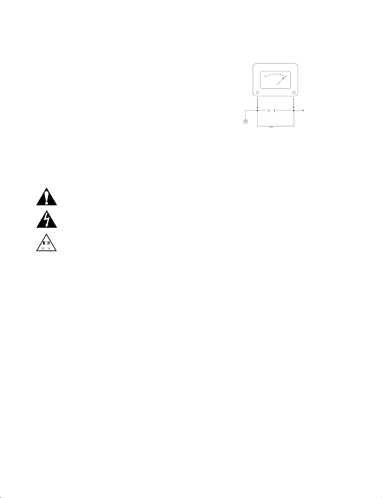
A.C. Voltmeter
Good Earth Ground
such as the Water
Pipe, Conduit, etc.
0.15uF
1500 OHM
10 WATT
Place this probe
on each exposed
metal part.
Page 5

1-4
SERVICING PRECAUTIONS
CAUTION: Before servicing the HOME THEATER COMBI
covered by this service data and its supplements and
addends, read and follow the
SAFETY PRECAUTIONS.
NOTE:
if unforeseen circumstances create conflict between
the following servicing precautions and any of the safety precautions in this publications, always follow the safety precautions.
Remember Safety First:
General Servicing Precautions
1. Always unplug the HOME THEATER COMBI AC power
cord from the AC power source before:
(1) Removing or reinstalling any component, circuit board,
module, or any other assembly.
(2) Disconnecting or reconnecting any internal electrical
plug or other electrical connection.
(3) Connecting a test substitute in parallel with an elec-
trolytic capacitor.
Caution: A wrong part substitution or incorrect
polarity installation of electrolytic capacitors may result
in an explosion hazard.
2. Do not spray chemicals on or near this HOME THEATER
COMBI or any of its assemblies.
3. Unless specified otherwise in this service data, clean
electrical contacts by applying an appropriate contact
cleaning solution to the contacts with a pipe cleaner,
cotton-tipped swab, or comparable soft applicator.
Unless specified otherwise in this service data, lubrication
of contacts is not required.
4. Do not defeat any plug/socket B+ voltage interlocks with
whitch instruments covered by this service manual might
be equipped.
5. Do not apply AC power to this HOME THEATER COMBI
and/or any of its electrical assemblies unless all solid-state
device heat sinks are correctly installed.
6. Always connect the test instrument ground lead to an
appropriate ground before connecting the test instrument
positive lead. Always remove the test instrument ground
lead last.
Insulation Checking Procedure
Disconnect the attachment plug from the AC outlet and turn
the power on. Connect an insulation resistance meter (500V)
to the blades of the attachment plug. The insulation resistance between each blade of the attachment plug and accessible conductive parts (Note 1) should be more than 1Mohm.
Note 1: Accessible Conductive Parts include Metal panels,
Input terminals, Earphone jacks,etc.
Electrostatically Sensitive (ES) Devices
Some semiconductor (solid state) devices can be damaged
easily by static electricity. Such components commonly are
called Electrostatically Sensitive (ES) Devices. Examples of
typical ES devices are integrated circuits and some field
effect transistors and semiconductor chip components.
The following techniques should be used to help reduce the
incidence of component damage caused by static electricity.
1. Immediately before handling any semiconductor component or semiconductor-equipped assembly, drain off any
electrostatic charge on your body by touching a known
earth ground. Alternatively, obtain and wear a commercially available discharging wrist strap device, which
should be removed for potential shock reasons prior to
applying power to the unit under test.
2. After removing an electrical assembly equipped with ES
devices, place the assembly on a conductive surface such
as aluminum foil, to prevent electrostatic charge buildup or
exposure of the assembly.
3. Use only a grounded-tip soldering iron to solder or unsolder
ES devices.
4. Use only an anti-static solder removal device. Some
solder removal devices not classified as “anti-static” can
generate electrical charges sufficient to damage ES
devices.
5. Do not use freon-propelled chemicals. These can
generate an electrical charge sufficient to damage ES
devices.
6. Do not remove a replacement ES device from its protective package until immediately before you are ready to
install it. (Most replacement ES devices are packaged with
leads electrically shorted together by conductive foam,
aluminum foil,or comparable conductive material).
7. Immediately before removing the protective material from
the leads of a replacement ES device, touch the protective
material to the chassis or circuit assembly into which the
device will be installed.
Caution: Be sure no power is applied to the chassis or
circuit, and observe all other safety precautions.
8. Minimize bodily motions when handling unpackaged
replacement ES devices. (Normally harmless motion such
as the brushing together of your clothes fabric or the lifting
of your foot from a carpeted floor can generate static electricity sufficient to damage an ES device.)
Page 6
1-5
SERVICE INFORMATION FOR EEPROM IC SETTING(VCR)
MODEL NAME HEX BINARY
LH-CX246 OPT1 38 00000000
OPT2 ED 00000000
OPT3 20 00000000
OPT4 8A 00000000
OPT5 41 00000000
OPT6 AF 00000000
LH-CX245 OPT1 38 00000000
OPT2 ED 00000000
OPT3 20 00000000
OPT4 8A 00000000
OPT5 41 00000000
OPT6 AF 00000000
LH-CX247 OPT1 38 00000000
OPT2 ED 00000000
OPT3 20 00000000
OPT4 8A 00000000
OPT5 41 00000000
OPT6 AF 00000000
LH-CX640 OPT1 38 00000000
OPT2 ED 00000000
OPT3 A0 00000000
OPT4 8A 00000000
OPT5 61 00000000
OPT6 AF 00000000
WR : OK I : EXIT MOVE :
F G
EDIT : DE
1. DETECT NEW EEPROM (OPTION EDIT
SCREEN)
- Eeprom EDIT screen automatically appears if
replacing Eeprom.
- Setup option data using the cursor Up/Down key
of a remote control.
(Setup upon BOM depending on OPT1~OPT6
model)
• Since an initial remote control is set to LG for LG
model, appropriately set optiona data using the
cursor Up/Down key.
2. EEPROM WRITED COMPLETE SCREEN
- Writes data on EEPROM by using REMOCON
"OK".
- If completing the option data screen with a menu
key, Powering Off is automatically done and the
option edit screen is arranged.
3. PG ADJUST
- Plays PAL SP TAPE for adjusting the AUTO PG.
- A 0:00:00 is played in the field if pressing the
front play with Remocon number "1" key played
during PAL SP.
- The 0:00:00 in the field represents position of the
TRACKING PRESET.
- "OFF" is displayed in the field if pressing the front
play key with the remocon number "1" in the status of the tracking preset pressed, and "ON" is
displayed in the field if AUTO PG operation is
automatically performed and completed.
- DECK STOP > plays if above operation is com-
pleted. Set operation is performed depending on
changed PG values. These values are stored in
the EEPROM area.
4. EEPROM INITIAL
- SETUP is displayed in the field if pressing the
FRONT REC KEY with the remocon number
"CLEAR" key pressed in the status of powering
Off.
- AUTO SEARCH is done since the initial screen
of ACMS is serviced if powering On.
- Check basic operation (PLAY/RECORD...)
EEPROM option code No. setting EEPROM option code No. setting procedure
NAME HEX BINARY
OPT1 00 00000000
OPT2 00 00000000
OPT3 00 00000000
OPT4 00 00000000
OPT5 00 00000000
OPT6 00 00000000
WR : OK I : EXIT MOVE : F G
EDIT : DE
MASKROM : R00
EEPROM : R00 LG CODE
Page 7
1-6
SERVICE INFORMATION FOR EEPROM (DVD)
* OPTION
• NTSC model doesn’t have VCR option and use DVD option B~F as VCR option. (only DVD exist)
• PAL model has another separate VCR option. (Both VCR and DVD exist)
MODEL
NAME
LH-CX245
LH-CX246
LH-CX247
LH-CX640
00 F7 87 05 FC 22 00 00 00 0A 00 00 00 00 00 00
00 F7 87 05 FC 22 00 00 00 0A 00 00 00 00 00 00
00 F7 87 05 FC 22 00 00 00 0A 00 00 00 00 00 00
00F78705FCA200000000000000000000
OPT OPT OPT OPT OPT OPT OPT OPT OPT OPT OPT OPT OPT OPT OPT OPT
123456789ABCDEFG
DETECT NEW EEPROM (OPTION EDIT SCREEN)
POWER ON
DVD LOGO Status (NO Disk status)
Remotecontrol
Pause key-->1-->4-->7-->2 in order.
Press number 0~9, Press charater
A~F (1~6 for a while)
Use arrow key (
F D G E
) to move
to approprite position and make
changes
Press pause key once
Change will be applied when power
OFF-->ON.
Page 8

1-7
SPECIFICATIONS
General
Power requirements Refer to main label
Power consumption Refer to main label
Dimensions (approx.) 430 X 81 X 360 mm (w/h/d)
Mass (approx.) 5.8 kg
Operating temperature 5˚C to 40˚C (41˚F to 95˚F)
Operating humidity 5 % to 90 %
Timer 24 hours display tape
DVD Section
Laser Semiconductor laser, wavelength 650 nm
Signal system PAL/NTSC
Frequency response DVD (PCM 96 kHz): 8 Hz to 44 kHz
DVD (PCM 48 kHz): 8 Hz to 20 kHz
CD: 8 Hz to 20 kHz
Signal-to-noise ratio More than 70 dB (analog out connectors only)
Harmonic distortion Less than 1.0%
Dynamic range More than 60 dB (DVD, CD)
Outputs
S-VIDEO OUT (Y) 1.0 V (p-p), 75 ohms, negative sync, Mini DIN 4-pin x 1
(C) 0.3 V (p-p) 75 ohms
VCR Section
Tape speed PAL/MESECAM; 23.39 mm/s (SP), 16.69 mm/s (LP)
NTSC (Playback only); 35.35 mm/s (SP), 16.67 mm/s (LP),
11.12 mm/s (EP)
Maximum recording time SP: 4 h (E-240 tape), LP: 8 h (E-240 tape)
Rewind time About 180 min (E-180 tape)
Input level VIDEO:1.0 V(p-p), 75 ohms, unbalanced
AUDIO: -6.0 dBm, more than 10 kohms (SCART)
-6.0 dBm, more than 47 kohms (RCA)
Output level VIDEO:1.0 V(p-p), 75 ohms, unbalanced
Signal-to-noise ratio VIDEO: More than 43 dB
AUDIO: More than 72 dB (Hi-Fi)
More than 42 dB (Mono)
Dynamic range AUDIO: More than 85 dB
Tuner Section
Tuning range FM: 87.5 - 108.0 MHz
AM: 522 - 1611 kHz
Intermediate frequency FM: 10.7 MHz
AM: 450 kHz
Amplifier(LH-CX245/LH-CX247)
Stereo mode 25W + 25W (6 ohm at 1 kHz, THD 10%)
Surround mode Front: 25W + 25W (THD 10%)
Centre: 25W
Surround: 25W + 25W (6 ohm at 1 kHz, THD 10%)
Subwoofer: 60W (8 ohm at 30 Hz, THD 10%)
Speaker Section(LH-CX245/LH-CX247)
Satellite Speaker (LHS-CX245T/LHS-CX247T) Passive Speaker (LHS-CX245W/LHS-CX247W)
Type 1 Way 1 Speaker 1 Way 1 Speaker
Impedance 8 Ω 8 Ω
Frequency Response 130 - 20,000 Hz 50 - 1,500 Hz
Sound Pressure Level 85 dB/W (1m) 82 dB/W (1m)
Rated Input Power 25W 60W
Max Input Power 50W 120W
Net Dimensions (W x H x D) 90 x 138.5 x 100 mm 160 x 350 x 345 mm
Net Weight 0.9 kg 4.5 kg
Page 9

1-8
Amplifier(LH-CX246)
Stereo mode 25W + 25W (6 ohm at 1 kHz, THD 10%)
Surround mode Front: 25W + 25W (THD 10%)
Centre: 25W
Surround: 25W + 25W (6 ohm at 1 kHz, THD 10%)
Subwoofer: 60W (8 ohm at 30 Hz, THD 10%)
Speaker Section(LH-CX246)
Satellite Speaker (LHS-CX246T) Passive Speaker (LHS-CX246W)
Type 1 Way 1 Speaker 1 Way 1 Speaker
Impedance 8 Ω 8 Ω
Frequency Response 130 - 20,000 Hz 50 - 1,500 Hz
Sound Pressure Level 85 dB/W (1m) 82 dB/W (1m)
Rated Input Power 25W 60W
Max Input Power 50W 120W
Net Dimensions (W x H x D) 89 x 130 x 114 mm 160 x 350 x 333 mm
Net Weight 0.54 kg 4.5 kg
Amplifier(LH-CX640)
Stereo mode 90W + 90W (6 ohm at 1 kHz, THD 10%)
Surround mode Front: 90W + 90W (THD 10%)
Centre: 90W
Surround: 90W + 90W (6 ohm at 1 kHz, THD 10%)
Subwoofer: 150W (4 ohm at 30 Hz, THD 10%)
Speaker Section(LH-CX640)
Satellite Speaker Centre speaker Passive Subwoofer
(LHS-CX640T) (LHS-CX640C) (LHS-CX640W)
Type 2 Way 2 Speaker 2 Way 2 Speaker 1 Way 1 Speaker
Impedance 6 Ω 6 Ω 4 Ω
Frequency Response 120 - 20,000 Hz 120 - 20,000 Hz 40 - 1,500 Hz
Sound Pressure Level 82 dB/W (1m) 82 dB/W (1m) 83 dB/W (1m)
Rated Input Power 90W 90W 150W
Max Input Power 180W 180W 300W
Net Dimensions (W x H x D) 104 x 233 x 120 mm 220 x 114 x 110 mm 195 x 380 x 419 mm
Net Weight 1.0 kg 1.0 kg 6.6 kg
• Design and specifications are subject to change without notice.
Manufactured under license from Dolby Laboratories. “Dolby” and the double-D symbol are trademarks of Dolby
Laboratories. Confidential unpublished works. Copyright 1992-1997 Dolby Laboratories. All rights reserved.
“DTS” and “DTS Digital Surround” are trademarks of Digital Theater Systems, Inc.
Page 10

2-1
SECTION 2
CABINET & MAIN CHASSIS
CONTENTS
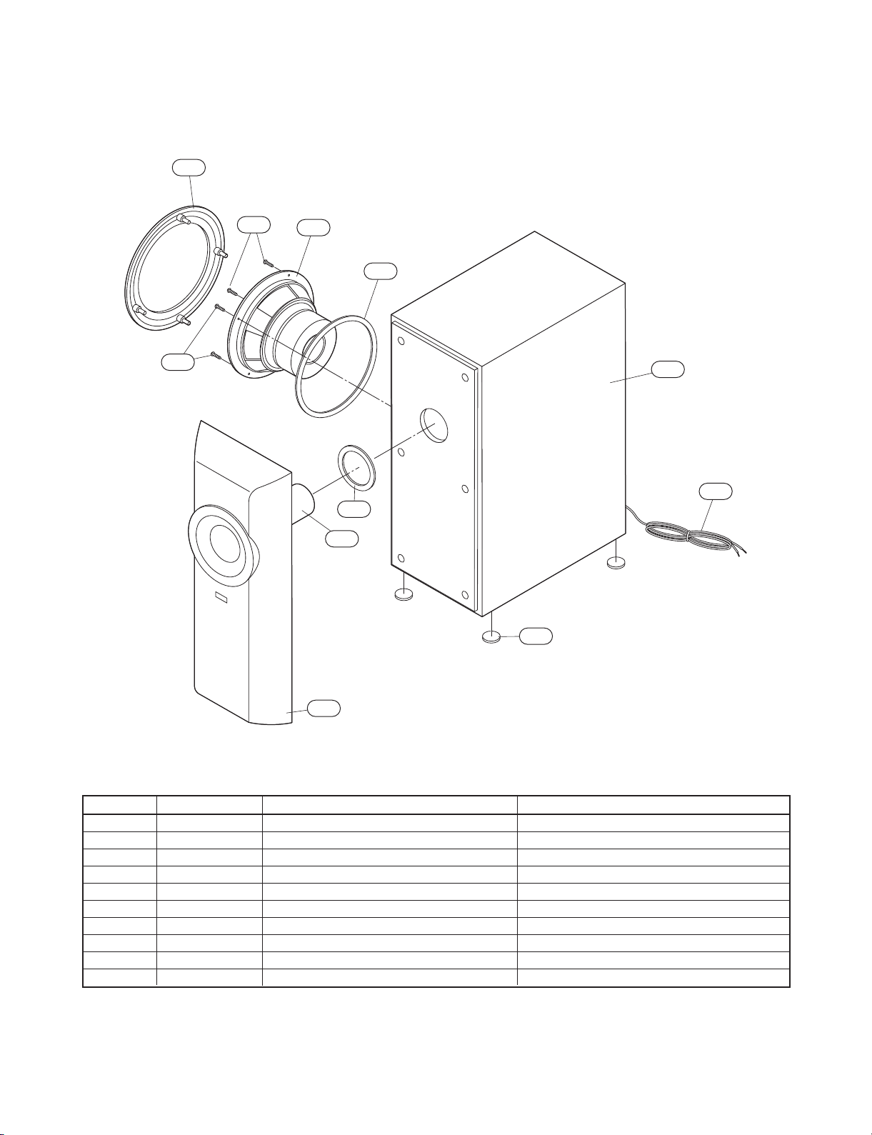
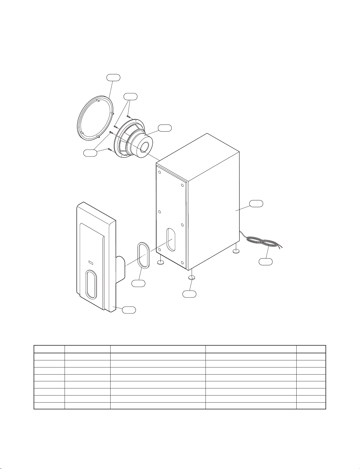
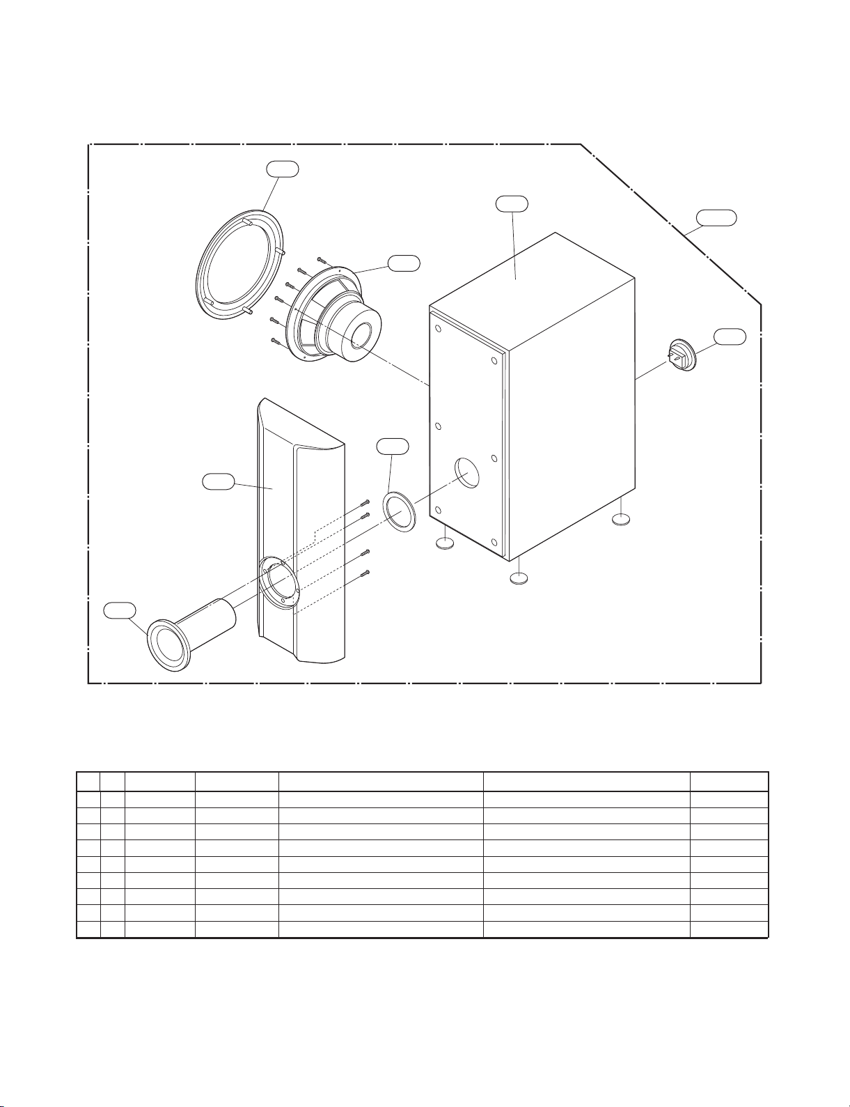
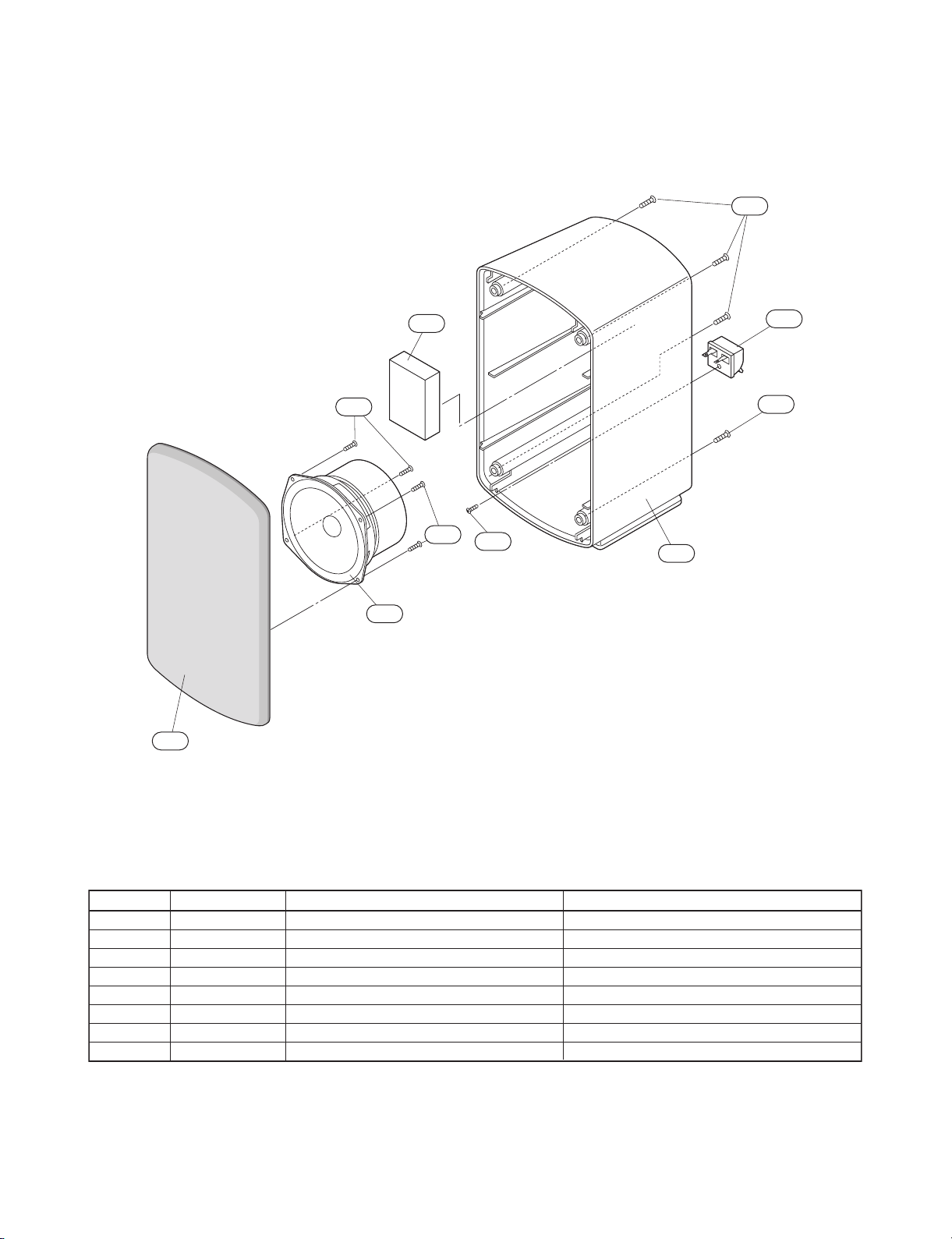
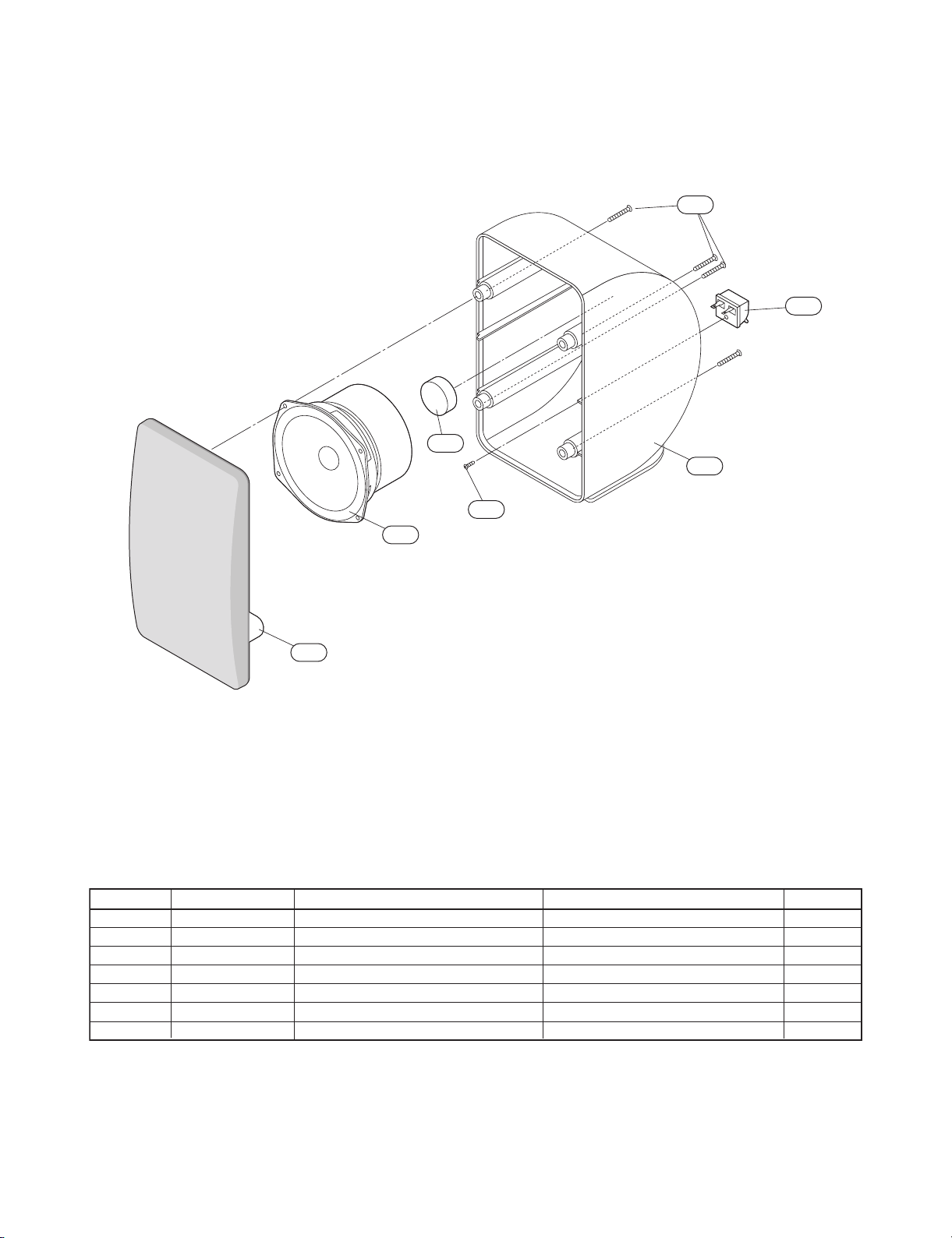
EXPLODED VIEWS .....................................................................................................................2-2
1. Cabinet and Main Frame Section ...........................................................................................2-2
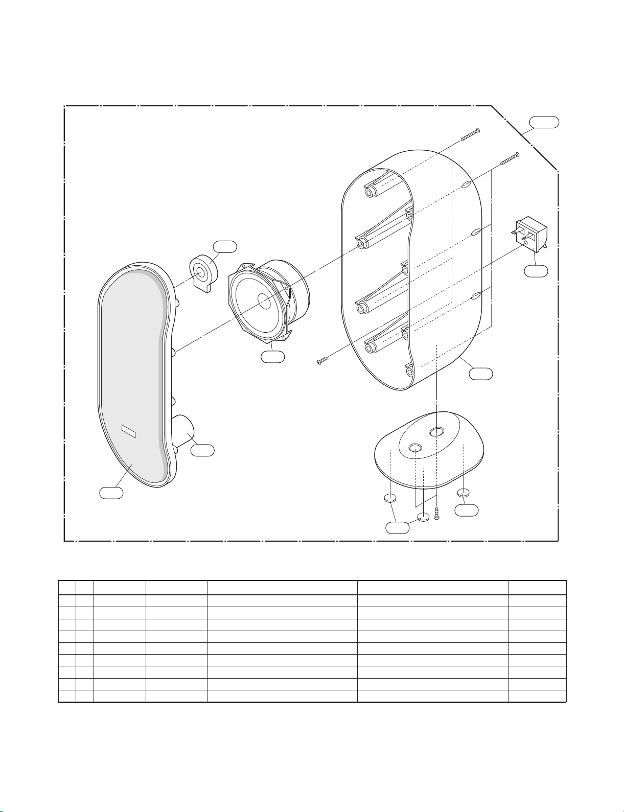
2. Woofer Speaker Section (LHS-CX245W/LHS-CX247W) .......................................................2-3
3. Woofer Speaker Section (LHS-CX246W) ..............................................................................2-4
4. Woofer Speaker Section (LHS-CX640W) ..............................................................................2-5
5. Setellite & Center Speaker Section (LHS-CX245T/LHS-CX247T) ........................................2-6
6. Setellite & Center Speaker Section (LHS-CX246T)...............................................................2-7
7. Setellite Speaker Section (LHS-CX640T)...............................................................................2-8
8. Center Speaker Section (LHS-CX640C).................................................................................2-9
9. Packing Accessory Section ..................................................................................................2-10
Page 11
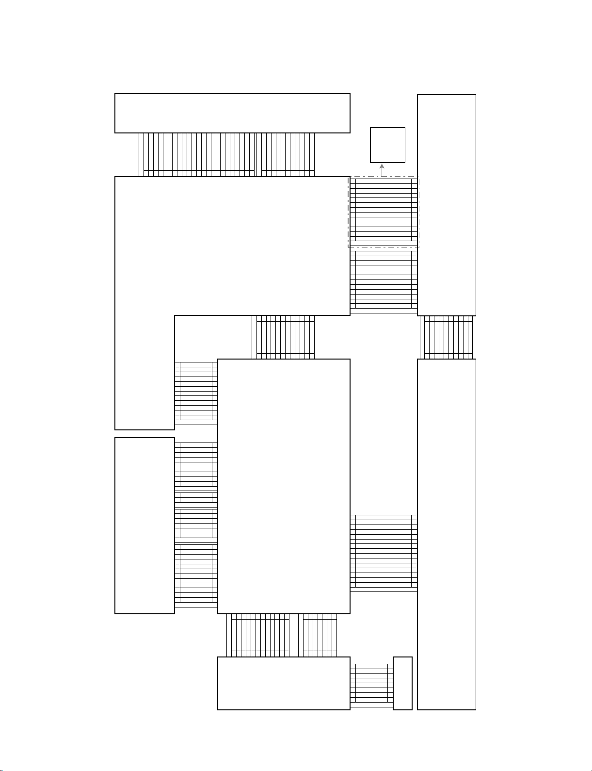
2-2
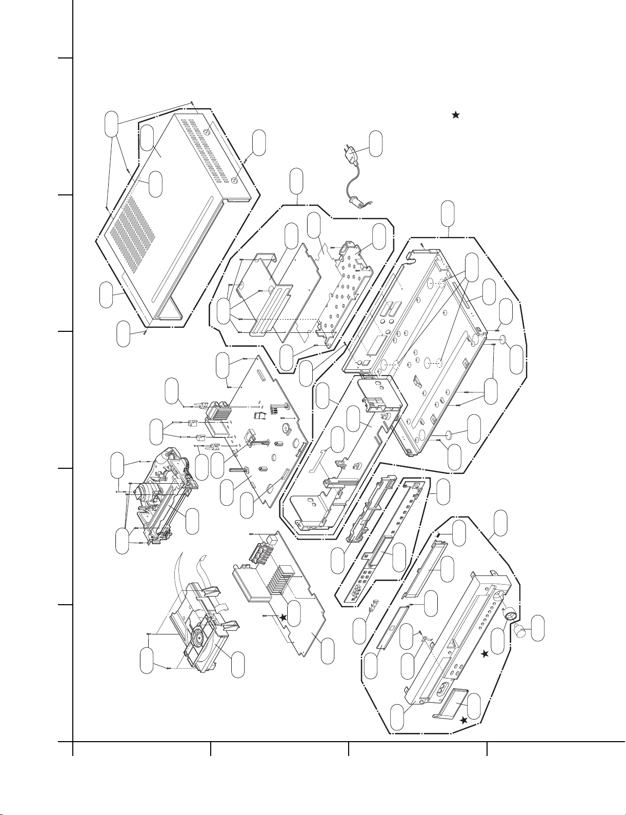
EXPLODED VIEWS
1. Cabinet and Main Frame Section
A
5
4
3
2
1
BCD
467
251
467
300
OPTIONAL PARTS
252
A47
264
A44
262
266
261A
250
468
467
471
470
469
469
323
470
453
462
260
1
26
262
452
330
452
261A
452
261A
A46
275
A00
457
457
A26
276
322
274
A41
285
276B
467
289
280
A50
A43
284
283
286
277
287
288
Page 12
2-3
LOCA. NO. PART NO. DESCRIPTION SPECIFICATION
951 3720RMF085A PANEL,FRONT SPK LHS-D6245W MOLD STANDARD
952 4766RM0097A FELT INSIDE 65 MM, OUTSIDE 85MM,THI
953 3091RMW099A CABINET ASSEMBLY SPK LHS-D6245W STANDARD FINE
954 5208RM0056A DUCT SPK LHS-D6245W OTHER PAPER PIP
955 6400WTTJ03A SPEAKER,WOOFER F65C-D365 TOPTONE WOOFER LHS-6
956 3701RM0104A NET ASSEMBLY SPK LHS-D6245W SP-8505
957 4766RM0005A FELT Audio WF,FE-3500SW,470X7X1T BL
959 353M050C SCREW,DRAWING BH 3.5X16 FBK
960 3610RM0046A FOOT SPK LHS-D6245W OTHER FOOT RUBB
961 6871RU9271F PWB(PCB) ASSEMBLY,SUBSET(AUDIO LHS-D6230W SUB WOOFER 2.5M, OR
2. Woofer Speaker Section (LHS-CX245W/LHS-CX247W)
956
959
959
955
957
958
961
952
954
952
951
Page 13
2-4
LOCA.NO. PART NO DESCRIPTION SPECIFICATION REMARKS
951 3720RMF081A PANEL,FRONT SPK LHS-D6240W MOLD FRONT PANE
952 4766RM0084A FELT 1T BLACK EVA
953 3091RMW094D CABINET ASSEMBLY SPK LHS-D6240W CABINET ASSY
955 6400WTTJ03A SPEAKER,WOOFER CW-165B40L SAMMI WOOFER LHS-D6
956 4766RM0005A FELT Audio WF,FE-3500SW,470X7X1T BL
959 353M050C SCREW,DRAWING BH 3.5X16 FBK
960 3610RM0024A FOOT SPK LMS-230/530 OTHER (EVA) PH
961 6871RU9271F PWB(PCB) ASSEMBLY,SUBSET(AUDIO LHS-D6230W SUB WOOFER 2.5M, OR
3. Woofer Speaker Section (LHS-CX246W)
956
959
955
959
953
961
952
960
951
Page 14
2-5
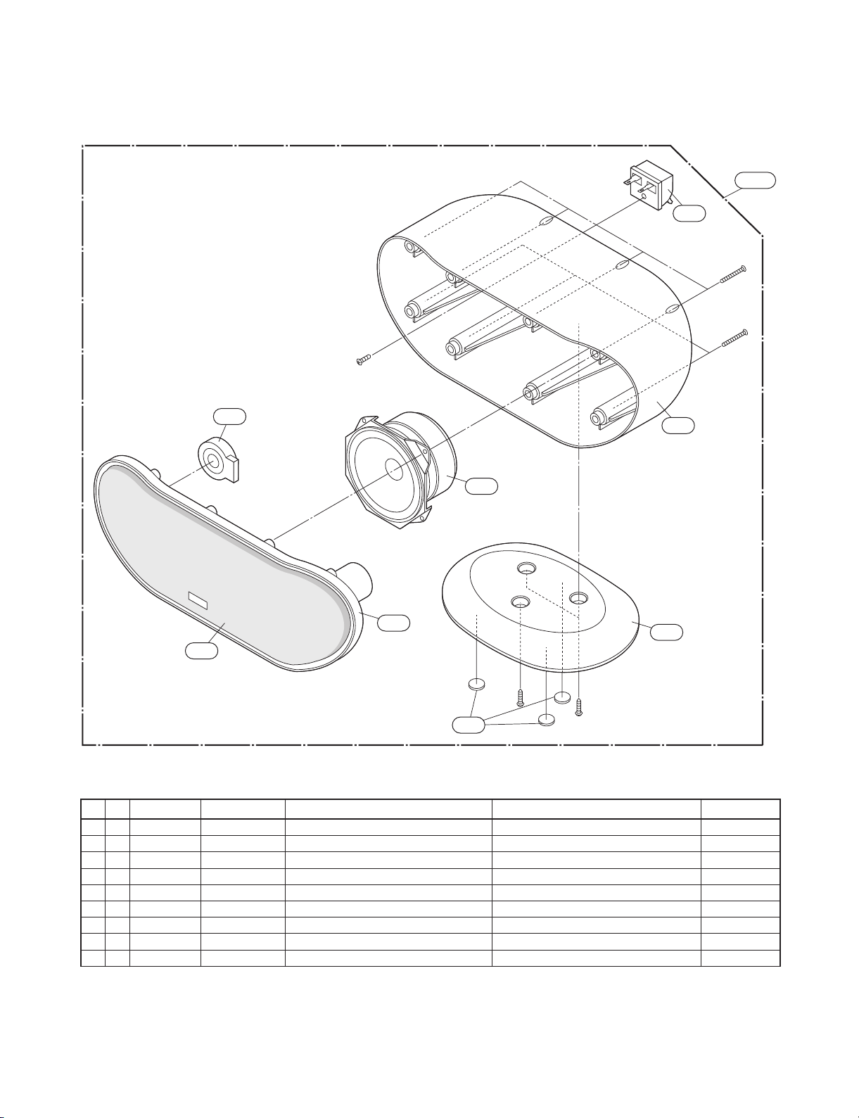
4. Woofer Speaker Section (LHS-CX640W)
952
953
955
951
954
A900
956
950
A900 6401RM0160A SPEAKER ASSEMBLY CW-210B150L-1 SAMMI LHS-C640W
950 5208RM0059A DUCT SPK LHS-T6540W MOLD CHROME PLA
951 3720RMM013A PANEL,AUDIO SPK LHS-T6540W MOLD FRONT (SIL
952 3701RM0110A NET ASSEMBLY SPK LHS-T6540W NET ASSY
953 6400WSMK03A SPEAKER,WOOFER CW-210B150L-1 SAMMI WOOFER 4 O
954 3091RMW107A CABINET ASSEMBLY SPK LHS-T6540W CABINET ASSY
955 4766RM0110A FELT 63*115*2T BLACK DUCT EV
956 6871RU9251A PWB(PCB) ASSEMBLY,SUBSET(AUDIO ASSY FE-5 000WE ROUND 2P TERMIN
957 3610RM0009A FOOT LXS-330, EVA(BLACK) PHI15X1T,
A
Page 15
2-6
5. Setellite & Center Speaker Section (LHS-CX245T/LHS-CX247T)
861
850
862
851
852
862
860
854
861
853
LOCA. NO. PART NO. DESCRIPTION SPECIFICATION
850 3701RM0103A NET ASSEMBLY SPK LHS-D6245T SP 8505
851 6400WTTC04A SPEAKER,FULLRANGE F30C-D366-2 TOPTONE W OOFER 6OH
852 4930RM0025A HOLDER AIR CO
853 3110RMP044A CASE LHS-D6245T MOLD STAND
854 6871RU4116B PWB(PCB) ASSEMBLY,SUBSET(AUDIO FE-3620TE 2P NEW TERMINAL 150M
860 353M025C SCREW,DRAWING TAPTITE, 3X10 FBK
861 353M025W SCREW,DRAWING + 2 D3.0 L14.0 MSWR3/FZB
862 353M025V SCREW,DRAWING + 2 D3.0 L6.0 MSWR3/FZB
VER LH-6230TE
ARD
Page 16
2-7
6. Setellite & Center Speaker Section (LHS-CX246T)
852
860
851
861
854
853
850
LOCA.NO. PART NO DESCRIPTION SPECIFICATION REMARKS
850 3701RM0093A NET ASSEMBLY SPK LHS-D6240T SP-8505
851 6400WTTC04A SPEAKER,WOOFER MSF-80SB20L-1 SAMMI WOOFER 6OH
852 4930RM0046A HOLDER
853 3110RMP042A CASE LHS-D6240T MOLD REAR CASE
854 6871RU4116B PWB(PCB) ASSEMBLY,SUBSET(AUDIO FE-3620TE 2P NEW
860 353M025G SCREW,DRAWING TAPTITE, 3X10 FZMY
861 353M025H SCREW,DRAWING TAPTITE, 3X16 FZMY
SPK LHS-D6240T MOLD PREVENTION
TERMINAL 150M
Page 17
2-8
7. Setellite Speaker Section (LHS-CX640T)
852
853
A800
855
854
851
850
856
857
A800 6401RM0158A SPEAKER ASSEMBLY MSF-90SB90L SAMMI LHS-C640T SV
850 3530RMP044A GRILLE LHS-E6740T PRESS BK 0.6T
851 3720RMM015A PANEL,AUDIO SPK LHS-E6740T/C MOLD FRONT
852 6400DSMX02A SPEAKER,TWEETER DT-11ND-1 SAMMI TWEETER(DOME)
853 6400WSMC05A SPEAKER,WOOFER MSF-90SB90L SAMMI WOOFER 6 OHM
854 3110RMP073A CASE LHS-E6740T MOLD REAR
855 6871RU0038A PWB(PCB) ASSEMBLY,SUBSET(AUDIO LHS-C640/T6745/E740 STANDARD 2
856 3040RMP037A BASE LHS-E6740T MOLD BOTTOM STAND
857 3610RM0044A FOOT SPK LHS-T6540T/C OTHER EVA PHI
Page 18
2-9
8. Center Speaker Section (LHS-CX640C)
A700
755
750
752
751
754
753
756
756
A700 6401RM0159A SPEAKER ASSEMBLY MSF-90SB90L SAMMI LHS-C640C SV
750 3530RMP044B GRILLE LHS-E6740C PRESS BK 0.6T
751 3720RMM015A PANEL,AUDIO SPK LHS-E6740T/C MOLD FRONT
752 6400DSMX02A SPEAKER,TWEETER DT-11ND-1 SAMMI TWEETER(DOME)
753 6400WSMC05A SPEAKER,WOOFER MSF-90SB90L SAMMI WOOFER 6 OHM
754 3110RMP072A CASE LHS-E6740C MOLD REAR
755 6871RU0038A PWB(PCB) ASSEMBLY,SUBSET(AUDIO LHS-C640/T6745/E740 STANDARD 2
756 3040RMP036A BASE LHS-E6740C MOLD BOTTOM STAND
757 3610RM0044A FOOT SPK LHS-T6540T/C OTHER EVA PHI
Page 19
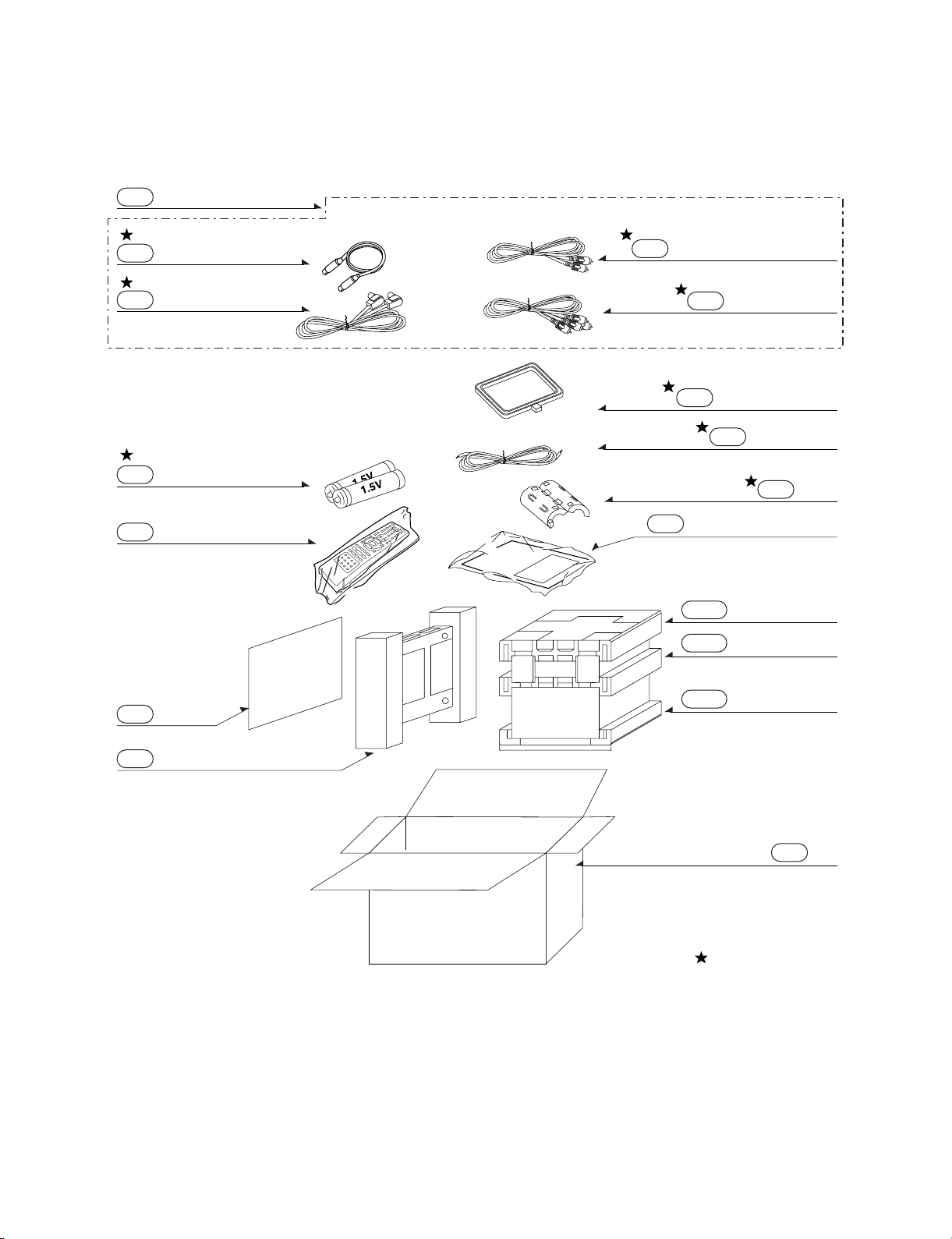
2-10
BATTERY
CABLE, COAXIAL
CABLE SET ASS’Y, RF
OPTIONAL PARTS
INSTRUCTION ASSEMBLY
BOX
REMOCON
BAG
PACKING
PLUG ASS’Y 1WAY(YELLOW)
ANTENNA LOOP(AM)
ANTENNA (FM)
PLUG ASS’Y 2WAY
PACKING, CASING
PACKING, CASING
PACKING, CASING
810
811
812
824
825
826
801
802
806
CABLE, COAXIAL
822
808
900
804
803
803A
803B
803C
FILTER
9. Packing Accessory Section
Page 20

3-1
SECTION 3
ELECTRICAL
CONTENTS
OVERALL WIRING DIAGRAM .............................3-2
VCR PART
ELECTRICAL ADJUSTMENT
PROCEDURES
...........................................................3-3
ELECTRICAL TROUBLESHOOTING
GUIDE
............................................................................3-4
1. POWER(SMPS) CIRCUIT.......................................3-4
2. SYSTEM/KEY CIRCUIT..........................................3-6
3. SERVO CIRCUIT ....................................................3-7
4. Y/C CIRCUIT.........................................................3-10
5. Hi-Fi CIRCUIT.......................................................3-14
6. TUNER/IF CIRCUIT ..............................................3-17
BLOCK DIAGRAMS ...............................................3-19
1. POWER(SMPS) BLOCK DIAGRAM 1 .................3-19
2. POWER(SMPS) BLOCK DIAGRAM 2 .................3-21
3. TU/IF, NICAM & A2 BLOCK DIAGRAM ..............3-23
4. VPS BLOCK DIAGRAM .......................................3-24
5. Y/C BLOCK DIAGRAM ........................................3-25
6. Hi-Fi BLOCK DIAGRAM ......................................3-27
7. SYSTEM BLOCK DIAGRAM ...............................3-29
CIRCUIT DIAGRAMS .............................................3-31
1. POWER(SMPS) CIRCUIT DIAGRAM 1_200W....3-31
2. POWER(SMPS) CIRCUIT DIAGRAM 1_400W....3-33
3. POWER(SMPS) CIRCUIT DIAGRAM 2 ...............3-35
4. TU/IF, NICAM & A2 CIRCUIT DIAGRAM.............3-37
5. A/V CIRCUIT DIAGRAM.......................................3-39
6. HI-FI CIRCUIT DIAGRAM ....................................3-41
7. SCART(JACK) CIRCUIT DIAGRAM....................3-43
8. SYSTEM CIRCUIT DIAGRAM..............................3-45
9. TIMER CIRCUIT DIAGRAM_0TOOL ...................3-47
10. TIMER CIRCUIT DIAGRAM_5TOOL / 7TOOL ..3-49
11. TIMER CIRCUIT DIAGRAM_6TOOL..................3-51
• WAVEFORM & VOLTAGE SHEET ........................3-53
• CIRCUIT VOLTAGE CHART ..................................3-55
PRINTED CIRCUIT DIAGRAMS ........................3-59
1. MAIN P.C.BOARD ................................................3-59
2. KEY(LEFT) P.C.BOARD ......................................3-61
3. KEY(RIGHT) P.C.BOARD.....................................3-63
4. SMPS P.C.BOARD ..............................................3-65
DVD PART
ELECTRICAL TROUBLESHOOTING
GUIDE
..........................................................................3-67
1. SYSTEM OPERATION FLOW..............................3-67
2. SYSTEM TEST FLOW..........................................3-68
DETAILS AND WAVEFORMS ON SYSTEM
TEST AND DEBUGGING......................................3-74
1. SYSTEM 27MHZ CLOCK, RESET,
FLASH R/W SIGNAL............................................3-74
2. SDRAM CLOCK ...................................................3-76
3. TRAY OPEN/CLOSE SIGNAL..............................3-76
4. SLED CONTROL RELATED SIGNAL
(NO DISC CONDITION)........................................3-77
5. LENS CONTROL RELATED SIGNAL
(NO DISC CONDITION)........................................3-77
6. LASER POWER CONTROL RELATED
SIGNAL(NO DISC CONDITION) ..........................3-78
7. DISC TYPE JUDGEMENT WAVEFORM..............3-78
8. FOCUS ON WAVEFORM .....................................3-80
9. SPINDLE CONTROL WAVEFORM
(NO DISC CONDITION)........................................3-81
10. TRACKING CONTROL RELATED
SIGNAL(SYSTEM CHECKING) .........................3-82
11. MT1389 AUDIO OPTICAL AND COAXIAL
OUTPUT(SPDIF).................................................3-83
12. MT1389 VIDEO OUTPUT WAVEFORM .............3-83
13. MT1389 AUDIO OUTPUT TO AUDIO DAC .......3-84
14. AUDIO OUTPUT FROM AUDIO DAC ................3-85
15. DVD & AMP WAVEFORMS................................3-86
BLOCK DIAGRAMS ...............................................3-87
1. OVERALL BLOCK DIAGRAM_200W ..................3-87
2. OVERALL BLOCK DIAGRAM_400W ..................3-88
3. SERVO BLOCK DIAGRAM ..................................3-89
4. MPEG & MEMORY BLOCK DIAGRAM...............3-90
5. VIDEO & AUDIO BLOCK DIAGRAM...................3-91
6. DVD & AMP BLOCK DIAGRAM ..........................3-92
CIRCUIT DIAGRAMS .............................................3-93
1. MPEG CIRCUIT DIAGRAM..................................3-93
2. RF & SERVO CIRCUIT DIAGRAM ......................3-95
3. AUDIO, µ_COM
CIRCUIT DIAGRAM(DVD & AMP) .......................3-97
4. DIGITAL AMP CIRCUIT DIAGRAM
(DVD & AMP)_200W ............................................3-99
5. DIGITAL AMP CIRCUIT DIAGRAM
(DVD & AMP)_400W ..........................................3-101
6. PWM & CODEIC CIRCUIT DIAGRAM
(DVD & AMP)_200W ..........................................3-103
7. PWM & CODEIC CIRCUIT DIAGRAM
(DVD & AMP)_400W ..........................................3-105
8. INTERFACE CIRCUIT DIAGRAM
(DVD & AMP)_200W ..........................................3-107
9. INTERFACE CIRCUIT DIAGRAM
(DVD & AMP)_400W ..........................................3-109
• CIRCUIT VOLTAGE CHART_200W .....................3-111
• CIRCUIT VOLTAGE CHART_200W.....................3-115
PRINTED CIRCUIT DIAGRAMS.......................3-119
1. DVD & AMP P.C.BOARD_200W ........................3-119
2. DVD & AMP P.C.BOARD_400W........................3-121
Page 21
3-2
OVERALL WIRING DIAGRAM
123456789
101112
KEY RTN 0
KEY RTN 1
5.3VA
VIDEO IN
GND
AUDIO "L" IN
GND
AUDIO "R" IN
GND
FD(-)
-29VA
FD(+)
123456789
101112
P6M01 PM601
123456789
101112
DVD VIDEO
A.GND
DVD A, 'L'
A.GND
DVD A, 'R'
A.GND
AUDIO 'L'
AUDIO 'R'
A.GND
DVD B
DVD G
DVD R
123456789
101112
PMD02 PDM02
123456789
10111213141516171819202122
23
VCC(HF)
RF
DVD-LD
DVD-PD
VOL(DVD)
GND
VC-INPUT
VCC
F
E
A
D
C
B
F(+)
T(-)
T(+)
F(-)
PICK-SEL
GND
CD-LD
CD-PD
VOL(CD)
123456789
10111213141516171819202122
23
PMD02
123456789
10
11
SPM+
SPM-
FM(+)
FM(-)
LM(-)
LM(+)
SW(OPEN)
SW(CLOSE)
GND
SW(LEAD IN)
GND
123456789
10
11
PMD03
123456789
10
32VA
32VA
GND
GND
5VA
GNDNCGND
NC
PWR SENSE
123456789
10
PSW01 PN901
1
2
3
4
5
6
7
8
9
10
11
12
CFG
12VA(CAP)
5.2VA
CAP REV 'H'
I-LIMIT
MOTOR GND
GND
12VA(DRUM)
CAP CTL
L/M CTL
DFG/PG
DRUM CTL
1
2
3
4
5
6
7
8
9
10
11
12
PMC01
1
2
3
4
5
6
7
8
9
SP A PB
SP REC
SP B PB
LP R PB
LP REC
LP A PB
Hi-Fi A PB
Hi-Fi REC
Hi-Fi B PB
1
2
3
4
5
6
7
8
9
P3D01
1
2
3
4
5
6
7
8
GND
KEY RTN 1
GND
F.A.R.IN
GND
F.A.L.IN
GND
VIDEO IN
1
2
3
4
5
6
7
8
P6603 P6602
1
2
3
4
5
6
7
8
9
10
11
12
GND
SPDIF
GND
5.2VA
AMP-CLK
AMP-ENA
M-RESET
AMP-DATA 0
AMP DATA 1
A-MUTE
GND
OPTICAL IN
1
2
3
4
5
6
7
8
9
10
11
12
CN901 PVD04
1
2
3
4
5
6
7
8
9
10
11
12
13
TUNED
STEREO
12VA
L-OUT
AGND
R-OUT
PLL-CE
PLL-DI
PLL-CLK
PLL-D0
DGND
RDS-CLK
RDS-DATA
1
2
3
4
5
6
7
8
9
10
11
12
13
PN101 PVD04
1
2
3
4
5
6
7
8
9
10
11
12
13
14
15
GND
GND
5.3VA
5.3VA
GND
3.8VA
3.8VA
GND
13VA
GND
33VA
GND
-29VA
FD(-)
FD(+)
1
2
3
4
5
6
7
8
9
10
11
12
13
14
15
PSV01 PVS01
1
2
3
4
5
6
7
8
9
10
11
12
DVD ENA(M-REC)
A.GND
DVD DATA OUT(RXDO)
DVD DATA IN(TXDO)
DVD CLK(SCKO)
DVD RESET(M-RESET)
AMP DATA IN
AMP CLK
GND
AMP ENA
AMP DATA OUT
A-MUTE 'H'
1
2
3
4
5
6
7
8
9
10
11
12
PMD01 PDM01
1
2
3
4
5
6
CTL(+)
CTL(-)
A/E(+)
A/E(-)
A.REC
A.PB
1
2
3
4
5
6
P3D02
12GND
FULL ERASE
1
2
P3D03
1234567
REMOCON
GND
FLD CLK
FLD DATA
FLD ENV
VOLUMN DOWN
VOLUMN UP
1234567
P6M02 PM602
VCR
DECK
VCR MAIN
KEY BOARD
TIMER
BOARD
SMPS BOARD AMP BOARD
MD
AM/FM
TUNER
OPTION
MPEG BOARD
Page 22
3-3
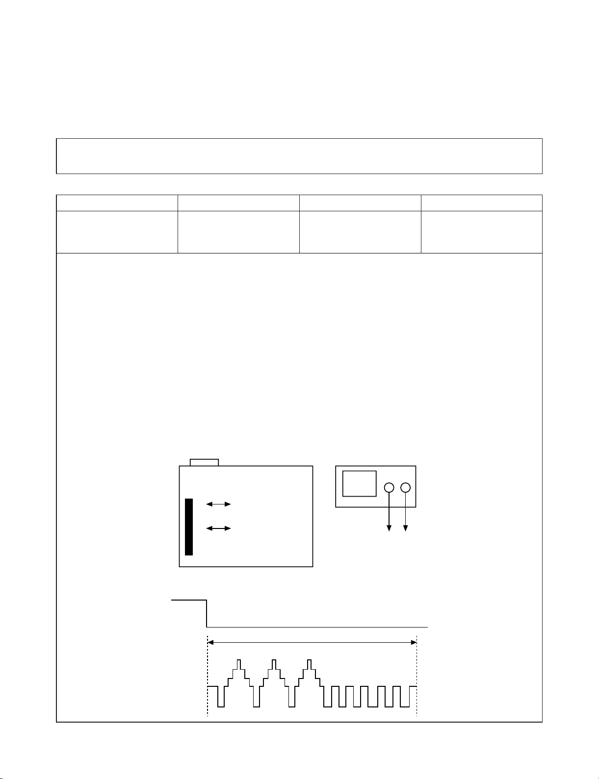
ELECTRICAL ADJUSTMENT PROCEDURES
1. Servo Adjustment
1) PG Adjustment
• Test Equipment
• Adjustment And Specification
a) OSCILLOSCOPE b) PAL MODEL : PAL SP TEST TAPE
MODE
PLAY
• Adjustment Procedure
a) Insert the SP Test Tape and play.
Note - Adjust the distance of X, pressing the Tracking(+) or Tracking(-) when the “ATR” is blink after the
SP Test Tape is inserted.
b) Connect the CH1 of the oscilloscope to the H/SW(W373, W374) and CH2 to the Video Out for the VCR.
c) Trigger the mixed Combo Video Signal of CH2 to the CH1 H/SW(W373, W374), and then check the dis-
tance (time difference), which is from the selected A(B) Head point of the H/SW(W373, W374) signal to
the starting point of the vertical synchronized signal, to 6.5H ± 0.5H (416µs, 1H=64µs).
• PG Adjustment Method
a-1) Payback the SP standard tape
b-2) Press the “OK” key on the Remote controller and the “REC” key on the Front Panel the same time,
then it goes in to Tracking initial mode.
c-3) Repeat the above step(No.b-2), then it finishes the PG adjusting automatically.
d-4) Stop the playback, then it goes out to PG adjusting mode after mony the PG data.
• CONNECTION
• WAVEFORM
V.Out
H/SW(W373, W374)
6.5 ± 0.5H
MEASUREMENT POINT ADJUSTMENT POINT SPECIFICATION
V.Out
H/SW
W373
W374
OSCILLOSCOPE
CH1CH2
V.out
H/SW
(W373, W374)
H/SW
Composite
VIDEO
6.5H(416us)
VCR PART
Page 23
3-4
ELECTRICAL TROUBLESHOOTING GUIDE
1. Power(SMPS) CIRCUIT
NO 5.3VA.
Replace the F101.
(Use the same Fuse)
Is the F101 normal?
Is the TH101
normal?
Is the BD101
normal?
NO
NO
NO
NO
NO
NO
NO
NO
NO
NO
Replace the
BD101.
Replace the TH101.
Is the D105
normal?
Check or Replace
the D105.
Replace the D129.
Replace the IC106.
Replace the D127.
Replace the D126.
Replace the D125.
Replace the D124.
YES
YES
YES
YES
YES
YES
YES
YES
YES
YES
YES
Is Vcc(12~28V) supplied to IC104 Pin3?
Is the D129 nor-
mal?
Is there about 2.5V
at the IC106 Vref?
Is the D127
normal?
Is the D126
normal?
Is the D125
normal?
Is the D124
normal?
Check the Main PCB
Power supply Line short?
(1) No 5.3VA (SYS/Hi-Fi/TUNER)
NO 5.0VA.
Check or Replace
the D129.
Is there about 5.3V
at the Q168 Emitter?
Does the “H” signal
appear at the Q162?
Check or Replace
the Q162.
NO
Check the µ-com
PWRCTL ‘H’
NO
YES
YES
YES
(2) No 5.0VA
NO 3.3VA.
Check or Replace
the D127.
Is there about 3.8V
at the IC162 Pin1?
Check or Replace
the IC162.
NO
YES
YES
(3) No 3.3VA
NO 12VA.
Check or Replace
the D126.
Is there about 13V
at the Q161 C?
Check or Replace
the Q161.
NO
YES
YES
(4) No 12VA
NO
NO
NO
NO
NO
Page 24
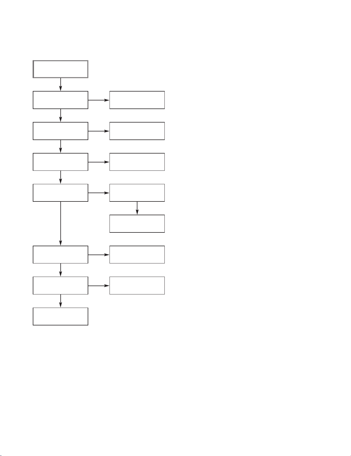
3-5
NO 32VA.
Replace the F101.
(use the same Fuse)
Is the F101 normal?
Is the TH101
normal?
Is the BD101
normal?
NO
NO
NO
Replace the BD101.
Replace the TH101.
NO
NO
NO
Is the D108
normal?
Check or Replace
the D108.
Replace the D122.
Replace the IC103.
YES
YES
YES
YES
YES
YES
YES
Is Vcc(12~23V) supplied to IC101 Pin3?
Is the D122
normal?
Is there about 2.5V
at the IC103?
Check the Woofer Main PCB
Power supply Line short or not?
(5) No 32VA
YES
Page 25
3-6
2. SYSTEM/KEY CIRCUIT
(1) AUTO STOP
(2) The unstable loading of a Cassette tape
Auto Stop
Does the SW25 waveform
appear at the IC501
Pin105?
Do the T-UP Reel Pulses
appear at the IC501 Pin49?
Is 12V applied to the
PMC01 Pin8?
Check the Drum Motor
signal.
Does 5.2V appear at the
RS501?
Check the Power Circuit.
Check the Power.
Is 5.3V applied to the
R544 ?
Refer to SMPS 5.3VA
troubleshooting.
Check the IC501
Pins68, 69, 70, 71.
Do T/UP Reel Pulses
appear at the Q514
Base terminal ?
Replace the T/UP Reel
Sensor (RS501).
Check the CST SW and
the peripheral circuitry.
Replace the IC501.
The unstable loading of a
Cassette tape
Does the “H” signal appear
at the IC501 Pin30 during
inserting the CST ?
Does the “L” signal appear
at the IC501 Pin72 during
inserting the CST?
Check the Deck
Mechanism.
Caution :
Auto stop can occur because Grease or Oil is dried up
YES
YES
YES
NO
YES
YES
YES
YES
NO
NO
NO
NO
NO
NO NO
YES
YES YES
Page 26
3-7
3. SERVO CIRCUIT
(1) Unstable Video in PB MODE
Unstable Video in
PB Mode.
Does the Noise level of the
screen change
periodically?
Do the CTL pulses appear
at the IC501 Pin8?
Is adjusting the height of
the CTL Head accurate?
Readjust the height of the
CTL Head.
Replace the IC501.
Refer to “When the Y signal
doesn’t appear on the
screen in PB Mode”.
Does the CFG waveform
appear at the IC501
Pin9?
On tracking do the CTL
pulses move?
Does the Video Envelope
waveform appear at the
IC501 Pin24?
Replace the IC501.
YES
YES
YES
YES
YES
YES
NO
NO
NO
NO
(2) When the Drum Motor
(2) doesn’t run.
Do the DFG Pulses appear
at the PMC01 Pin11?
Replace the Cap M.
Aren’t the foil patterns and
the Components between
IC501 Pin104 and PMC01
Pin11 short?
Replace the IC501.
Refer to “(2)
No 12VA of Power section”
Do the Drum PWM Pulses
appear at the IC501
Pin107?
Aren’t the foil patterns and
the Components between
IC501 Pin107 and PMC01
Pin12 short?
Do the DFG Pulses appear
at the IC501 Pin104?
Do the Drum PWM Pulses
appear at the IC501
Pin107?
Aren’t the connecting patterns and the Components
between IC501 Pin107 and PMC01 Pin12 short?
When the Drum Motor
doesn’t run,
Does 12V appear at the
PMC01 Pin8?
Does 2.8V appear at the
PMC01 Pin12?
Check the connector
(PMC01) and the Drum
Motor Ass’y.
NO
YES
YES
YES
NO
NO
NO
NO
NO
YES
YES
YES
Page 27
3-8
Does the CFG signal appear at the
PMC01 Pin1?
Does the PWM signal appear at the
IC501 Pin108?
Does 2.8V appear at the PMC01?
Check the PMC01 and the Capstan
Motor Ass’y.
Does the Capstan PWM signal appear at
the IC501 Pin108?
Aren’t the foil patterns and Components
between IC501 Pin108 and PMC01
Pin9 short?
Does the CFG signal come into the
IC501 Pin9?
Aren’t the foil patterns and Components
between IC501 Pin108 and PMC01
Pin9 short?
2. SERVO CIRCUIT
(3) When the Capstan Motor doesn’t run,
NO
NO
NO
YES
YES
YES
When the Capstan Motor doesn’t run,
Does 12VA appear at the PMC01?
YES
Replace the IC501.
YES
NO
NO
YES
Refer to “SMPS(CAPSTAN/12Volt)
Trouble Shooting”.
Aren’t the foil patterns and component
between IC501 Pin9 and PMC01
Pin1 short?
Check the Capstan Motor Ass’y.
NO
Page 28
3-9
2. SERVO CIRCUIT
(4) KEY doesn’t working
KEY doesn’t working.
Is 5V applied to the IC501
Pin36?
Does LED or FLD change
when a function button is
pressed?
Refer to “SMPS 5.3VA
Trouble Shooting”.
Replace the defective
switches.
YES
NO
NO
Page 29
3-10
4. Y/C CIRCUIT
(1) No Video in EE Mode,
No Video in EE Mode
Check the 24Pin of Tuner.
Does the Video signal
appear at the IC301 Pin48?
Is 5V applied to the IC301
Pins18, 24, 42, 55, 72, 91?
Does the Video signal
appear at the IC301 Pin65?
Does the Video signal
appear at the IC501 Pin19?
Does the Video signal
appear at the Emitter terminal of the Q307, Q308?
Check the 5.2VT, 5.3VA
Line. (Power Circuit)
Is I2C BUS signal applied to
the IC301 Pins68, 69?
Check C316. (AGC)
Chck the path of the signal
between the IC301 Pin65
and IC501 Pin17.
Replace the IC301.
Does the 12VT, 5.3VA
appear at the Emitter terminal of the Q804, Q308.
Replace the Q804, Q308.
Check the 12VT, 5.3VA
Line. (Power Circuit)
Check the System Circuit.
(Refer to ‘SYSTEM I2C BUS
CHECK Trouble Shooting’)
YES
YES
YES
YES
YES
YES
YES
NO
NO
NO
NO
NO
NO
NO
Page 30

3-11
3. Y/C CIRCUIT
(2) When the Y(Luminance) signal doesn’t appear on the screen in PB Mode,
Is 5.2VT, 5.3VA applied to the
IC301 Pins24, 42, 55, 72, 91?
Is the I2C Bus siganl applied
to the IC301 Pins68, 69 ?
Does the normal RF signal
appear at the IC301 Pin78?
Check the line of the 5.2VT,
5.3VA Line. (Power Circuit)
Check the System Circuit.
(IC501 Pin105)
Check the V.H.S/W level.
(Check R303, R304)
Replace the IC301.
Refer to ‘SYSTEM I2C BUS
CHECK Trouble Shooting’.
Is the V.H.S/W signal
applied to the IC301 Pin70?
Is V.H.S/W “H” about 3.4V
at the IC301 Pin70?
Clean the Drum.
Check the path of the
Y(Luminance) RF signal.
(Check C327)
Check the path of the
Y(Luminance) RF signal.
(Check the C312)
Does the Y(Luminance) RF
signal appear at the IC301
Pin76?
Is the Y(Luminance) Video
waveform showed up at
theIC301 Pin43?
Replace the IC301.
NO
NO
NO
NO
NO
NO
NO
NO
YES
YES
YES
YES
YES
YES
YES
YES
YES
Page 31

3-12
3. Y/C CIRCUIT
(3) When the C(Color) signal doesn’t appear on the screen in PB Mode,
Is 5.2VT/5.3VA applied to the
IC301 Pins24, 42, 55, 72, 91.
Is the Color Rotary signal
applied to the IC301
Pin70?
Check the line of the 5.2VT/
5.3VA Line. (Power Circuit)
Replace the X301.
Check the Color Pass.
Check the Color Rotary
Circuit. (IC501 Pin99 )
Check the Color Rotary
level. (Check the R303)
Does the X301(4.43MHZ)
oscillate?
Replace the IC301.
Does the Color signal
appear at the IC301 Pin21?
Is Color Rotary “H”
about 3.4V?
Replace the IC301.
NO
NO
NO
YES
YES
YES
YES
NO
NO
NO
YES
Does the Color signal
appear at the IC301
Pin25 ?
Page 32

3-13
3. Y/C CIRCUIT
(4) When the Video signal doesn’t appear on the screen in REC Mode,
Is the EE signal normal?
Is 5.2VT/5.3VA applied to the
IC301 Pins24,42,55,72,91?
Does the RF signal appear
at the IC301 Pin78?
Check EE Mode.
Check the System of REC
‘H’. (the IC501 Pin47
/ the D301)
Replace the IC301.
Check the line of the 5.2VT/
5.3VA Line.(Power Circuit)
Check PB Mode.
Is the REC ‘H’ signal
(about 4V) applied to the
IC301 Pin80?
Check the circuit of the
IC301 Pins85, 86.
Check REC Luminance
Pass & Color Pass.
Does PB Mdoe operate
normally?
Does the REC RF signal
appear at the IC301
Pins88,89,94,95?
Check the Drum &
Drum Connector
YES
YES
YES
YES
YES
NO
NO
NO
NO
NO
NO
YES
YES
YES
Page 33

3-14
5. Hi-Fi CIRCUIT
(A) No Sound(EE Mode)
YES
No Sound.
Check the TU Audio of IC801
Pins1, 3.
Check the DVD Audio of IC801
Pins4, 5.
Check the AV1 Audio of IC801
Pins6, 7.
Check the AV2 Audio of IC801
Pins8, 9.
Check the AV3 Audio of IC801
Pins10, 11.
Check the Vcc of IC801 Pins34, 40,
IC802 Pin4.
YES
Check the IIC Clock and DATA at
IC801 Pins42, 43, IC802 Pins32, 33.
YES
Check the Audio of IC801 Pins16, 17.
YES
Check the Audio of IC802 Pins22, 26.
YES
Check the JK801.
Check the IC751 Pins30, 31.
NO
Check the DVD MODULE.
(P8D01 Pins3, 5).
NO
Check the Scart1 Jack.
(SC901 Scart1 Audio in Pins2, 6).
NO
Check the front Jack.
(PM602 Pins3, 5).
Check the Scart2 Jack.
(SC901 Scart2 Audio in Pins2, 6).
NO
NO
Check the Power 5.2V, 12VT.
YES
NO
Check the IC501 Pins59, 60.
NO
Replace IC801.
Replace IC802.
NO
NO
Page 34

3-15
3. Y/C CIRCUIT
(B) Hi-Fi Playback
YES
YES
YES
YES
PB mode
No Sound.
Check the Vcc of IC801
(Pins34, 40)
Check the Hi-Fi Selection switch.
(IC801 Pin41) and the Tape quality.
Is the RF Envelope at
IC801 Pin44 over 2Vp-p?
YES
Check IC801 Pin42(Data),
Pin43(Clock)
YES
Do Audio Signals appear at
IC801 Pin16(L-CH), 17(R-CH)?
YES
Do Audio Signals appear at
IC802 Pin10(L-CH), 16(R-CH)?
YES
YES YES
Do Audio Signals appear at
IC802 Pins22, 26?
Do Audio Signals appear at
JK801?
Check Power 5.2V, 12VT.
NO
Check IC501 Pin25
(A.H/SW)
NO
NO
Check the parts of µ-COM
(IC501 Pins59, 60)
NO
Check the Connection at
P3D01 Pins7, 9.
NO
Check the A.IN line of
IC802(C808, C809)
NO
Check the Vcc of IC802
Pin4.
Replace IC802.
Check the Jack(JK801)
NO
NO
Check Power.
NO
Page 35

3-16
(C)
Hi-Fi REC.
It is impossible to record Hi-Fi Audio
signal.
Check Vcc of IC801.(Pins34, 40)
YES
YES
Check IC801 Pin42(Data), Pin43(CLOCK).
YES
Do Audio signals appear at IC801
Pins16, 17?
YES
Do FM Audio signals appear at IC801
Pin36?
YES
Check the Contact Point of Drum
Connector if good then Replace the Drum.
YES
Check Power 5V, 12VT.
NO
Check ports of µ-COM.
Check Audio input signal of IC801
Pins2, 3(TU.A.), 4, 5(DVD.A.),
6, 7(AVI.A.), 8, 9(AV2.A.), 10, 11(AV3.A.).
NO
Replace IC801.
NO
NO
Page 36

3-17
6. Tuner/IF CIRCUIT
(A) No Picture on the TV screen
No picture on the TV
screen
Does the Video signal at
the TU701 Pin19.
YES
YES
YES
Is +33VT applied to TU701
Pin7?
YES
Is +5VT applied to TU701
Pin4?
NO
Does Sync appear at
IC501 Pin111.
NO
Does the Video signal at
the IC501 Pin19.
YES
NO
Does the Video signal at
the IC301 Pin61.
YES
NO
NO
Does the Video signal at
the IC802 Pin30.
Check the signal flow from IC802
Pin30 to SC901 Pin19.
YES
Check 33VT line.
NO
Check 5VT line.
NO
YES
Does the Clock signal
appear at TU701 Pin5?
Check the lIC Clock Signal
of µ-COM Pin59.
NO
YES
Does the data signal
appear at TU701 Pin3?
Replace Tuner.
Check the signal flow from
TU701 Pin19 to IC301 Pin48.
Check the signal from IC301
Pin65 to IC501 Pin17.
Check the signal from IC501
Pin19 to IC301 Pin56.
Check the signal from IC501
Pin61 to IC802 Pin1.
Check the lIC Data Signal
of µ-COM Pin60.
NO
Page 37

3-18
(B) No Sound
No Sound.
Check the Vcc of IC751 Pins1, 11, 19,
22, 33.
YES
Check 5.2V Line.
NO
Check the Tuner SiF signal at IC751
Pin2.
YES
Check the oscillator of IC751 Pins5, 6.
YES
Check the Audio of IC751 Pins30, 31.
YES
Check the Audio of IC801 Pins2, 3.
YES
Check the Audio of IC801 Pins16, 17.
YES
Check the Audio of IC802 Pins22, 26.
YES
Check the Signal flow from IC802
Pins22, 26, SC901 Pins1, 3.
YES
Check the Tuner SIF of TU701 Pin22.
NO
Replace X751
NO
Check the IIC Clock and Data at IC751
Pins12, 13.
NO
Check the signal flow from IC751
Pins30, 31 to IC801 Pins2, 3.
NO
Check the IIC Clock and Data at IC801
Pins42, 43.
NO
Check the signal flow from IC801
Pins16, 17 to IC802 Pins10, 16.
NO
Page 38

3-19 3-20
BLOCK DIAGRAMS
1. POWER(SMPS) BLOCK DIAGRAM 1
BD101
LINE FILTER
BLOCK
( C101, C102,
L101, L102 )
!
V101
!
F101
BD101
C103
DRIVE & S/W BLOCK
QUASI-RESONANT BLOCK
( IC101, R114, R115, C123, C107,
BC101, D108, R101, D102, R102,
D103, R106, ZD102, Z101, C108,
R104, C109, C110)
DRIVE & S/W BLOCK
SOFT-START BLOCK
( R107, R108, C121, R105,
C120, C119, ZD1103, D105,
R111, BC102 )
SNUBBER
BLOCK
( R110, C115,
D104, C117 )
!
IC102
!
T101
IC103
T102
RECTIFER & SMOOTHING
FEED-BACK
BLOCK
( R122, R121, C136,
R123, R124, R125,
!
R126 )
RECTIFIER &
F102
SMOOTHING
(D123, C130, ZD121, R127)
RECTIFIER &
SMOOTHING
( D125, R129, C138 )
RECTIFIER & SMOOTHING
BLOCK
( D127, C142, L123, C146 )
BLOCK
( D122, C131, C132,
C133, C135, L121 )
BLOCK
BLOCK
RECTIFIER & SMOOTHING
BLOCK
( D124, C137, R128 )
RECTIFIER & SMOOTHING
BLOCK
( D126, C140, L123, C146 )
PSW01
32VA
PWR SENSE
PWR SENSE
BLOCK
( R184, R185 )
PSM01
FD(+)
FD(-)
-29VA
33VA
13VA
3.8VA
5.3VA
PW101
!
BR
(BK)
BL
(WH)
C113C114
!!
C122
RECTIFIER & SMOOTHING
BLOCK
( D129, C144, L124, C147 )
FEED-BACK
BLOCK
!
!
IC105
IC106
( R132, R133, C148,
R134, R135, R136,
R137 )
Page 39

3-21 3-22
2. POWER(SMPS) BLOCK DIAGRAM 2
TO SYS
FD(+)
TO SYS
FD(-)
TO SYS
-29VA
TO SYS
TIMER 'H'
FD(+)
FD(-)
-29VA
GND
33VA
GND
13VA
GND
3.8VA
3.8VA
GND
5.3VA
5.3VA
GND
GND
PMS01
15
14
13
12
11
10
33VT BLOCK
(Q163, Q164,
R168, R169,
R170)
8V BLOCK
(IC160, D163,
C163, R161)
9V BLOCK
(Q162,R171,
ZD163,C175)
9
8
7
6
5
4
3
2
1
5V BLOCK
(IC163, C177)
3.5V BLOCK
(IC161, D164, C173)
3.3V BLOCK
(IC162, R172, C165)
5V BLOCK
(Q168, R178, R179,
R180, C169)
5.2V BLOCK
(Q167, C168, R175,
R176, R177)
TO TU
1
2
3
4
5
6
7
8
9
10
11
12
TO SYS
33VT
PMD03
5.3VA
5.0VA
8V
GND
9V
A.GND
3.5VA
5V
GND
3.3V
A.GND
GND
5.3VA
TO TU/SYS/ Hi-Fi
5.2V
FROM µ-COM
PWR CTL 'H'
TO AVCP
REG 5VT
REG 5V
(Q166, C166, C167,
R174, ZD161)
PWR CTL BLOCK
(Q169, C170, R181,
R182, R183)
Page 40

3-23 3-24
4. VPS BLOCK DIAGRAM
14 11 10 9 8
1 4 5 6
DATA/SYNV
SLICER
CLOCK PLL
DATA
AQUISITION
IIC BUS
INTERFACE
TIMING
VPS BLOCK
IC7V1
SDA5650
151 5.2VA
358 VPS V.out
59 CLK
60 DATA
55 DAV
VSUP
CVBS
Iref
VC01
VCS
CSO
SDA
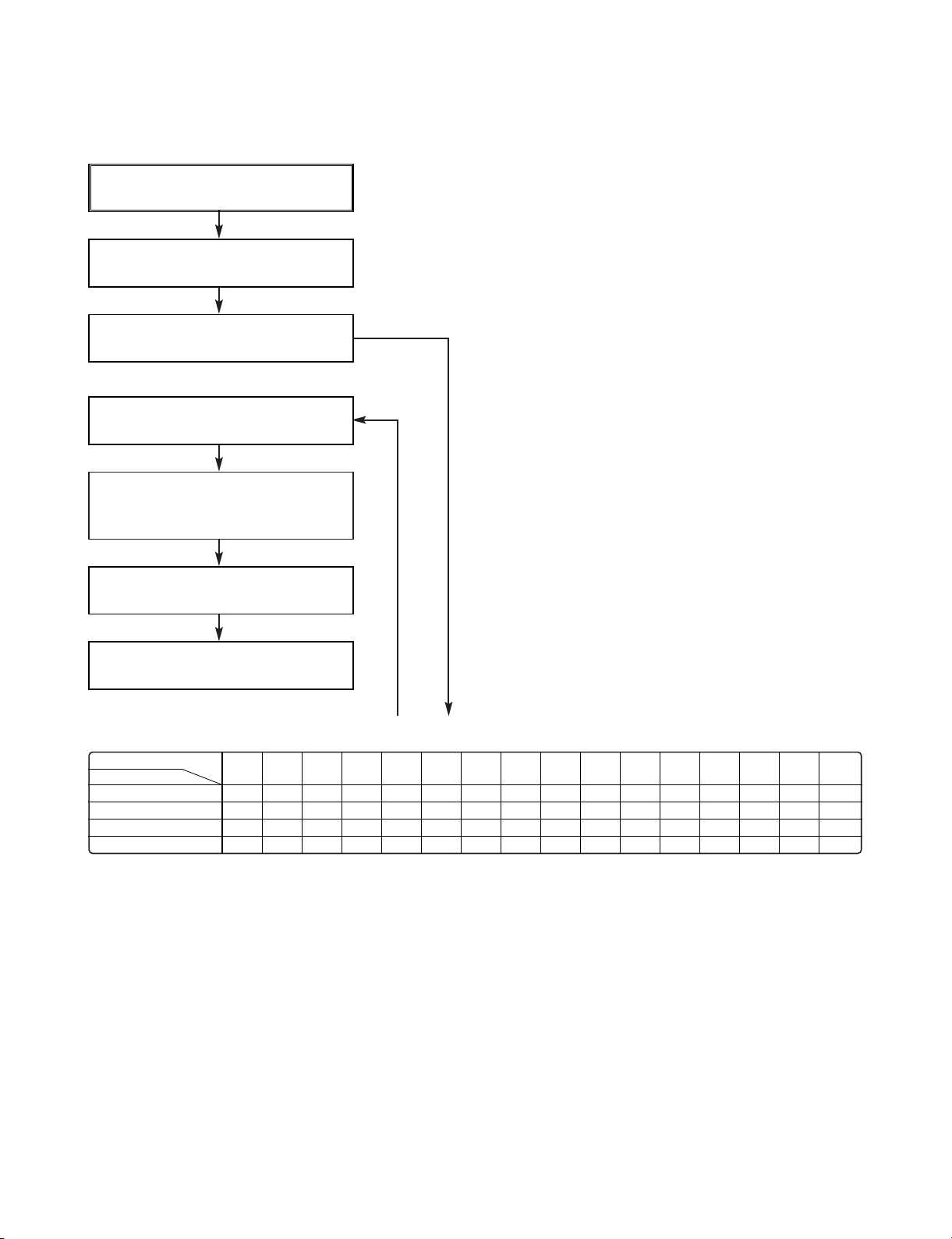
SCL
GND
PD1
EHBDA VIN
T1
PD2/
VC02
2 3 7
13 12
3. Tu/IF, NICAM & A2 BLOCK DIAGRAM
(From Power)
159
27
731
60
59
93
94
158
872
160
871
151 5.3VA
5.2VT
MOD V.IN
MSP3417
Page 41

3-25 3-26
5. Y/C BLOCK DIAGRAM
(PB MODE)
90
93
96
84V.ENV
87
70
V.H.SW
C.ROTARY
DATA
CLOCK
C.SYNC
V.OUT
(MICOM)
S2 V.OUT
S1 V.OUT
SYNC IN
69 68 67
C-Delay
(1H/2H)
BPF
MAIN
CONV
ACCC LPF
CCD
LPF
ACC
DET
CNC
2521
IC201
LA70100M
IC301
LA71750M
29
18 14
PB FM EQ FM OEM
PB FM
AGC
MAIN
DE EMP
Y-LPF
YNR
SUB LPF
60dB AMP
Y/C MIX
65 63 61
46
43
Y-Delay
79 78
(REC MODE)
80
REC'H'
V.H.SW
C.ROTARY
DATA
CLOCK
C SYNC
V.OUT
MICOM
V.IN4
FRONT
V.IN3
DEC
79 78 76 75 70 69 68 67 65 59 58 54 52
50 V.IN2 S1
V.IN1 TUNER
48
46
43
33
32
31
CLK-IN
2928
4.43MHz
2721
95
94
89
88
Killer C-LPF ACC
BPF
Main
Conv
Main
Conv
DETAIL
ENH
NL
EMPHA
W/D
CLIP
IC301
LA71750M
UP REC
SP REC
(To Drum)
(To Drum)
W/D
CLIP
REC
FM EQ
Y-LPF FBC
AGC
SW
Y-DELAY
KILL DEC
REC APC
VX02 VX02
COMP
AMP
1H/2H
DELAY
YNR
29 16
2 12
IC201 LA70100M
Page 42

3-27 3-28
6. Hi-Fi BLOCK DIAGRAM
IC802
A
B
Hi-Fi/
REC
10 22
16
6
12829
12 20 24
26
IC801
A.OUT
To JACK
37
Hi-Fi PB 'B'
Hi-Fi PB 'A'
Hi-Fi REC
1
2
3
4
5
6
7
10
11
21 22
36 35
16
A.OUT 'L'
A.OUT 'R'
17
AUDIO INPUT
BLOCK
VIDEO INPUT
BLOCK
AUDIO INPUT BLOCK
OSD V. IN
TU V. IN
DVD/R V. IN
DVD A.IN 'L'
DVD A.IN 'R'
TU A.IN 'R'
TU A.IN 'L'
NORMAL AUDIO
OUT(T o A VCP)
NORMAL AUDIO
IN(From AVCP)
Tu A.IN 'L'
Tu A.IN 'R'
DVD A.IN 'L'
DVD A.IN 'R'
AV1 A.IN 'L'
AV1 A.IN 'R'
AV2 A.IN 'L'
AV2 A.IN 'R'
MODULATOR
A.OUT
(To Tu)
Page 43

3-29 3-30
7. SYSTEM BLOCK DIAGRAM
2fsc
R524, R514, R518,
R516, R589, C577,
C576, L501, Q504
LD(+)
LD(-)
L/M CONTROL
R525, R526
IC501
HD6432197A
DVD
VCR DATA IN
VCR DATA OUT
DVD CLK
DAV
OTPB LED 'H'
R/C IN(2W)
NC
CST SW
A.ENV
CANAL DET 'H'
Page 44

3-31 3-32
NOTES) Symbol denotes AC ground.
NOTES) Symbol denotes DC chassis ground.
NOTE) Warning
NOTE) Parts that are shaded are critical
NOTE) With respect to risk of fire or
NOTE) electricial shock.
A B C D E F G H I J K L M N O P Q R ST
CIRCUIT DIAGRAMS
1. POWER(SMPS) CIRCUIT DIAGRAM 1_200W
Switching Error.
IC101 is defective.
Switching Error.
IC104 is defective.
Switching Error.
IC105, 106 are defective.
No Power.
F101 is defective.
No 5.3VA.
D127 is defective.
No 3.8VA.
D127 is defective.
No 13VA.
D126 is defective.
No 33VA.
D125 is defective.
No 32VA.
D122 is defective.
Digitron Error.
D123, ZD121, D124 are defective.
No power.
BD101, TH101 are defective.
IMPORTANT SAFETY NOTICE
WHEN SERVICING THIS CHASSIS, UNDER NO CIRCUMSTANCES SHOULD THE ORIGINAL DESIGN BE
MODIFIED OR ALTERED WITHOUT PERMISSION
FROM THE LG ELECTRONICS CORPORATION. ALL
COMPONENTS SHOULD BE REPLACED ONLY WITH
TYPES IDENTICAL TO THOSE IN THE ORIGINAL CIR-
CUIT. SPECIAL COMPONENTS ARE SHADED ON THE
SCHEMATIC FOR EASY IDENTIFICATION.
THIS CIRCUIT DIAGRAM MAY OCCASIONALLY DIFFER FROM THE ACTUAL CIRCUIT USED. THIS WAY,
IMPLEMENTATION OF THE LATEST SAFETY AND
PERFORMANCE IMPROVEMENT CHANGES INTO
THE SET IS NOT DELAYED UNTIL THE NEW SERVICE
LITERATURE IS PRINTED.
NOTE :
1. Shaded( ) parts are critical for safety. Replace only
with specified part number.
2. Voltages are DC-measured with a digital voltmeter
during Play mode.
Page 45

3-33 3-34
NOTES) Symbol denotes AC ground.
NOTES) Symbol denotes DC chassis ground.
NOTE) Warning
NOTE) Parts that are shaded are critical
NOTE) With respect to risk of fire or
NOTE) electricial shock.
A B C D E F G H I J K L M N O P Q R ST
2. POWER(SMPS) CIRCUIT DIAGRAM 1_400W
Switching Error.
IC101 is defective.
Switching Error.
IC104 is defective.
Switching Error.
IC105, 106 are defective.
No Power.
F101 is defective.
No 5.3VA.
D127 is defective.
No 3.8VA.
D127 is defective.
No 13VA.
D126 is defective.
No 33VA.
D125 is defective.
No 32VA.
D122 is defective.
Digitron Error.
D123, ZD121, D124 are defective.
No power.
BD101, TH101 are defective.
IMPORTANT SAFETY NOTICE
WHEN SERVICING THIS CHASSIS, UNDER NO CIRCUMSTANCES SHOULD THE ORIGINAL DESIGN BE
MODIFIED OR ALTERED WITHOUT PERMISSION
FROM THE LG ELECTRONICS CORPORATION. ALL
COMPONENTS SHOULD BE REPLACED ONLY WITH
TYPES IDENTICAL TO THOSE IN THE ORIGINAL CIR-
CUIT. SPECIAL COMPONENTS ARE SHADED ON THE
SCHEMATIC FOR EASY IDENTIFICATION.
THIS CIRCUIT DIAGRAM MAY OCCASIONALLY DIFFER FROM THE ACTUAL CIRCUIT USED. THIS WAY,
IMPLEMENTATION OF THE LATEST SAFETY AND
PERFORMANCE IMPROVEMENT CHANGES INTO
THE SET IS NOT DELAYED UNTIL THE NEW SERVICE
LITERATURE IS PRINTED.
NOTE :
1. Shaded( ) parts are critical for safety. Replace only
with specified part number.
2. Voltages are DC-measured with a digital voltmeter
during Play mode.
Page 46

3-35 3-36
3. POWER(SMPS) CIRCUIT DIAGRAM 2
A B C D E F G H I J K L M N O P Q R ST
Page 47

3-37 3-38
A B C D E F G H I J K L M N O P Q R ST
EE MODE(VIDEO)
TU MODE (AUDIO)
4. TU/IF, NICAM & A2 CIRCUIT DIAGRAM
Page 48

3-39 3-40
5. A/V CIRCUIT DIAGRAM
1
4
5
2
7
8
13
11
12
2
39
10
6
2
14
A B C D E F G H I J K L M N O P Q R ST
PB SECAM COLOR
REC AUDIO
PB Y+C
PB Y
PB C
REC Y+C
REC Y
REC C
REC SECAM COLOR
PB AUDIO(MONO)
WAVEFORM
Audio Tracking is failed.
IC301 Pin 84 is defective.
EE, PB Screen doesn’t appear.
Q305 is defective.
PB COLOR Signal disappear.
IC301 Pin70 is defective.
PB COLOR Signal disappear.
X301 is defective.
D301or IC301 Pin 80
REC is defective.
PB and Recording is failed.
(IC301 doesn’t operate.)
IC301 Pin 69, 68 are defective.
Normal Audio signal is not recorded.
FL301, Q301, Q306 are defective.
No mono Audio Signal
in PB MODE.
Q302, Q303, Q314
are defective.
Page 49

3-41 3-42
6. Hi-Fi CIRCUIT DIAGRAM
A B C D E F G H I J K L M N O P Q R ST
PB
REC
44 Pin is defective.
Hi-Fi Audio is not appear.
IC801 Pins42, 43 aredefective.
All Audio is not appear.
Page 50

3-43 3-44
7. SCART(JACK) CIRCUIT DIAGRAM
A B C D E F G H I J K L M N O P Q R ST
Page 51

3-45 3-46
8. SYSTEM CIRCUIT DIAGRAM
8
76
3
4
5
5
1
2
9
WAVEFORM
A B C D E F G H I J K L M N O P Q R ST
Q501, Q503 are defective.
µ-COM is unstable.
IC505 is defective.
VCR will not operate.
X501 is defective.
CLOCK SETTING will not operate.
X502 is defective.
µ-COM will not operate.
ES501, ES502, LD501 are
defective.
Auto Rew will not working.
RS501,RS502,Q514,
Q515 are defective.
Auto stop occures.
R575, R576, R577,
R578 are defective.
Deck will not operate.
IC504 is defective.
Reset is defective.
Set dead.
Page 52

3-47 3-48
9. TIMER CIRCUIT DIAGRAM_0TOOL
A B C D E F G H I J K L M N O P Q R ST
Page 53

3-49 3-50
10. TIMER CIRCUIT DIAGRAM_5TOOL / 7TOOL
A B C D E F G H I J K L M N O P Q R ST
Page 54

3-51 3-52
11. TIMER CIRCUIT DIAGRAM_6TOOL
A B C D E F G H I J K L M N O P Q R ST
Page 55

3-53 3-54
WAVEFORM & VOLTAGE SHEET
IC301 Pin 20
PB mode
500mvp-p
IC301 Pins 38,32,31
38, 38
Video in 1Vp-p
IC301 Pin 28
PB/REC mode
4.0Vp-p
IC301 Pin 7
REC mode
1.1Vp-p
IC301 Pin 6
REC mode
2.0Vp-p
IC301 Pin 29
PB mode
2.02Vp-p
IC301 Pin 41
PB mode
400mVp-p
IC301 Pin 64
PB mode
400mVp-p
IC301 Pin 23
PB/REC mode
5Vp-p
IC301 Pin 24
PB/REC mode
5Vp-p
IC301 Pins 71 72
REC mode
340mVp-p
IC301 Pins 51 54
PB mode
300mVp-p
IC301 Pin 63
PB mode
400mVp-p
IC301 Pin 11
PB mode
3.6Vp-p
__
IC301 Oscilloscope Waveform
* IC501 Waveform Photographs
V.HSW
(IC501 Pin 105)
1V/10mS
REC/PB MODE
DV.SYNC
(IC501 PIN 109)
1V/100uS
QUE/REV MODE
CTL(+)
(IC501 Pin 3)
1V/10mS
CTL(-)
(IC501 Pin4)
1V/10mS
DFG/FG
(IC501 PIN 103,104)
1V/10mS
REC/PB MODE
CFG
(IC501 Pin9)
1V/10mS
V.IN
(IC501 Pin 17)
500mV/20uS
V.OUT
(IC501 Pin 19)
500mV/20uS
EE/PB MODE
C.SYNC
(IC501 Pin 111)
1.0V/100uS
EE/PB MODE
Page 56

3-55 3-56
• CIRCUIT VOLTAGE CHART
EE PB REC
MODE
PIN NO.
1
2
3
4
5
6
7
8
9
10
11
12
13
14
15
16
17
18
19
20
21
22
23
24
25
26
27
28
29
30
1
2
3
4
5
6
7
8
9
10
11
12
13
14
15
16
17
18
19
20
21
22
23
2.4
2.3
3.4
2.5
0
0.5
0
0
2.9
2.4
2.1
3.1
4
2.4
3.0
3.2
0
0
2.2
2.1
1.9
0
4.8
4.8
2.3
2.3
2.9
0.1
0.19
2
4.9
0
2.2
pulse
2.1
2.2
2.1
2.1
2.1
2.2
2.2
0
2.1
0
2.1
4.9
2.1
4.9
4.0
0
3.1
2.7
2.7
2.4
2.4
3.4
2.4
0
3.7
0
0
2.9
2.4
2.4
1.8
4
2.4
1.8
3.1
4
3.3
2.2
2.5
2.3
0
4.8
4.8
2.2
2.2
2.7
0.18
0.3
2
4.9
0
2.2
pulse
2.1
2.1
2.1
2.1
2.1
2.1
2.2
0
2.1
0
2.1
0.1
2.1
4.9
3.8
0
1.8
2.6
2.6
2.4
2.4
3.4
2.4
0
0.5
0
0
2.9
2.4
2.4
2.3
3
4
2.4
3.2
0
0.12
2.2
2.3
2.3
0
4.8
4.8
1.5
2.4
2.9
0.18
3.8
2
1
0.8
2.3
0.6
2.3
2.2
2.2
2.2
2.9
2.2
2.2
0
2.2
1
2.2
4.8
2.2
4.9
2.8
0
2
3.4
3.4
IC201
IC301
EE PB REC
MODE
PIN NO.
24
25
26
27
28
29
30
31
32
33
34
35
36
37
38
39
40
41
42
43
44
45
46
47
48
49
50
51
52
53
54
55
56
57
58
59
60
61
62
63
64
65
66
67
68
69
70
71
72
73
74
75
76
77
78
4.9
0.1
1.5
2
4
2.6
0
4.5
4.4
2.9
0
1.8
2.9
1.8
2
9
0
0
4.9
2.4
0
2.4
2.6
4
4.2
2.9
1.9
0
1.9
2.3
1.9
5.2
2.2
1.9
3.6
2.8
1.5
1.8
0
1.8
0
1.7
0
0.2
4.8
4.7
0
3.3
4.9
2
2.4
2.3
2.3
1.5
2.5
4.9
3.3
2.2
2.0
4
2.6
0
4.4
4.4
2
0
1.8
3.5
1.8
2
9
0
0
4.9
2.2
3.9
2.4
2.5
4
4.2
3.6
1.9
0
1.9
2.2
1.9
5.2
2.0
2.3
1.3
2.8
1.5
1.3
0
1.3
0
1.1
0
3.7
4.9
4.8
pulse
0
4.8
3.3
1.6
0.6
0.7
1.5
3.3
4.9
0.12
1.2
2
4
2.6
0
4.5
4.5
1.9
1.8
1.8
3.6
1.8
2
9
0
0
4.9
2.3
2.8
2.5
2.6
4
4.2
3
1.95
0
1.95
2.3
2.2
5.2
2
1.6
2.2
2.8
1.4
1.3
0
1.6
0
1.1
0
0.4
4.8
4.8
2.6
0
4.8
2.2
2.3
2.3
2.3
1.5
2.5
EE PB REC
MODE
PIN NO.
79
80
81
82
83
84
85
86
87
88
89
90
91
92
93
94
95
96
97
98
99
100
1
2
3
4
5
6
7
8
9
10
11
12
13
14
15
16
17
18
19
20
21
22
23
24
25
26
27
28
29
30
31
32
1.8
0.9
1.0
0
pulse
0.5
0
0.27
0.7
0.7
0.7
0.7
4.9
0
1.7
1.7
1.7
1.7
0
2.2
2.2
2.2
0
2.6
2.6
2.6
2.6
2.6
2.7
2.58
4.52
5.2
1.8
1.8
2.0
0.26
0.27
1.9
2.47
4.93
2.26
0
2.3
2.3
0
0.52
0.078
5.2
4.5
0
0
0
0
0
1.7
0.9
1
0
0
2.6
0
0.3
0.7
0.7
0.7
0.7
4.9
0
1.7
1.7
1.7
1.7
0
2.2
2.2
2.2
0
2.6
2.6
2.6
2.6
2.6
2.7
2.5
2.2
5.2
1.8
1.8
2.1
3.9
pulse
1.9
1.4
0
0
0
0
2.3
0
2.6
3.1
0
4.5
5.2
0
0
0
0
2.5
4.6
1
0
0
0
1.3
2
0.7
0.7
0.7
0.7
4.8
0
4
4
4
4
0
2.2
2.2
2.2
0
2.6
3.5
1.3
2.6
2.6
2.7
2.5
2.2
5.2
1.7
0
2
0.4
0.16
1.8
2.4
4.8
1.7
0
2.3
2.2
0
0
0.16
5.2
4.5
5.2
0
0
0
0
EE PB REC
MODE
PIN NO.
33
34
35
36
37
38
39
40
41
42
43
44
45
46
47
48
49
50
51
52
53
54
55
56
57
58
59
60
61
62
63
64
65
66
67
68
69
70
71
72
73
74
75
76
77
78
79
80
81
82
83
84
85
86
87
0.18
0.26
5.2
5.2
4.8
4.8
0.21
5.18
3.1
0
0
0
0
0
0
0
0
0
0
pulse
pulse
5.2
pulse
5.2
0
0
4.9
4.7
5.1
5.1
5
3.58
2.8
5.1
0
0
0
5.2
5.2
0
0.3
0
0
1.36
0
0
0
0
3.3
5.2
0
0
0
pulse
0
0.18
0
5.2
5.2
0
4.8
0
0
0
0
4.8
0
0
0
0
0
pulse
0
0
0
0
0
0
5.2
0
0
0
0
5.1
0.2
5
3.5
pulse
5.1
0
5.2
5.2
5.2
0
0
5.1
0
0
1.3
0
0
0
0.15
3.3
5.2
2.5
2.7
3.5
pulse
pulse
0.16
0.16
5.2
5.2
0
4.8
2.3
0
0
0
4.8
0
0
0
5.1
0
0
0.1
0.1
0.26
0.26
5.1
0
0
0
0
0
4.7
5.1
5.1
5
3.6
0
0.2
5.1
0
5.2
5.2
5.2
0
5.1
0
1.6
1.3
0
2.5
0
0
3.3
0
2.5
2.7
3.6
2.8
3.1
EE PB REC
MODE
PIN NO.
88
89
90
91
92
93
94
95
96
97
98
99
100
101
102
103
104
105
106
107
108
109
110
111
112
1
2
3
4
5
6
7
8
9
10
11
12
13
14
15
16
17
18
19
20
21
22
23
24
25
26
27
28
29
4.8
0
0
4.95
0
0
0
0
0
0
0
0
0
0
0
0
0
0
0
0
0
pulse
pulse
0.26
5.2
5.1
1.5
1.5
0
2.4
2.3
0.2
0
0
0
5.1
4.8
4.7
2.5
2.5
0
pulse
0.23
5.14
0
pulse
5.1
0
0
0
0
0
0
0
4.8
0
4.9
0
0
0
0
0
0
0
5.1
2.5
0
0
0
1.4
pulse
2.5
2.5
0
0
0
0
0
0
5.1
1.5
1.5
0
2.4
2.3
pulse
0
0
0
5.1
4.8
4.7
2.5
2.5
0
pulse
pulse
5.1
0
pulse
5.1
0
0
0
0
0
0
0
4.8
0
0
0
pulse
0
0
0
0
0
5.2
2.6
0
0.29
0
1.38
1.39
2.6
2.6
0
2.7
0
0
0
0
5.1
1.5
1.5
0
2.4
2.3
pulse
pulse
pulse
0
5.1
4.8
4.8
pulse
pulse
pulse
pulse
pulse
5.1
0
pulse
5.1
0
0
0
0
0
0
0
EE PB REC
MODE
PIN NO.
30
31
32
33
34
35
36
37
38
39
40
41
42
43
44
1
2
3
4
5
6
7
8
9
10
11
12
13
14
15
16
17
18
19
20
21
22
23
24
25
26
27
28
29
30
31
32
33
34
35
36
37
38
39
2.8
2.8
0
5.1
4.2
0
2.8
0
0
0
2.8
2.8
2.5
2.4
0
3.8
3.8
3.8
3.8
3.8
3.8
3.8
3.8
3.8
3.8
3.8
0
3.87
0
0
6
6
0
6
6
4.57
3.82
3.86
3.87
3.87
0.8
0
3.84
3.86
0.79
3.87
3.87
3.86
12
0.6
0.63
0.63
0
0
2.8
2.8
0
5.1
4.2
0
2.8
0
0
0
2.8
2.8
2.5
2.4
0
3.8
3.8
3.8
3.8
3.8
3.8
3.8
3.8
3.8
3.8
3.8
0
3.87
0
0
6
6
0
6
6
4.5
3.8
3.8
3.8
3.8
0.8
0
3.8
3.8
0.7
3.8
3.8
3.8
12
0.6
0.6
0.6
0
0
2.8
2.8
0
5.1
4.2
0
2.8
0
0
0
2.8
2.8
2.6
2.4
0
3.8
3.8
3.8
3.8
3.8
3.8
3.8
3.8
3.8
3.8
3.8
0
3.8
0
0
6
6
0
6
6
4.5
3.8
3.8
3.8
3.8
0.8
0
3.8
3.8
0.8
3.9
3.9
3.9
12
4.2
4.2
4.2
4.2
0
IC751
IC801
EE PB REC
MODE
PIN NO.
40
41
42
43
44
1
2
3
4
5
6
7
8
9
10
11
12
13
14
15
16
17
18
19
20
21
22
23
24
25
26
27
28
29
30
31
32
33
34
1
2
3
4
5
6
7
8
9
10
11
12
13
14
5
0
4.7
4.8
0
3
12
2.7
12
2.9
5.7
5.7
0
5.1
5.6
11.4
5.7
0
5.6
0.1
5.6
0
0
0
5.7
5.7
5.7
5.6
5.7
5.7
5.7
5.6
5.2
1.4
2.1
3.5
4.7
4.8
0
3.6
0.1
0.8
0
0.7
0.7
0.1
1.4
3.0
0
1.4
0.1
5.2
2.6
5
0.9
4.7
4.6
3.3
3.1
12
2.7
12
2.9
5.7
5.7
5.6
0
5.6
11.4
5.7
0
5.6
0.1
5.6
0
0
0
5.7
5.7
5.7
5.6
5.7
5.7
5.7
5.6
5.2
1.4
2.3
3.5
4.7
4.8
0
3.1
0.1
0.8
0
0.7
0.7
0.1
1.4
2.8
0
1.5
0.1
5.2
2.6
5
0.9
4.8
4.8
0.7
2.9
12
2.7
12
3
5.7
5.7
5.7
0
5.7
11.5
5.7
1.6
2.7
5.7
0
0
0
5.7
5.7
5.7
5.7
5.7
5.7
5.7
5.7
5.2
2.3
1.8
3.5
3.5
4.8
4.9
0
1.5
2.6
0.85
0
0.85
0.79
2.6
1.5
1.5
0
0
2.6
5.2
1.6
IC802
IC901
IC501
Page 57

3-57 3-58
EE PB REC
MODE
PIN NO.
15
16
0
1.5
0
1.5
0
1.6
EEE
EE Mode PB Mode REC Mode
CCCBBB
Transistor
Q110
Q111
Q112
Q113
Q114
Q115
Q116
Q117
Q118
Q301
Q302
Q303
Q304
Q305
Q306
Q308
Q309
Q501
Q502
Q503
Q504
Q514
Q515
Q5S1
Q751
Q804
-22
5.23
12.1
5.24
33.6
0
5.24
5
0
0
4.9
0.2
0.13
2.5
4.9
2.6
2.9
0
0
5.2
0
0
0
0.36
0
2.6
-21.8
5.24
12
5.24
33.4
0
5.2
5
0
0
4.9
0
0
2.7
4.9
2.8
3.2
0
0
5.23
0
0
0
0
0
2.8
-22
5.23
12.1
5.24
33.5
0
5.2
5
0
0
4.9
-7.8
-7.8
3
1.9
3
3.5
0
0
5.2
0
0
0
0.5
0
3.1
-22
5.1
13.9
5.18
33.5
0
5.2
5.23
0
4.9
0
0
0
0
4.9
0
0
0
3.7
5.2
3.8
5.2
0
2.52
3.8
0
-21.8
5.1
13.5
5.18
33.2
0
5.2
5.24
0
4.9
4.86
0
0
0
4.9
0
0
0
2.4
5.2
3.8
Pulse
Pulse
2.5
3.8
0
-22
5
13.4
5.17
33.3
0
5.2
5.2
0
1.6
-14.4
0
0
0
4.6
0
0
0
2.4
5.2
3.7
Pulse
Pulse
3
3.7
0
-21
0
12.7
4.46
32.8
0.74
4.48
5.7
0.68
0
4.9
0
-0.13
1.8
4.9
1.9
2.3
0.68
0.23
4.5
0.62
0
4.95
0
0
1.9
-21
0
12.7
4.46
32.4
0.74
4.49
5.7
0.67
0
4.25
0.7
0.7
2
4.9
2.1
2.5
0.68
0.23
4.5
0.6
Pulse
Pulse
0
0
2
-21
0
12.7
4.47
32.5
0.74
4.48
5.7
0.68
0.8
4.9
-14.3
-14.3
2.3
2.2
2.4
2.8
0.67
0.2
4.5
0.6
Pulse
Pulse
0
0
2.4
Page 58

3-59 3-60
PRINTED CIRCUIT DIAGRAMS
1. MAIN P.C.BOARD
Page 59

3-61 3-62
2. KEY(LEFT) P.C.BOARD
( 0 TOOL )
( 5 TOOL / 7 TOOL )
( 6 TOOL )
Page 60

3-63 3-64
3. KEY(RIGHT) P.C.BOARD
( 0 TOOL )
( 5 TOOL / 7 TOOL )
( 6 TOOL )
Page 61

3-65 3-66
4. POWER P.C.BOARD
( 0 TOOL )
( 5 TOOL / 6 TOOL / 7 TOOL )
LOCATION GUIDE
Page 62

3-67
ELECTRICAL TROUBLESHOOTING GUIDE
1. System operation flow
Power On
No
Yes
Yes
Yes
No
No
No
Show LOGO
Tray Closed?
Tray Close to Closed position
SLED Moves to Inner Position
Recieve
OPEN/ CLOSE
Key?
Receive
CLOSE Key?
1. Stop Playback & Open Tray
2. Display tray open message & LOGO
1. Execute Pressed Key & IR Key
2. Systemoperati on Routine Loop
1. Judge whether have disc and disc type
2. Jump to related disc reading procedure
SLED at Inner
Side?
1. 8032 initializes SERVO, DSP & RISC registers
2. Write RISC code to SDRAM
3. Reset RISC
DVD PART
Page 63

3-68
2. SYSTEM Test flow
TEST
Check the AC Voltage
Power PCBA(110V or 220V)
YES
Switch on the Power PCBA
Is the DC Voltage
outputs OK?
(5V,1.8V,3.3V,8V,12V)
YES
Make sure the main PCBA don't
short on VCCs and switch it on.
NO
NO
Replace power PCBA or
AC transformer.
Repair or Replace Power PCBA
Is 3.3V and 1.8V DC
outputs normal on main
PCBA?
YES
Connect to PC RS232 Cable and
update the FLASH memory code.
Update FLASH
successfully?
YES
A
NO
NO
Check the regulators or related diodes.
1. Check 27MHz system clock.
2. Check system reset circuit.
3. Check FLASH R/W enable signal PRD,RWR.
4. Check RS232 SIGNALS.
5. Check FLASH Memory related circuit.
Page 64

3-69
A
RESET or Power On.
Show LOGO?
YES
NO
Flash Memory operates
properly?
YES
SDRAM works properly?
YES
MT1389 VIDEO outputs
properly?
YES
Have TV signal output?
YES
Check AV cable connection
to TV set.
NO
NO
NO
NO
Check connection lines between FLASH
& MT1389 and the FLASH access time
whether is suitable or not.
Check connection lines between SDRAM
& MT1389 and the SDRAM is damaged.
Check the related circuit of MT1389.
Check the filtering and amp circuit of
TV signal.
Does Tray move
inside when it is not
at closed position?
YES
B
NO NO
Normal TROUT &TRIN
signals?
YES
Normal TRCLOSE &
TROPEN signal?
YES
Normal LOAD+ & LOAD-
signal?
YES
Check the cable connection between
main PCBA and loader.
NO
NO
Check the load OPEN & CLOSE
Check the Tray control IO pins on
Check the Tray control amplifying
switch
MT1389 & IP4504.
circuit on Motor driver.
Page 65

3-70
B
Does the SLED move
to inner side when it is at
outter position?
YES
Do not put in disc and tray
close.
NO NO
Motor Driver STBY
Pin is High?
YES
Is FMSO DC Level higher
than 1.4V?
YES
SL+ and SL- output
properly?
YES
Check the cable connection with
MECHA.
NO
NO
Check the connection line of
STBY signal.
Check the related circuit of
FMSO.
Check the amp circuit on motor
driver.
Optical Lens has
movements for searching
Focus?
YES
C
NO NO
Proper FOSO outputs
to motor driver?
YES
Proper F+ & F- outputs?
YES
Check cable connect on with
pick-up head.
NO
Check FOSO connection on
MT1389 and motor dirver.
Check the amp circuit on motor
dirver.
Page 66

3-71
C
Laser turns on when
reading disc?
YES
Put disc in? Laser off
YES
Disc ID is correct?
YES
NO NO
NO
NO NO
LD01 or LD02 output
Collector voltage of
power transistor is OK?
Check cable connection between
transistor ouput and pick-up
Proper RFL signal
properly?
YES
YES
head.
on MT1389?
YES
NO
Check the laser power circuit
on MT1336 and connecting to
power transistor.
Check the related circuit on
laser power transistor
Check the related circuit
on MT1389 RFL signal.
Does spindle rotate?
YES
D
Check LDO1 & LDO2 signal
NO NO
Proper DMSO signal on
MT1389
YES
SP+ & SP- output
properly?
YES
Check the cable connection
between spindle and main PCBA.
NO
Check DMSO related
circuit on MT1389.
Check the spindle control
amp circuit of motor
driver.
Page 67

3-72
D
YES
Focus ON OK?
YES
Track On OK?
YES
NO
NO
Proper signals on
A,B,C,D of MT1389
YES
Check FEO signal
on MT1389
YES
Check FOSO signal on MT1389
Normal TEO Signal on
MT1389?
YES
Properly TRSO signal
on MT1389?
YES
NO
NO
NO
NO
Check connections between
MT1389 and pick-up head.
Check the FOSO connection on
MT1389 and motor driver.
Check the related
circuit on MT1389
Check the TRSO
connection on MT1389
and motor dirver.
Disc is play ?
YES
E
NO
T+ & T- output
properly?
YES
Check cable connection on
pick-up head.
Check RFO & RFLVL signal waveform.
NO
Check the tracking control
amp circuit on motor
driver.
Page 68

3-73
E
Normal Audio output
when disc playback?
YES
Normal IR.VFD & Front
pannel key functions?
YES
TEST END
NO
NO
Audio DAC received
correct data stream?
YES
Normal Audio DAC
out?
YES
Check Audio filter,amplify,mute
IR.VFD Front pannel key & MT1389
Check the cable connection on
circuit.
Communications between
is normally?
YES
Front pannel.
NO
NO
NO
Check connection between MT1379
&Audio DAC.
Check the related
circuit of Audio DAC.
Check communication lines on
MT1389.
Page 69

DETAILS AND WAVEFORMS ON SYSTEM TEST AND DEBUGGING
1. SYSTEM 27MHz CLOCK, RESET, FLASH R/W SIGNAL
1) MT1389 main clock is at 27MHz(X501)
1.0V, 27MHz
FIG 1-1
2) MT1389 reset is low active
PWR_CTL
5.2VA
M_RESET(FRONT)
RESET Time
FIG 1-2
3-74
Page 70

3-75
3) RS232 waveform during procedure(Downloading)
TXD
RXD
FIG 1-3
4) Flash R/W enable signal during download(Downloading)
FRD
FWR
FIG 1-4
Page 71

3-76
2. SDRAM CLOCK
DCLK = 128MHz, Vp-p=2.2, Vmax=2.7V
FIG 2-1
3. TRAY OPEN/CLOSE SIGNAL
1) Tray open/close waveform
TRIN
TROUT
TROPEN
TRCLOSE
FIG 3-1
Page 72

3-77
4. SLED CONTROL RELATED SIGNAL (NO DISC CONDITION)
FMSO(2.0V/1.4V/1.0V)
STBY(3.3V)
SL+(4.7V/4.0V/2.6V)
SL-(5.3V/4.0V/3.0V)
FIG 4-1
5. LENS CONTROL RELATED SIGNAL(NO DISC CONDITION)
FOSO(1.5V/1.4V/1.3V)
F+(4.0V/3.6V/3.2V)
F-(4.0V/3.6V/3.2V)
FIG 5-1
Page 73

3-78
6. LASER POWER CONTROL RELATED SIGNAL(NO DISC CONDITION)
MDI1(0V/180mV)
LD01(5.0V//3.5V)
LD02(5.0V/3.6V)
FIG 6-1
7. DISC TYPE JUDGEMENT WAVEFORM
F+
FE
RFL
FIG 7-1 (DVD)
Page 74

3-79
F+
FE
RFL
FIG 7-2 (DVD)
F+
FE
RFL
FIG 7-3 (CD)
Page 75

3-80
F+
FE
RFL
FIG 7-4 (CD)
8. FOCUS ON WAVEFORM
FE
FOSO
F+
F-
FIG 8-1 (DVD)
Page 76

3-81
FE
FOSO
F+
F-
FIG 8-2 (CD)
9. SPINDLE CONTROL WAVEFORM (NO DISC CONDITION)
DMSO(1.4V/1.8V)
SP-(3.6V/2.4V)
SP+(3.6V/4.8V)
FIG 9-1
Page 77

3-82
10. TRACKING CONTROL RELATED SIGNAL(System checking)
TE
TRSO
T-
T+
FIG 10-1(DVD)
TE
TRSO
T-
T+
FIG 10-2(CD)
Page 78

3-83
11. MT1389 AUDIO OPTICAL AND COAXIAL OUTPUT(SPDIF)
FIG 11-1
12. MT1389 VIDEO OUTPUT WAVEFORM
1) 100%
FIG 12-1
Page 79

3-84
13. MT1389 AUDIO OUTPUT TO AUDIO DAC
2) COMPOSITE VIDEO SIGNAL
FIG 12-2
FIG 13-1
Page 80

3-85
FIG 14-1
14. AUDIO OUTPUT FROM AUDIO DAC
Page 81

3-86
1)
• R311 → FRONT L
2)
• R303 → FRONT R
3)
• R309 → SURROUND L
4)
• R301 → SURROUND R
5)
• R307 → CENTER
6)
• R305 → WOOFER
15. DVD & AMP WAVEFORMS
Page 82

3-87
BLOCK DIAGRAMS
1. Overall Block Diagram_200W
TU101
KST-ML001MV0-60L
RADIO TUNER MODULE
AVCC, APC
M
M
PICK
UP
SPINDLE
MOTOR
SLED
MOTOR
M
LOADING
MOTOR
DP-7C
IC402
IP4504A
MOTOR DRIVER
SL+, SL-
LOAD+, LOAD-
SP+, SP-
F+, F-, T+, T-
RVCC2, +P8V
LD01, LD02, IOA,
V2.0, MDI1
CD : RFO, A, B, C, D, E, F
DVD : RFO, A, B, C, D
TROUT, TRIN, ADIN
LIMIT
V1P4
IC501
MT1389DEC
MPEG & DSP
TROPEN, TRCLOSE, TRSO, FOSO, DMSO, FMSO, STBY
IC5A1
A29LV800TA-70
1M, 8BIT
FLASH
DV33
IC506
M12L64164A
64Mb, SDRAM
SD33
AD[0:7]
A[00:21]
PCE#, PRD#, PWR#
MA[00:11]
DQ[00:15]
DQM[0:1]
DCS#, DRAS#, DCAS#,
DWE#
BA[0:1], SDCLK, SDCKE
IC505
KS24C021CS
2Kb,
EEPROM
DV33
SDA
SCL
J501
RS-232
X501
27MHz
TXD
RXD
AV33, DV33
PDV03
CONTROL
SIGNAL
DVD_ENA, CLK, DATAIN
DVD_RESET
URST
DVD_DATAOUT
IC507
MM1623XFBE
VIDEO 6dB AMP
5V
AMP_ENA, CLK, DATAOUT
AMP_DATAIN
PDV02
ANA LOG A/V SIGNAL
AUDIO_L, R
LINE2, LINE3
DVD_L, R
CVBS
Y_OUT, Y_G, P_B, P_R
JK601
S-VIDEO
Y_OUT, C_OUT
Y[1:6]
D2-T1, T2, T3
IC101
LC875700B
AUDIO MICOM
REG_5VA
X101
9.8304MHz
IC730,
IC750
STA508
REG_3.3VA, 32VA
L.P.F
S.L
F.L
C
SW
F.R
S.R
L712
L711
L713
L716
L715
L714
JKS01
SPEAKER TERMINAL
505_FAULT, TH_WAR
505_PDN
IC301
PS9818
8CH. PWM
MODULATO R
REG_3.3VA
SL+/
FL+/
C+/
SW+/
FR+/
SR+/
X201
12.288MHz
PS9818_CLK, RESET, PDN
PS9818_DATA
REG-9V
RDS_CLK, DATA
OPTION
P_CE, P_CLK, P_DO
P_DI
MUTE
PN102
DL JIG
DLCLK, DLCE
DLVDD
DLRST, DLDATA
IC205
OPAMP
A_MUTE
FRONT, REAR, C/SW
DALRCK, DABCK
DN_MIX
IC203
MM1231
AUDIO S/W
IC204
OPAMP
IC206
CS5331A
6Ch. ADC
AMCLK
ADATA
Q607, Q608
REG_5VA
TUN_L, R
AUDIO_L, R
1231_CTRL
REG_9V
R135, R136
DN_MIX+/
JK602
OPT.
SPDIF
RIN, LIN
SBCK, SLRCK
Page 83

3-88
2. Overall Block Diagram_400W
IC506
SD33
IC5A1
A29LV800TA-70
1M, 8BIT
DV33
FLASH
J501
RS-232
AD[0:7]
A[00:21]
DWE#
DCS#, DRAS#, DCAS#,
BA[0:1], SDCLK, SDCKE
DQ[00:15]
DQM[0:1]
M12L64164A
64Mb, SDRAM
MA[00:11]
PCE#, PRD#, PWR#
AV33, DV33
TXD
IC501
MT1389DEC
KS24C021CS
DV33
EEPROM
RXD
MPEG & DSP
IC505
2Kb,
SCL
27MHz
SDA
X501
PDV03
CONTROL
SIGNAL
DVD_DATAOUT
DVD_ENA, CLK, DATAIN
URST
ADATA
ALRCK, ABCK
AMCLK
IC204
OPAMP
DVD_RESET
AMP_ENA, CLK, DATAOUT
JK602
OPT.
AMP_DATAIN
REG_5VA
DN_MIX
DALRCK, DABCK
FRONT, REAR, C/SW
SPDIF
D2-T1, T2, T3
Y[1:6]
IC202
AK4586
ANA LOG A/V SIGNAL
AUDIO_L, R
LINE2, LINE3
6Ch. CODEC
RIN, LIN
PDV02
DVD_L, R
S-VIDEO
CVBS
Y_OUT, Y_G, P_B, P_R
5V
IC507
MM1623XFBE
VIDEO 6dB AMP
IC205
OPAMP
DN_MIX+/
JK601
Y_OUT, C_OUT
Q607, Q608
A_MUTE
12.288MHz
X201
CD : RFO, A, B, C, D, E, F
DVD : RFO, A, B, C, D
SPINDLE
DP-7C
UP
PICK
M
MOTOR
LD01, LD02, IOA,
LOADING
SLED
V2.0, MDI1
MOTOR
MOTOR
M
M
AVCC, APC
F+, F-, T+, T-
LOAD+, LOAD-
LIMIT
SP+, SP-
SL+, SL-
IC301
C+/
L742
S.L
IC710, 730
L731
L762
C
F.L
PS9818
8CH. PWM
MODULATO R
STA505
IC750, 770
L771,781
SW
JKS01
L722
F.R
FR+/
SR+/
SW+/
L711
S.R
SPEAKER TERMINAL
OVERALL BL OCK DIA GRAM
REG_9V
V1P4
TROUT, TRIN, ADIN
TROPEN, TRCLOSE, TRSO, FOSO, DMSO, FMSO, STBY
IC402
IP4504A
MOTOR DRIVER
RVCC2, +P8V
TUN_L, R
R135, R136
IC203
MM1231
9.8304MHz
AUDIO_L, R
X101
AUDIO S/W
1231_CTRL
REG_5VA
MUTE
PS9818_DATA
PS9818_CLK, RESET, PDN
IC101
LC875700B
AUDIO MICOM
P_DI
TU101
OPTION
RDS_CLK, DATA
P_CE, P_CLK, P_DO
RADIO TUNER MODULE
KST-ML001MV0-60L
DLCLK, DLCE
DLRST, DLDATA
REG-9V
505_PDN
DLVDD
DL JIG
PN102
REG_3.3VA
FL+/
SL+/
REG_3.3VA, 32VA
505_FAULT, TH_WAR
L.P.F
Page 84

3-89
3. SERVO Block Diagram
ROM
FLASH
AD[0:7]
A[0:20]
X601
27MHz
X-TAL
IC501
EEP
ROM
SCL, SDA
PRD#, PWR#
PCE#
MT1389
ONE CHIP
DVDPLAYER
RS232C(MTK)
RXD, TXD
MA[0:11]
DQM0 ,DQM1
WE#,CAS#,RAS#
CS#,BA0,BA1
SDCLK
SDCKE
IC506
SDRAM
DQ[0:15]
4M x 16bit
ALPC
TRCLOSE
ADIN
IC5A1
IP4504A
STBY,V1P4
FOSO,TRSO,FMSO
DMSO,,TROPEN
Motor Driver
MDI 1
LD0 1, LDO 2, IOA
V20, PICKSEL
DVD: A,B,C,D, RFO
CD: A,B,C,D, E, F,RFO
LIMIT,TRIN,TROUT
F+, F-, T+, T-
SP+, SP-
LOAD+, LOAD-
SL+, SL-
UP
PICK
M/D
Page 85

3-90
4. MPEG & MEMORY Block Diagram
VIDEO
Interface
IC505
EEPROM
Y2(Y),Y3(Color)
Y4(Y),Y5(Cb),Y6(Cr)
ASPECT(16:9)
SCL,SDA
ACLK,ALRCK,ABCK
MUTE,VSCK,VSDA
AUDIO
Interface
ASTB,SCL,SDA
ASDTA[0:3]
ASPDIF
AD[0:7]
IC506
SDRAM
64M
A[0:20]
IC5A1
PWR,PCE,PRD
(16 M )
FLASH MEMORY
CS,DCKE,MA[0:10]
DCLK,WE,CAS,RAS
DQ[0:15]
DQM0,DQM1
MT1389
IC501 (MPEG + DSP + RF)
X501
27MHz
VCR MICOM
Page 86

3-91
5. VIDEO & AUDIO Block Diagram
IC507
VIDEO 6dB
Amp
IC206
AUDIO DAC
(2CH)
IC205
(OP Amp)
LPF&Buffer
CVBS
COMPONENT (R.G.B) / (Y.Pb.Pr )
SUPER VIDEO (Y/C)
(R.G.B) / (Y.Pb.Pr )
(Y/C)
INTERFACE
MPEG
MPEG
AUDIO ‘R’
AUDIO ‘R’
ACLK
ABCK
ALRCK
ADATA3
Page 87

3-92
6. DVD & AMP Block Diagram
FRONT R+-
SURROUND R+ -
FRONT L+-
SURROUND L+-
CENTER
WOOFER
IC710
STA505
IC730
STA505
IC750
STA505
IC770
STA505
IC301
PS9818
IC501
MK1389
IC101
LC875700B
SDA
SCL
RESET
ADATA 0, 1, 2
8BIT micom
100ns(min bus cycle time)
64K/48K-byte ROM
or 128K-byte flash ROM
or 1536/4096-byte RAM
VFD driver
SIO
8- bit 4 ch ADC
Digital Audio Processor
6CH PCM PWM
(24Bit,192kHz)
internal system cl ock : 98.304MHz
external : 12.288MHz (8 PLL)
I/O contr o l r egister (8b i t) : SPI , I2C
data(16 or 24bit)
only AD Mode
Speaker jack
505_PDN
505_TH_WAR
IC202
AK4586
Multi CH audio CODEC
ADC 2CH (Dual bit_wide dinamic range)
DAC 6C H (Multy bit ..)
96kHz,24bit DIR
NON-PCM bit stream detect
control : serial interface
dinamic range : ADC_100 dB , DAC_106dB
Volume control (AC-3)
40V 3.5A
DMOS output stage
50+50W :
THD=10%_30V(8ohm)
80W :
THD=10%_36V(8ohm)
967879
31/32
29/30
2,3/8,9
10,11/16,17
2,3/8,9
10,11/16,17
31/32
29/30
31/32
31,32/
29.30
2,3,8,9/
10,11,
16,17
2,3/8,9
495268
625559
DO
CS
CLK
DI
INT0
INT1
RST
262522
60
32 3443 42 41 23 52
19 1718 16 14 15 44
AMCLK
7
ALRCK
ABCK
ADATA
8
9
10
REAR R
FRONT R
FRONT L
REAR L
CENTER
S/WOOFER
31
30
Analog_L
Analog_R
S/W IC
SPDIF
3
12.288MHz
12.288MHz
AMCLK
ALRCK
ABCK
3
Analog_L
Analog_R
SPDIF IN : AK4586 CS493264 PS9706 speaker
Analog L/R : MM1231 AK4586 NJM4560M DVD L/R
5V
32V
3.3V
1.8V
4.5~5.5V
IC203
MM1231
1231_CTRL
33
11 4 9 14
7
43
41
33
32
215
213
214
209
Tuner or radio tuner
Page 88

A B C D E F G H I J K L M N O P Q R ST
3-93 3-84
CIRCUIT DIAGRAMS
1. MPEG CIRCUIT DIAGRAM
Page 89

A B C D E F G H I J K L M N O P Q R ST
3-95 3-96
2. RF & SERVO CIRCUIT DIAGRAM
Page 90

A B C D E F G H I J K L M N O P Q R ST
3-97 3-98
3. AUDIO, µ_COM CIRCUIT DIAGRAM(DVD & AMP)
Page 91

A B C D E F G H I J K L M N O P Q R ST
3-99 3-100
4. DIGITAL AMP CIRCUIT DIAGRAM (DVD & AMP)_200W
Page 92

4. DIGITAL AMP CIRCUIT DIAGRAM (DVD & AMP)_400W
A B C D E F G H I J K L M N O P Q R ST
3-101 3-102
Page 93

5. PWM & CODEIC CIRCUIT DIAGRAM (DVD & AMP)_200W
A B C D E F G H I J K L M N O P Q R ST
3-103 3-104
Page 94

5. PWM & CODEIC CIRCUIT DIAGRAM (DVD & AMP)_400W
A B C D E F G H I J K L M N O P Q R ST
3-105 3-106
Page 95

6. INTERFACE CIRCUIT DIAGRAM (DVD & AMP)_200W
A B C D E F G H I J K L M N O P Q R ST
3-107 3-108
Page 96

6. INTERFACE CIRCUIT DIAGRAM (DVD & AMP)_400W
A B C D E F G H I J K L M N O P Q R ST
3-109 3-110
Page 97

3-111 3-112
• CIRCUIT VOLTAGE CHART(200W)
STOP PLAY
MODE
PIN NO.
IC101
(AUDIO. MICOM, LC875700B)
1 5.13 5.13
2 0.00 0.00
3 5.00 5.00
4 0.00 0.00
5 0.00 0.00
6 5.17 5.17
7 3.08 2.78
8 3.05 2.97
9 4.95 4.95
10 0.00 0.00
11 4.95 4.95
12 0.00 0.00
13 0.00 0.00
14 0.00 0.00
15 0.00 0.00
16 0.00 0.00
17 0.00 0.00
18 0.00 0.00
19 4.94 4.94
20 2.50 2.50
21 0.00 0.00
22 2.54 2.54
23 0.00 0.00
24 0.00 4.94
25 2.54 2.42
26 4.94 4.94
27 3.27 3.27
28 2.22 2.22
29 3.27 3.27
30 2.22 2.22
31 4.54 4.54
32 4.94 4.94
33 0.00 4.86
34 4.94 4.94
35 0.00 0.00
36 4.94 4.94
37 4.91 4.91
38 4.94 4.94
39 4.83 4.40
40 3.27 2.97
41 0.00 0.00
42 1.72 0.37
43 0.00 0.00
44 2.51 0.32
45 2.51 0.34
46 4.93 4.93
47 2.53 0.41
48 2.48 0.40
49 4.93 4.93
50 2.50 2.43
51 4.93 4.93
52 0.00 0.00
53 4.91 4.91
54 2.56 2.56
STOP PLAY
MODE
PIN NO.
IC103
(RESET IC, KIA7031)
IC203
(AUDIO SW, MM1231)
IC204
(OP AMP, MC4580)
IC205
(OP AMP, NJM4560)
IC301
(PWM IC, PS9818)
55 2.52 2.52
56 0.00 0.00
57 2.44 2.50
58 2.22 2.21
59 4.94 4.94
60 2.54 2.57
61 2.51 2.62
62 0.00 0.00
63 4.94 4.94
64 5.12 5.12
1 3.79 3.79
2 0.00 0.00
3 4.94 4.94
1 5.07 5.02
2 0.00 0.01
3 4.35 4.34
4 0.00 0.00
5 4.35 4.34
6 4.35 4.34
7 4.35 4.34
8 5.08 5.03
9 5.06 5.02
10 0.00 0.00
11 5.07 5.03
12 4.34 4.34
13 9.10 9.10
14 5.05 5.01
15 0.00 0.00
16 5.05 5.01
1 4.88 4.88
2 4.59 4.59
3 4.59 4.59
4 0.00 0.00
5 4.59 4.59
6 4.59 4.59
7 4.89 4.89
8 9.21 9.21
1 4.30 4.30
2 4.30 4.30
3 4.30 4.30
4 0.00 0.00
5 4.30 4.30
6 4.30 4.30
7 4.30 4.30
8 0.00 0.00
1 0.00 0.00
2 0.00 0.00
3 2.31 2.31
4 4.98 4.98
5 3.18 3.18
STOP PLAY
MODE
PIN NO.
6 2.29 2.29
7 0.48 0.48
8 0.00 0.00
9 0.00 0.00
10 3.18 3.18
11 0.00 0.00
12 0.00 0.00
13 2.31 2.31
14 0.00 0.00
15 0.00 0.00
16 0.00 0.00
17 0.00 0.00
18 0.00 0.00
19 1.62 1.62
20 1.62 1.62
21 0.00 0.00
22 3.18 3.18
23 1.18 1.18
24 0.00 0.00
25 0.00 0.00
26 1.19 1.19
27 0.00 0.00
28 0.00 0.00
29 3.18 3.18
30 1.37 1.37
31 1.52 1.52
32 1.58 1.58
33 0.99 0.99
34 2.33 2.33
35 0.00 0.00
36 1.56 1.56
37 1.56 1.56
38 0.00 0.00
39 3.18 3.18
40 1.56 1.56
41 1.56 1.56
42 2.32 2.32
43 0.00 0.00
44 0.00 0.00
45 1.56 1.56
46 1.56 1.56
47 3.18 3.18
48 1.56 1.56
49 1.56 1.56
50 0.00 0.00
51 1.55 1.55
52 1.54 1.54
53 0.00 0.00
54 1.55 1.55
55 1.55 1.55
56 3.18 3.18
57 0.00 0.00
58 1.54 1.54
59 1.54 1.54
60 0.00 0.00
STOP PLAY
MODE
PIN NO.
IC402
(MD DRIVE, IP4504A)
61 1.54 1.54
62 1.54 1.54
63 0.00 0.00
64 0.00 0.00
65 3.18 3.18
66 2.32 2.32
67 1.54 1.54
68 1.54 1.54
69 0.00 0.00
70 1.52 1.52
71 1.52 1.52
72 3.18 3.18
73 0.00 0.00
74 1.52 1.52
75 1.52 1.52
76 3.14 3.14
77 3.18 3.18
78 2.87 2.87
79 4.16 4.16
80 2.34 2.34
81 0.00 0.00
82 3.19 3.19
83 3.19 3.19
84 0.00 0.00
85 0.00 0.00
86 1.60 1.60
87 3.19 3.19
88 1.54 1.54
89 1.38 1.38
90 0.00 0.00
91 2.33 2.33
92 0.00 0.00
93 1.28 1.28
94 3.19 3.19
95 0.00 0.00
96 4.93 4.93
97 0.07 0.07
98 0.06 0.06
99 0.12 0.12
100 0.20 0.20
1 1.37 1.37
2 2.65 2.65
3 2.64 2.64
4 2.65 2.65
5 2.72 2.72
6 2.69 2.69
7 2.67 2.67
8 0.00 0.00
9 1.35 1.35
10 3.58 3.58
11 0.00 0.00
12 0.00 0.00
13 3.94 3.94
14 3.94 3.94
STOP PLAY
MODE
PIN NO.
IC501
(MPEG, MTK1389)
15 2.47 2.47
16 5.46 5.46
17 3.72 3.72
18 4.20 4.20
19 8.00 8.00
20 1.37 1.37
21 1.81 1.81
22 1.37 1.37
23 3.23 3.23
24 5.20 5.20
25 2.54 2.54
26 2.73 2.73
27 2.62 2.62
28 2.65 2.65
10 0
2 1.67 1.67
3 1.67 1.67
4 1.67 1.67
5 1.67 1.67
6 1.67 1.67
7 1.67 1.67
8 1.99 1.99
9 2.0 2.0
10 2.0 2.0
11 2.0 2.0
12 1.40 1.40
13 1.47 1.41
14 1.47 1.47
15 1.44 1.44
16 1.53 1.53
17 1.54 1.43
18 1.96 2.10
19 1.96 2.06
20 0.00 0.18
21 1.05
22 3.24 2.34
23 3.24 3.21
24 3.24 3.22
25 1.51 1.55
26 0.71 1.93
27 0.00 0
28 2.70 2.71
29 1.96 1.96
30 1.37 1.37
31 1.40 1.32
32 1.27 1.33
33 1.27 1.33
34 2.96 2.80
35 3.24 2.78
36 3.03 2.34
37 1.37 2.04
38 1.37 1.33
39 0.00 0
40 1.37 1.37
STOP PLAY
MODE
PIN NO.
41 1.37 1.37
42 1.37 1.4
43 0.00 0
44 1.57 1.57
45 1.57 1.57
46 3.28 3.28
47 2.96 2.84
48 3.28 3.28
49 0.00 0.00
50 3.26 3.24
51 0.00 0.00
52 1.80 1.80
53 1.97 2.12
54 2.00 1.89
55 1.92 1.76
56 2.14 1.45
57 2.02 1.72
58 2.04 2.23
59 1.39 1.50
60 1.12 0.02
61 0.00 0.00
62 0.00 0.00
63 1.89 1.96
64 0.00 0.00
65 3.16 3.15
66 3.28 3.27
67 1.35 0.27
68 1.41 0.62
69 1.14 0.65
70 2.59 3.00
71 0.33 1.30
72 2.19 1.80
73 3.28 3.27
74 1.72 1.71
75 1.99 2.51
76 0.00 0.00
77 0.00 0.00
78 2.00 2.08
79 0.00 0.00
80 3.27 3.27
81 1.27 1.53
82 1.58 1.52
83 0.86 1.23
84 0.69 0.96
85 0.00 0.00
86 1.49 1.30
87 1.69 1.68
88 1.40 1.32
89 0.00 0.00
90 1.17 1.17
91 1.43 1.34
92 0.31 0.31
93 2.05 1.88
94 0.00 0.00
95 3.15 2.61
STOP PLAY
MODE
PIN NO.
96 3.25 3.22
97 1.80 1.80
98 2.51 2.51
99 2.51 2.51
100 3.25 3.25
101 3.25 3.25
102 3.27 3.27
103 3.27 3.27
104 2.58 2.50
105 1.30 1.30
106 2.51 2.51
107 3.27 3.27
108 3.27 3.27
109 0.00 0.00
110 5.18 5.18
111 3.35 2.52
112 2.60 2.60
113 2.40 1.93
114 0.00 0.02
115 0.84 1.00
116 0.00 0.00
117 0.68 1.25
118 0.99 1.07
119 0.00 0.00
120 0.93 1.82
121 1.32 2.35
122 1.80 1.80
123 1.35 1.14
124 0.99 1.13
125 1.13 1.27
126 0.68 1.33
127 3.27 3.27
128 1.46 1.30
129 1.25 1.40
130 1.00 1.30
131 1.34 1.20
132 0.80 0.90
133 0.83 0.95
134 0.00 0.00
135 1.00 1.00
136 3.29 3.28
137 2.39 2.00
138 3.19 3.10
139 2.93 2.70
140 3.12 3.10
141 3.27 3.27
142 2.57 2.57
143 1.54 1.54
144 0.00 0.00
145 1.60 1.60
146 0.06 0.06
147 0.60 0.60
148 0.00 0.00
149 2.36 1.95
150 2.24 2.00
STOP PLAY
MODE
PIN NO.
151 1.42 1.46
152 1.80 1.80
153 0.60 0.37
154 1.48 1.48
155 3.27 3.27
156 1.66 1.66
157 1.23 1.70
158 0.00 0.00
159 0.07 0.00
160 0.05 0.00
161 0.00 0.00
162 1.24 1.43
163 0.00 0.00
164 1.38 1.45
165 1.55 1.59
166 1.43 1.43
167 3.27 3.27
168 3.27 3.27
169 0.77 0.77
170 0.00 0.00
171 2.75 2.90
172 2.75 2.90
173 1.80 1.80
174 3.27 3.27
175 0.00 0.00
176 2.90 2.90
177 3.27 3.27
178 0.00 0.00
179 2.89 2.89
180 0.00 0.00
181 0.00 0.00
182 3.28 3.28
183 0.00 0.00
184 0.00 0.00
185 0.00 0.00
186 0.00 0.00
187 0.00 0.00
188 0.00 0.00
189 3.27 3.27
190 1.23 1.23
191 1.23 1.23
192 2.30 2.30
193 0.00 0.00
194 0.48 0.48
195 3.28 3.28
196 0.69 0.69
197 0.00 0.00
198 2.90 2.90
199 3.27 3.27
200 0.50 0.50
201 0.00 0.00
202 0.70 0.71
203 0.62 0.69
204 3.28 3.28
205 2.90 2.90
STOP PLAY
MODE
PIN NO.
IC505
(EEPROM)
206 3.90 4.20
207 2.90 2.90
208 1.48 1.48
209 1.30 1.30
210 1.64 1.64
211 1.58 1.58
212 3.28 3.28
213 1.63 1.63
214 1.63 1.63
215 1.63 1.63
216 0.00 0.00
217 0.00 1.21
218 0.00 1.15
219 0.00 1.20
220 0.00 0.07
221 1.82 1.82
222 0.00 1.20
223 0.00 0.00
224 0.00 0.00
225 1.64 1.64
226 0.00 0.00
227 1.82 1.82
228 0.67 0.67
229 0.83 0.84
230 1.40 1.40
231 1.41 1.41
232 0.00 0.00
233 0.03 0.00
234 3.24 3.24
235 1.81 1.81
236 1.52 1.66
237 1.76 1.66
238 1.56 1.56
239 3.24 3.24
240 1.36 1.36
241 0.00 0.00
242 1.68 1.68
243 1.11 1.11
244 3.24 3.24
245 1.59 1.59
246 1.37 1.37
247 1.51 1.51
248 1.90 1.90
249 0.00 0.00
250 1.39 1.39
251 1.46 1.46
252 1.52 1.52
253 1.47 1.47
254 1.26 1.26
255 0.90 0.90
256 3.24 3.24
1 0.00 0.00
2 0.00 0.00
3 0.00 0.00
STOP PLAY
MODE
PIN NO.
IC506
(67MB DRAM)
4 0.00 0.00
5 3.27 3.27
6 3.27 3.27
7 0.00 0.00
8 3.27 3.27
1 3.26 3.26
2 1.08 1.48
3 3.27 3.27
4 1.01 1.61
5 1.02 1.60
6 0.00 0.00
7 1.33 1.40
8 0.91 1.02
9 3.26 3.26
10 0.98 0.80
11 0.69 0.73
12 0.00 0.00
13 0.82 0.80
14 3.26 3.26
15 2.39 2.38
16 3.19 3.22
17 2.93 2.95
18 3.12 3.17
19 2.78 2.90
20 1.37 2.87
21 1.64 0.96
22 0.07 0.06
23 0.39 0.61
24 2.35 2.04
25 2.35 2.05
26 1.44 1.46
27 3.27 3.26
28 0.00 0.00
29 0.99 1.40
30 1.46 0.60
31 1.63 1.47
32 1.13 1.42
33 0.02 0.00
34 0.03 0.00
35 0.00 0.00
36 0.07 0.00
37 0.67 0.00
38 1.06 1.68
39 2.73 1.91
40 0.10 0.00
41 0.00 0.00
42 1.40 1.09
43 3.26 3.26
44 1.48 0.94
45 1.44 0.80
46 0.00 0.00
47 1.51 1.34
48 1.50 1.07
49 3.27 3.26
Page 98

3-113 3-114
STOP PLAY
MODE
PIN NO.
IC507
(SW, MN1623)
IC5A1
(16MB FLASH)
50 1.71 1.10
51 2.27 1.26
52 0.00 0.00
53 0.11 1.05
54 0.00 0.00
1 5.18 5.18
2 2.46 2.46
3 5.19 5.19
4 1.31 1.31
5 0.00 0.00
6 1.55 1.55
7 0.00 0.00
8 2.51 2.51
9 0.00 0.00
10 1.55 1.55
11 0.00 0.00
12 2.46 2.46
13 5.19 5.19
14 2.46 2.46
15 0.00 0.00
16 2.52 2.52
17 0.00 0.00
18 2.52 2.52
19 0.00 0.00
20 2.09 2.09
21 2.06 2.06
22 0.00 0.00
23 2.00 2.00
24 0.00 0.00
25 0.00 0.00
26 2.47 2.47
27 0.00 0.00
28 5.19 5.19
1 1.31 0.27
2 1.44 0.7
3 1.25 0.7
4 2.62 3
5 0.46 1.2
6 2.1 1.9
7 1.74 1.82
8 1.96 2.52
900
10 0 0
11 3.27 3.26
12 5.17 5.17
13 3.27 3.27
14 3.27 3.27
15 2.63 2.63
16 0 0
17 1.05 0
18 1.4 1.63
19 2.05 2.25
20 2.04 1.73
STOP PLAY
MODE
PIN NO.
IC730
(AMP, STA505)
21 0.81 1.54
22 0.8 1.75
23 2.36 1.9
24 2.21 2.12
25 1.98 2.09
26 0 0
27 0 0
28 0 0
29 1.45 1.74
30 1.64 1.14
31 0.47 1.48
32 0.85 1.24
33 0.26 0.88
34 1.06 1.08
35 0.7 0.97
36 1.27 1.00
37 3.27 3.26
38 1.49 1.3
39 1.12 1.1
40 1.64 1.72
41 1.18 1.1
42 1.4 1.3
43 1.04 1.17
44 1.42 1.33
45 2.04 1.88
46 0 0
47 0 0
48
1 0.00 0.00
2 17.27 17.27
3 17.27 17.27
4 35.31 35.31
5 0.00 0.00
6 0.00 0.00
7 35.31 35.31
8 17.29 17.29
9 17.29 17.29
10 17.27 17.27
11 17.27 17.27
12 35.31 35.31
13 0.31 0.31
14 0.33 0.33
15 35.31 35.31
16 35.31 35.31
17 35.31 35.31
18 0.00 0.43
19 0.00 0.00
20 0.02 0.00
21 4.98 4.98
22 4.98 4.98
23 3.27 3.27
24 0.00 0.00
25 2.27 2.27
26 2.27 2.27
STOP PLAY
MODE
PIN NO.
27 2.27 2.27
28 3.27 3.27
29 0.30 0.30
30 1.55 1.55
31 1.55 1.55
32 1.55 1.55
33 30.11 30.11
34 30.11 30.11
35 35.31 35.31
36 35.31 35.31
1 0.00 0.00
2 17.27 17.27
3 17.27 17.27
4 35.31 35.31
5 0.00 0.00
6 0.00 0.00
7 35.31 35.31
8 17.29 17.29
9 17.29 17.29
10 17.27 17.27
11 17.27 17.27
12 35.31 35.31
13 0.31 0.31
14 0.33 0.33
15 35.31 35.31
16 35.31 35.31
17 35.31 35.31
18 0.00 0.43
19 0.00 0.00
20 0.02 0.00
21 4.98 4.98
22 4.98 4.98
23 3.27 3.27
24 0.00 0.00
25 2.27 2.27
26 2.27 2.27
27 2.27 2.27
28 3.27 3.27
29 0.30 0.30
30 1.55 1.55
31 1.55 1.55
32 1.55 1.55
33 30.11 30.11
34 30.11 30.11
35 35.31 35.31
36 35.31 35.31
1 0.00 0.00
2 1.80 1.80
3 3.30 3.30
IC750
(AMP, STA505)
IC6V1
(REGULATOR, LD1117A)
Page 99

3-115 3-116
• CIRCUIT VOLTAGE CHART(400W)
STOP PLAY
MODE
PIN NO.
IC101
(AUDIO. MICOM, LC875700B)
1 5.13 5.13
2 0.00 0.00
3 5.00 5.00
4 0.00 0.00
5 0.00 0.00
6 5.17 5.17
7 3.08 2.78
8 3.05 2.97
9 4.95 4.95
10 0.00 0.00
11 4.95 4.95
12 0.00 0.00
13 0.00 0.00
14 0.00 0.00
15 0.00 0.00
16 0.00 0.00
17 0.00 0.00
18 0.00 0.00
19 4.94 4.94
20 2.50 2.50
21 0.00 0.00
22 2.54 2.54
23 0.00 0.00
24 0.00 4.94
25 2.54 2.42
26 4.94 4.94
27 3.27 3.27
28 2.22 2.22
29 3.27 3.27
30 2.22 2.22
31 4.54 4.54
32 4.94 4.94
33 0.00 4.86
34 4.94 4.94
35 0.00 0.00
36 4.94 4.94
37 4.91 4.91
38 4.94 4.94
39 4.83 4.40
40 3.27 2.97
41 0.00 0.00
42 1.72 0.37
43 0.00 0.00
44 2.51 0.32
45 2.51 0.34
46 4.93 4.93
47 2.53 0.41
48 2.48 0.40
49 4.93 4.93
50 2.50 2.43
51 4.93 4.93
52 0.00 0.00
53 4.91 4.91
54 2.56 2.56
STOP PLAY
MODE
PIN NO.
IC103
(RESET IC, KIA7031)
IC203
(AUDIO SW, MM1231)
IC204
(OP AMP, MC4580)
IC205
(OP AMP, NJM4560)
IC301
(PWM IC, PS9818)
IC202
(CODEC, AK4586VQ)
55 2.52 2.52
56 0.00 0.00
57 2.44 2.50
58 2.22 2.21
59 4.94 4.94
60 2.54 2.57
61 2.51 2.62
62 0.00 0.00
63 4.94 4.94
64 5.12 5.12
1 3.79 3.79
2 0.00 0.00
3 4.94 4.94
1 2.77 2.71
2 1.64 1.64
3 4.94 4.86
4 0.00 0.00
5 3.27 3.27
6 0.00 0.00
7 1.46 1.47
8 0.00 1.63
9 0.00 1.60
10 0.00 1.21
11 2.30 2.41
12 0.00 0.86
13 0.00 0.61
14 0.00 0.00
15 0.00 0.00
16 1.40 0.75
17 0.00 0.00
18 0.00 0.00
19 4.94 4.93
20 0.00 0.00
21 0.00 0.00
22 4.95 4.94
23 4.95 4.94
24 2.47 2.45
25 0.00 0.00
26 2.47 2.41
27 2.49 2.40
28 2.50 2.46
29 2.50 2.46
30 2.50 2.46
31 2.50 2.46
32 2.70 2.46
33 3.16 2.46
34 4.95 4.91
35 0.00 1.19
36 0.00 0.00
37 0.00 2.42
38 0.00 0.00
39 0.00 2.42
40 0.00 0.00
STOP PLAY
MODE
PIN NO.
41 0.00 2.42
42 0.00 0.00
43 0.14 0.14
44 4.94 4.94
1 5.07 5.02
2 0.00 0.01
3 4.35 4.34
4 0.00 0.00
5 4.35 4.34
6 4.35 4.34
7 4.35 4.34
8 5.08 5.03
9 5.06 5.02
10 0.00 0.00
11 5.07 5.03
12 4.34 4.34
13 9.10 9.10
14 5.05 5.01
15 0.00 0.00
16 5.05 5.01
1 4.88 4.88
2 4.59 4.59
3 4.59 4.59
4 0.00 0.00
5 4.59 4.59
6 4.59 4.59
7 4.89 4.89
8 9.21 9.21
1 4.30 4.30
2 4.30 4.30
3 4.30 4.30
4 0.00 0.00
5 4.30 4.30
6 4.30 4.30
7 4.30 4.30
8 0.00 0.00
1 0.00 0.00
2 0.00 0.00
3 2.43 2.43
4 4.94 4.94
5 3.28 3.28
6 2.41 2.41
7 1.08 1.08
8 0.00 0.00
9 0.00 0.00
10 3.28 3.28
11 0.00 0.00
12 0.00 0.00
13 2.43 2.43
14 0.00 0.00
15 0.00 0.00
STOP PLAY
MODE
PIN NO.
IC402
(MD DRIVE, IP4504A)
16 0.00 0.00
17 0.00 0.00
18 0.00 0.00
19 1.62 1.62
20 1.61 1.61
21 0.00 0.00
22 3.28 3.28
23 0.00 1.20
24 0.00 0.00
25 0.00 0.59
26 0.00 1.20
27 0.00 0.00
28 0.00 0.00
29 3.28 3.28
30 1.50 1.50
31 1.59 1.59
32 1.62 1.62
33 0.06 0.06
34 2.44 2.44
35 0.00 0.00
36 1.60 1.60
37 1.60 1.60
38 0.00 0.00
39 3.28 3.28
40 1.61 1.61
41 1.61 1.61
42 2.44 2.44
43 0.00 0.00
44 0.00 0.00
45 0.00 0.00
46 0.00 0.00
47 3.28 3.28
48 0.00 0.00
49 0.00 0.00
50 0.00 0.00
51 1.60 1.60
52 1.60 1.60
53 0.00 0.00
54 1.60 1.60
55 3.28 3.28
56 0.00 0.00
57 0.00 0.00
58 1.60 1.60
59 1.60 1.60
60 0.00 0.00
61 1.60 1.60
62 1.60 1.60
63 0.00 0.00
64 0.00 0.00
65 3.28 3.28
66 2.42 2.42
67 1.60 1.60
68 1.60 1.60
69 0.00 0.00
70 1.60 1.60
STOP PLAY
MODE
PIN NO.
IC501
(MPEG, MTK1389)
71 1.60 1.60
72 3.28 3.28
73 0.00 0.00
74 1.60 1.60
75 1.60 1.60
76 3.24 3.24
77 3.28 3.28
78 2.95 2.95
79 4.33 4.33
80 2.42 2.42
81 0.00 0.00
82 3.27 3.27
83 3.27 3.27
84 0.00 0.00
85 0.00 0.00
86 1.64 1.64
87 3.27 3.27
88 1.61 1.61
89 1.55 1.55
90 1.21 1.21
91 2.43 2.43
92 0.00 0.00
93 1.48 1.48
94 3.28 3.28
95 0.00 0.00
96 4.89 4.89
97 0.00 0.00
98 0.00 0.00
99 0.00 0.00
100 0.00 0.00
1 1.37 1.37
2 2.65 2.65
3 2.64 2.64
4 2.65 2.65
5 2.72 2.72
6 2.69 2.69
7 2.67 2.67
8 0.00 0.00
9 1.35 1.35
10 3.58 3.58
11 0.00 0.00
12 0.00 0.00
13 3.94 3.94
14 3.94 3.94
15 2.47 2.47
16 5.46 5.46
17 3.72 3.72
18 4.20 4.20
19 8.00 8.00
20 1.37 1.37
21 1.81 1.81
22 1.37 1.37
23 3.23 3.23
24 5.20 5.20
STOP PLAY
MODE
PIN NO.
25 2.54 2.54
26 2.73 2.73
27 2.62 2.62
28 2.65 2.65
10 0
2 1.67 1.67
3 1.67 1.67
4 1.67 1.67
5 1.67 1.67
6 1.67 1.67
7 1.67 1.67
8 1.99 1.99
9 2.0 2.0
10 2.0 2.0
11 2.0 2.0
12 1.40 1.40
13 1.47 1.41
14 1.47 1.47
15 1.44 1.44
16 1.53 1.53
17 1.54 1.43
18 1.96 2.10
19 1.96 2.06
20 0.00 0.18
21 1.05
22 3.24 2.34
23 3.24 3.21
24 3.24 3.22
25 1.51 1.55
26 0.71 1.93
27 0.00 0
28 2.70 2.71
29 1.96 1.96
30 1.37 1.37
31 1.40 1.32
32 1.27 1.33
33 1.27 1.33
34 2.96 2.80
35 3.24 2.78
36 3.03 2.34
37 1.37 2.04
38 1.37 1.33
39 0.00 0
40 1.37 1.37
41 1.37 1.37
42 1.37 1.4
43 0.00 0
44 1.57 1.57
45 1.57 1.57
46 3.28 3.28
47 2.96 2.84
48 3.28 3.28
49 0.00 0.00
50 3.26 3.24
STOP PLAY
MODE
PIN NO.
51 0.00 0.00
52 1.80 1.80
53 1.97 2.12
54 2.00 1.89
55 1.92 1.76
56 2.14 1.45
57 2.02 1.72
58 2.04 2.23
59 1.39 1.50
60 1.12 0.02
61 0.00 0.00
62 0.00 0.00
63 1.89 1.96
64 0.00 0.00
65 3.16 3.15
66 3.28 3.27
67 1.35 0.27
68 1.41 0.62
69 1.14 0.65
70 2.59 3.00
71 0.33 1.30
72 2.19 1.80
73 3.28 3.27
74 1.72 1.71
75 1.99 2.51
76 0.00 0.00
77 0.00 0.00
78 2.00 2.08
79 0.00 0.00
80 3.27 3.27
81 1.27 1.53
82 1.58 1.52
83 0.86 1.23
84 0.69 0.96
85 0.00 0.00
86 1.49 1.30
87 1.69 1.68
88 1.40 1.32
89 0.00 0.00
90 1.17 1.17
91 1.43 1.34
92 0.31 0.31
93 2.05 1.88
94 0.00 0.00
95 3.15 2.61
96 3.25 3.22
97 1.80 1.80
98 2.51 2.51
99 2.51 2.51
100 3.25 3.25
101 3.25 3.25
102 3.27 3.27
103 3.27 3.27
104 2.58 2.50
105 1.30 1.30
STOP PLAY
MODE
PIN NO.
106 2.51 2.51
107 3.27 3.27
108 3.27 3.27
109 0.00 0.00
110 5.18 5.18
111 3.35 2.52
112 2.60 2.60
113 2.40 1.93
114 0.00 0.02
115 0.84 1.00
116 0.00 0.00
117 0.68 1.25
118 0.99 1.07
119 0.00 0.00
120 0.93 1.82
121 1.32 2.35
122 1.80 1.80
123 1.35 1.14
124 0.99 1.13
125 1.13 1.27
126 0.68 1.33
127 3.27 3.27
128 1.46 1.30
129 1.25 1.40
130 1.00 1.30
131 1.34 1.20
132 0.80 0.90
133 0.83 0.95
134 0.00 0.00
135 1.00 1.00
136 3.29 3.28
137 2.39 2.00
138 3.19 3.10
139 2.93 2.70
140 3.12 3.10
141 3.27 3.27
142 2.57 2.57
143 1.54 1.54
144 0.00 0.00
145 1.60 1.60
146 0.06 0.06
147 0.60 0.60
148 0.00 0.00
149 2.36 1.95
150 2.24 2.00
151 1.42 1.46
152 1.80 1.80
153 0.60 0.37
154 1.48 1.48
155 3.27 3.27
156 1.66 1.66
157 1.23 1.70
158 0.00 0.00
159 0.07 0.00
160 0.05 0.00
STOP PLAY
MODE
PIN NO.
IC505
(EEPROM)
161 0.00 0.00
162 1.24 1.43
163 0.00 0.00
164 1.38 1.45
165 1.55 1.59
166 1.43 1.43
167 3.27 3.27
168 3.27 3.27
169 0.77 0.77
170 0.00 0.00
171 2.75 2.90
172 2.75 2.90
173 1.80 1.80
174 3.27 3.27
175 0.00 0.00
176 2.90 2.90
177 3.27 3.27
178 0.00 0.00
179 2.89 2.89
180 0.00 0.00
181 0.00 0.00
182 3.28 3.28
183 0.00 0.00
184 0.00 0.00
185 0.00 0.00
186 0.00 0.00
187 0.00 0.00
188 0.00 0.00
189 3.27 3.27
190 1.23 1.23
191 1.23 1.23
192 2.30 2.30
193 0.00 0.00
194 0.48 0.48
195 3.28 3.28
196 0.69 0.69
197 0.00 0.00
198 2.90 2.90
199 3.27 3.27
200 0.50 0.50
201 0.00 0.00
202 0.70 0.71
203 0.62 0.69
204 3.28 3.28
205 2.90 2.90
206 3.90 4.20
207 2.90 2.90
208 1.48 1.48
209 1.30 1.30
210 1.64 1.64
211 1.58 1.58
212 3.28 3.28
213 1.63 1.63
214 1.63 1.63
215 1.63 1.63
STOP PLAY
MODE
PIN NO.
IC506
(67MB DRAM)
216 0.00 0.00
217 0.00 1.21
218 0.00 1.15
219 0.00 1.20
220 0.00 0.07
221 1.82 1.82
222 0.00 1.20
223 0.00 0.00
224 0.00 0.00
225 1.64 1.64
226 0.00 0.00
227 1.82 1.82
228 0.67 0.67
229 0.83 0.84
230 1.40 1.40
231 1.41 1.41
232 0.00 0.00
233 0.03 0.00
234 3.24 3.24
235 1.81 1.81
236 1.52 1.66
237 1.76 1.66
238 1.56 1.56
239 3.24 3.24
240 1.36 1.36
241 0.00 0.00
242 1.68 1.68
243 1.11 1.11
244 3.24 3.24
245 1.59 1.59
246 1.37 1.37
247 1.51 1.51
248 1.90 1.90
249 0.00 0.00
250 1.39 1.39
251 1.46 1.46
252 1.52 1.52
253 1.47 1.47
254 1.26 1.26
255 0.90 0.90
256 3.24 3.24
1 0.00 0.00
2 0.00 0.00
3 0.00 0.00
4 0.00 0.00
5 3.27 3.27
6 3.27 3.27
7 0.00 0.00
8 3.27 3.27
1 3.26 3.26
2 1.08 1.48
3 3.27 3.27
4 1.01 1.61
Page 100

3-117 3-118
STOP PLAY
MODE
PIN NO.
IC507
(SW, MN1623)
IC5A1
(16MB FLASH)
IC710
(AMP, STA508)
5 1.02 1.60
6 0.00 0.00
7 1.33 1.40
8 0.91 1.02
9 3.26 3.26
10 0.98 0.80
11 0.69 0.73
12 0.00 0.00
13 0.82 0.80
14 3.26 3.26
15 2.39 2.38
16 3.19 3.22
17 2.93 2.95
18 3.12 3.17
19 2.78 2.90
20 1.37 2.87
21 1.64 0.96
22 0.07 0.06
23 0.39 0.61
24 2.35 2.04
25 2.35 2.05
26 1.44 1.46
27 3.27 3.26
28 0.00 0.00
29 0.99 1.40
30 1.46 0.60
31 1.63 1.47
32 1.13 1.42
33 0.02 0.00
34 0.03 0.00
35 0.00 0.00
36 0.07 0.00
37 0.67 0.00
38 1.06 1.68
39 2.73 1.91
40 0.10 0.00
41 0.00 0.00
42 1.40 1.09
43 3.26 3.26
44 1.48 0.94
45 1.44 0.80
46 0.00 0.00
47 1.51 1.34
48 1.50 1.07
49 3.27 3.26
50 1.71 1.10
51 2.27 1.26
52 0.00 0.00
53 0.11 1.05
54 0.00 0.00
1 5.18 5.18
2 2.46 2.46
3 5.19 5.19
4 1.31 1.31
STOP PLAY
MODE
PIN NO.
5 0.00 0.00
6 1.55 1.55
7 0.00 0.00
8 2.51 2.51
9 0.00 0.00
10 1.55 1.55
11 0.00 0.00
12 2.46 2.46
13 5.19 5.19
14 2.46 2.46
15 0.00 0.00
16 2.52 2.52
17 0.00 0.00
18 2.52 2.52
19 0.00 0.00
20 2.09 2.09
21 2.06 2.06
22 0.00 0.00
23 2.00 2.00
24 0.00 0.00
25 0.00 0.00
26 2.47 2.47
27 0.00 0.00
28 5.19 5.19
1 1.31 0.27
2 1.44 0.7
3 1.25 0.7
4 2.62 3
5 0.46 1.2
6 2.1 1.9
7 1.74 1.82
8 1.96 2.52
900
10 0 0
11 3.27 3.26
12 5.17 5.17
13 3.27 3.27
14 3.27 3.27
15 2.63 2.63
16 0 0
17 1.05 0
18 1.4 1.63
19 2.05 2.25
20 2.04 1.73
21 0.81 1.54
22 0.8 1.75
23 2.36 1.9
24 2.21 2.12
25 1.98 2.09
26 0 0
27 0 0
28 0 0
29 1.45 1.74
30 1.64 1.14
STOP PLAY
MODE
PIN NO.
31 0.47 1.48
32 0.85 1.24
33 0.26 0.88
34 1.06 1.08
35 0.7 0.97
36 1.27 1.00
37 3.27 3.26
38 1.49 1.3
39 1.12 1.1
40 1.64 1.72
41 1.18 1.1
42 1.4 1.3
43 1.04 1.17
44 1.42 1.33
45 2.04 1.88
46 0 0
47 0 0
48
1 0.00 0.00
2 15.60 15.60
3 15.60 15.60
4 31.59 31.59
5 0.00 0.00
6 0.00 0.00
7 31.59 31.59
8 15.62 15.62
9 15.62 15.62
10 15.62 15.62
11 15.62 15.62
12 31.59 31.59
13 0.00 0.00
14 0.00 0.00
15 31.59 31.59
16 15.61 15.61
17 15.61 15.61
18 NC NC
19 0.00 0.00
20 0.02 0.02
21 5.02 5.02
22 5.02 5.02
23 3.24 3.24
24 0.00 0.00
25 3.15 3.15
26 3.15 3.15
27 3.15 3.15
28 3.24 3.24
29 1.58 1.58
30 1.58 1.58
31 1.58 1.58
32 1.58 1.58
33 26.30 26.30
34 26.30 26.30
35 31.58 31.58
36 31.58 31.58
IC750
(AMP, STA508)
IC730
(AMP, STA508)
STOP PLAY
MODE
PIN NO.
1 0.00 0.00
2 15.60 15.60
3 15.60 15.60
4 31.59 31.59
5 0.00 0.00
6 0.00 0.00
7 31.59 31.59
8 15.62 15.62
9 15.62 15.62
10 15.62 15.62
11 15.62 15.62
12 31.59 31.59
13 0.00 0.00
14 0.00 0.00
15 31.59 31.59
16 15.61 15.61
17 15.61 15.61
18 NC NC
19 0.00 0.00
20 0.02 0.02
21 5.02 5.02
22 5.02 5.02
23 3.24 3.24
24 0.00 0.00
25 3.15 3.15
26 3.15 3.15
27 3.15 3.15
28 3.24 3.24
29 1.58 1.58
30 1.58 1.58
31 1.58 1.58
32 1.58 1.58
33 26.30 26.30
34 26.30 26.30
35 31.58 31.58
36 31.58 31.58
1 0.00 0.00
2 15.60 15.60
3 15.60 15.60
4 31.59 31.59
5 0.00 0.00
6 0.00 0.00
7 31.59 31.59
8 15.62 15.62
9 15.62 15.62
10 15.62 15.62
11 15.62 15.62
12 31.59 31.59
13 0.00 0.00
14 0.00 0.00
15 31.59 31.59
16 15.61 15.61
17 15.61 15.61
STOP PLAY
MODE
PIN NO.
IC770
(AMP, STA508)
STOP PLAY
MODE
PIN NO.
36 31.58 31.58
1 0.00 0.00
2 1.80 1.80
3 3.30 3.30
IC6V1
(REGULATOR, LD1117A)
18 NC NC
19 0.00 0.00
20 0.02 0.02
21 5.02 5.02
22 5.02 5.02
23 3.24 3.24
24 0.00 0.00
25 3.15 3.15
26 3.15 3.15
27 3.15 3.15
28 3.24 3.24
29 1.58 1.58
30 1.58 1.58
31 1.58 1.58
32 1.58 1.58
33 26.30 26.30
34 26.30 26.30
35 31.58 31.58
36 31.58 31.58
1 0.00 0.00
2 15.60 15.60
3 15.60 15.60
4 31.59 31.59
5 0.00 0.00
6 0.00 0.00
7 31.59 31.59
8 15.62 15.62
9 15.62 15.62
10 15.62 15.62
11 15.62 15.62
12 31.59 31.59
13 0.00 0.00
14 0.00 0.00
15 31.59 31.59
16 15.61 15.61
17 15.61 15.61
18 NC NC
19 0.00 0.00
20 0.02 0.02
21 5.02 5.02
22 5.02 5.02
23 3.24 3.24
24 0.00 0.00
25 3.15 3.15
26 3.15 3.15
27 3.15 3.15
28 3.24 3.24
29 1.58 1.58
30 1.58 1.58
31 1.58 1.58
32 1.58 1.58
33 26.30 26.30
34 26.30 26.30
35 31.58 31.58
 Loading...