

Page 1
LH5PV8512
CMOS 4 M (51 2K × 8 ) Pseudo-Static RAM
FEATURES
•• 524,288 words × 8 b it organ izatio n
•• CE acce ss time ( t
CEA
): 120 ns (MAX.)
•• Cycle ti me (t
RC
): 190 ns (MIN.)
•• Power supp ly :
+3.0 V ± 0.15 V (Operating )
+2.2 V to +3.15 V (Data retention)
•• Power consu mption (MAX.):
126 mW (Operatin g)
95 µW (Standby = CMOS input level )
221 µW (Self-refresh = CMOS input level )
•• Available for address refresh,
auto-refres h, a nd se lf-re fresh mode s
•• 2,048 refresh cycle s/32 ms
•• Addres s non -multip le
•• Not design ed or ra ted as radiation
hardene d
•• Packa ge:
32-pi n , 525 -mil S OP
•• Package materi al: Plastic
•• Substrate material: P-type silicon
•• Process : Silicon-g ate CMOS
•• Operatin g temperature: 0 - 70°C
DESCRIPTION
The LH5PV8512 is a 4M bit Pseudo-Static RAM with
a 524,288 word × 8 bit organization. It is fabricated
using silicon-gate CMOS process technology.
A PSRAM uses on-chip refresh circuitry with a DRAM
memory cell for pseudo-static operation which el iminates external clock inputs, while having the same
pinout as industry standa rd SRAMs. Moreover, due to
the functional similarities between PSRAMs and
SRAMs, existing 512K × 8 SRAM sockets can be filled
with the LH5P V8512N with li ttle or no changes. The
advantage is the cost saving rea lized with the lower
cost PSRAM.
The LH5PV8512 has the ability to fill the gap between
DRAM and SRAM by offering low cost, low power
standby and simple interface.
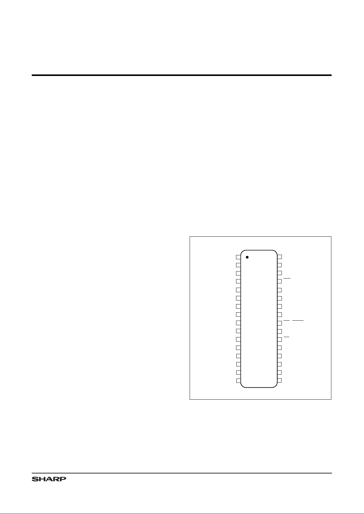
PIN CONNECTIONS
TOP VIEW
1
2
3
4
5
6
9
10
A
2
A
5
Vcc
28
27
26
25
24
23
20
17
A
7
A
6
7
8
A
3
A
4
22
21
A
14
A
12
A
13
A
8
A
11
A
10
CE
I/O
7
I/O
6
I/O
3
11
12
13
32
31
30
29
WE
A
1
14
15
16
19
I/O
5
18
I/O
4
I/O
1
I/O
2
V
SS
A
0
I/O
0
A
9
A
16
A
18
OE/RFSH
5PV8512-1
32-PIN SOP
A
17
A
15
Figure 1. Pin Connections
1
Page 2
PIN DESCRIPTION
PIN NAME FUNCTION
A0 - A
18
Addre ss input
WE Write e nab le inp ut
OE/RFSH
Outpu t e nab le i np ut
Refre sh contro l input
PIN NAME FUNCTION
CE
Chip e nab le inp ut
I/O0 - I/O
7
Data i npu t/o utp ut
V
CC
Power sup ply
GND Ground
I/O
1
CLOCK
GENERATOR
CE
A
12
A
13
A
14
A
3
A
4
A
5
A
6
A
7
A
8
A
9
A
11
A
10
A
2
A
1
A
0
COLUMN
ADDRESS
BUFFER
ROW
ADDRESS
BUFFER
REFRESH
ADDRESS
COUNTER
DATA
IN
BUFFER
DATA
OUT
BUFFER
I/O
SELECTOR
COLUMN
DECODER
SENSE
AMPS
MEMORY
ARRAY
ROW
DECODER
EXT/INT
ADDRESS
MUX.
REFRESH
CONTROLLER
REFRESH
TIMER
I/O
2
I/O
3
I/O
4
I/O
5
I/O
6
I/O
7
V
BB
GENERATOR
V
CC
A
15
A
16
5PV8512-2
I/O
0
12
11
10
9
8
7
6
5
27
26
23
25
4
28
3
31
2
22
16
32
13
14
15
17
18
19
20
21
OE/
RFSH
24
A
17
30
A
18
1
WE 29
V
SS
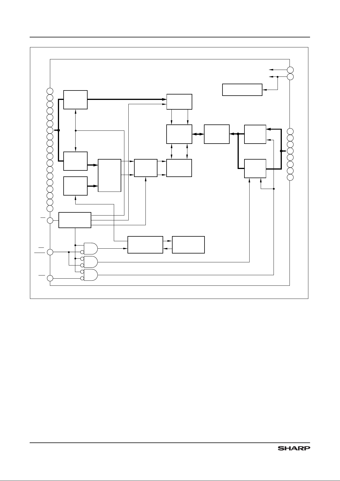
Figure 2. LH5PV8512 Block Diagram
LH5PV8512 CMOS 4M (512K × 8) Pseudo-Static R AM
2
Page 3

TRUTH TABLE
CE OE/RFSH WE I/O
0 - 7
MODE
L L H Output data Read
L X L Input data Write
L H H High-Z
CE only refresh
H L X High-Z Auto-refresh
H H X High-Z Standby
NOTES:
1. X = H or L
2. I f
RF SH = L, it is necessary to meet t
OEH
and t
OCD
.
ABSOLUTE MAXIMUM RATINGS
PARAMETER SYMBOL RATING UNIT NOTE
Appli ed v ol tage on al l p ins V
T
-0.5 to +4.6 V 1
Operat ing te mpe ratu re T
OPR
0 to +70
°C
Storag e t emp era ture T
STG
-65 to +150
°C
Output sh ort ci rcu it c urr ent
I
O
50 mA
Power dis sipati on P
D
600
mW
NOTE:
1. The maximum applicable voltage on any pin with respect to V
SS
.
RECOMMENDED DC OPERATING CONDITIONS (TA = 0 to +70°C)
PARAMETER SYMBOL MIN. TYP. MAX. UNIT NOTE
Suppl y v olt age
V
CC
2.85 3.0 3.15 V 1
V
SS
00 0 V
Input vol tage
V
IH
2.4
4.5 V
V
IL
-0.5 0.6 V
NOTE:
1. When t he supply voltage falls down under the above recommended supply voltage by temporarily power-down, a wait time longer than
400 ms is necessary at VCC = 0 V before the next po wer-up. Af ter the supply voltage rises and gets stable, a pause of 100 µs wit h
CE = RFSH = VIH and 8 dummy cycles are also necessary after the rises.
PIN CAPACITANCE (TA = +25°C, f = 1 MHz, VCC = 3.0 V)
PARAMETER CONDITIONS S YMBOL MIN. MAX. UNIT NOTE
Input cap acitan ce
A
0
- A
18
C
IN1
8pF1
WE, OE/RFSH C
IN2
8pF1
CE C
IN3
8pF1
Input/ out put ca pac ita nce I/O
0
- I/O
7
C
OUT1
10 pF 1
NOTE:
1. Th is parameter is samp led and not 100% tested.
CMOS 4M (512K × 8) Pseud o -S tatic RAM LH5PV8512
3
Page 4

DC ELECTRICAL CHARACTERISTICS (TA = 0 to +70°C, VCC = 3.0 V ± 0.15 V)
PA RA METER SYMBOL CONDITIONS MIN. MAX. UNIT NOTE
Average su ppl y c urr ent in no rmal
operat ion
I
CC1
tRC = 190 ns 40 mA 1
Average su ppl y c urr ent in st and by
mode
I
CC2
CE, OE, RFSH = VIH
0.5 mA
CE, OE, RFSH = VCC - 0.2 V 30 mA
Average su ppl y c urr ent in se lf-r efr esh
cycle
I
CC3
CE = VIH
OE/RFSH = V
IL
0.5 mA
CE = VCC - 0.2 V,
OE, RFSH = 0.2 V
70 mA
Input lea kag e c urr ent I
LI
0 V ≤ VIN ≤ VCC + 0.3 V
0 V on all other pins
-5 5 µA
I/O le aka ge cur ren t
I
LO
0 V ≤ V
OUT
≤ VCC + 0.3 V
Input/output pins in High-Z
-5 5 µA
Output HI GH vol tag e V
OH
I
OUT
= -1 mA 2.4
V
Output LO W v olt age V
OL
I
OUT
= 2.1 mA
0.4 V
NOTE:
1. The in put/output pins are in high impedance state. I
CC1
depends on the cycle time.
LH5PV8512 CMOS 4M (512K × 8) Pseudo-Static R AM
4
Page 5

AC ELECTRICAL CHARACTERISTICS
1, 2, 3, 4, 5
(TA = 0 to +70°C, VCC = 3.0 V ± 0.15 V)
PARAMETER SYMBOL MIN. MAX. UNIT NOTES
Random re ad, wri te cyc le tim e t
RC
190
ns
Random mo dif y w rite cy cl e ti me t
RMW
250
ns
CE pul se wid th t
CE
120 10,000 ns
CE pre cha rge ti me t
P
70 ns
Addres s s etu p t ime
t
AS
0 ns 6
Addres s h old ti me t
AH
30
ns 6
Read c omm and se tup ti me t
RCS
0
ns
Read c omm and ho ld time t
RCH
0
ns
CE acc es s t ime t
CE A
120 ns 7
OE acces s time
t
OEA
60 ns 7
CE to out put in Low -Z
t
CLZ
20 ns 8
OE to out put in Low -Z t
OLZ
0
ns 8
Write d isa ble to out put in Lo w-Z t
WLZ
5
ns 8
Chip d isa ble to ou tpu t i n Hi gh- Z t
CHZ
0
30 ns 8
Output disable to outp ut in High-Z
t
OHZ
30 ns 8
WE to out put in Hig h-Z
t
WHZ
30 ns 8
OE set up ti me f rom CE t
OES
0
ns
OE hol d t ime fro m CE t
OEH
15
ns
OE setup tim e from chip disa ble t
OCD
0
ns
Write c omma nd pul se wid th t
WP
35 ns
Write c omma nd set up tim e
t
WCS
35 10,000 ns
Write c omma nd hol d t ime t
WCH
120 10,000 ns
Data s etu p t ime fro m w rite di sab le t
DS W
30
ns 9
Data s etu p t ime fro m c hip di sab le t
DSC
30
ns 9
Data h old ti me f rom wri te dis abl e t
DHW
0 ns 9
Data h old ti me f rom ch ip dis abl e
t
DHC
0 ns 9
Transiti on time (r ise an d fa ll) t
T
250ns
Refres h t ime in terv al (2, 048 cy cle ) t
REF
32 ms 10, 13, 14
Auto r efr esh cy cle ti me t
FC
190
ns
Refres h d ela y t ime fro m CE t
RFD
70
ns
Refres h p uls e w idt h ( Aut o re fre sh) t
FAP
80 8,000 ns 11, 15
Refres h p rec har ge time (A uto re fres h)
t
FP
40 ns
Refres h p uls e w idt h ( Sel f re fre sh)
t
FAS
8
ms 11, 12, 13, 14, 15
CE del ay tim e f rom ref res h pr ech arg e
(Self ref resh)
t
FRS
600
ns
DATA RETENTION CHARACTERISTICS
12, 13, 14, 15, 16, 17, 18, 19, 20
(TA = 0 to +70°C)
PARAMETER SYMBOL MIN. MAX. UNIT NOTES
Data r ete ntio n v olt age V
R
2.2 3.15 V
Data r ete ntio n c urr ent
(V
CC
= 3.15 V, CE = VCC - 0.2 V, OE/RFS H = 0 .2 V)
I
CCDR
70
µA
Refres h s etu p t ime t
FS
0 ns
Recov er t ime fro m d ata ret ent ion mo de
t
FR
5 ms
CMOS 4M (512K × 8) Pseud o -S tatic RAM LH5PV8512
5
Page 6

NOTES:
1. AC characteristics are m easur ed at tT = 2 ns.
2. AC characteristics are m easur ed at the follow ing condition:
INPUT VOLTAGE OUTPUT VOLTAGE
V
IH
V
IL
V
OH
V
OL
Input level 2.4 V 0.4 V
Input refe rence lev el
1.4 V 1.4 V
Output ref ere nce le vel
2.0 V 0.8 V
3.
In order to in itialize the circuit,
CE and OE/RFSH should be kept VIH for 100 µ s aft er power-up and f ollowed by at least 8 dummy cycles.
4. I f input signals of opposite phase to the outputs are applied in write cycle,
OE or W E must disable output buffer proir to applying data to
the device and data inputs must be float ing prior t o OE or WE turn ing on outputs buffer.
5. Because a PSRAM operates dynamically like a DRAM, it is recommended to put bypass capacitors between V
CC
and GND to absorb power
supply noise due to the peak current.
6. Address signals are latched in the memory at the falling edge of
CE.
7. M easured with a load equivalent to 50 pF.
8. t
CLZ
, t
OLZ
, t
WLZ
, t
CHZ
, t
OHZ
, and t
WHZ
are sampled, and not 100% teste d. t
CHZ
, t
OHZ
, and t
WHZ
define the time at which the output achieves
the open circuit condition and they are not referenced to output voltage levels.
9. In put data is latched in the memory at the earlier rising edge of CE and WE.
10. CE on ly refresh or auto-refresh i s needed to be executed 2, 048 times w ithin 32 ms.
11. Auto-refresh a nd self-refr esh are def ined by
OE/RFSH pulse width during CE = VIH. If OE/R FS H pu lse w idt h is s hor ter than t
FAP
(MAX.),
the cycle is an auto-refresh cycle and memory cells are refreshed by an inter nal address counter. If
OE/RFSH pulse width is longer than
t
FAS
(MIN.), the cycle is a self-refr esh cycle and memory c ells are refr eshed by an inter nal clock generator automatically.
12.
If
CE only refresh is used during norma l read/write cycles, the first addr ess refr es h must be st arted w ith in 15 µs af ter s elf- refr e sh or data
retention mode ends, and the
CE only refresh must be executed continuously for 2,048 refresh cycles.
13.
If distributed auto-refresh is used during normal read/write cycles, the first auto-ref resh must be started with in 15 µs after s elf-ref resh or
data retent ion mode ends.
14.
If burst auto-ref resh is used during norma l read/write cycles, the first auto-refresh must be started with in 15 µs after self -refres h or data
retention mode ends, and the auto-r efresh m ust be executed continuously for 2,048 refr esh cycles.
15. After 8,000 ns (t
FAP
(MAX.)) from RFSH falling, the memory resets its internal address counter and enters self-refresh cycl e. At the beginning
of the self- refre sh cycle, it takes longer than 8 ms (t
FAS
(MIN.) ) for all addresses to be refreshed. Therefore, in case that the RFSH = L
pulse length is from 8,000 ns to 8 ms, refresh all addresses by external clocks within 32 ms before the self-ref resh to keep ref resh time
interval (t
REF
).
16. After self-refr esh cycle or data retention mode ends, t
FRS
(MIN.) is necessary to reset the refr esh operation. CE and OE/RFSH should kept
VIH for t
FRS
(MIN.).
17. The data retention period is longer than t
FAS
(MIN. ) like s elf-refr esh cycle.
18.
OE/RFS H must be lower than 0.2 V during the data retent ion period.
19.
CE must be higher than VCC - 0.2 V dur ing the data ret ention period.
20. The transition time of the supply voltage in data retention mode must be slower tha n 0.05 V/ms.
LH5PV8512 CMOS 4M (512K × 8) Pseudo-Static R AM
6
Page 7

t
P
t
RC
t
AH
ADDRESS
INPUT
t
CE
t
AS
OE/
RFSH
A0 - A
18
CE
5PV8512-3
t
CHZ
t
OHZ
VALID-DATA
OUTPUT
I/O
1
- I/O
8
t
OLZ
t
CLZ
WE
t
OEH
t
OES
t
OES
t
RCS
t
RCH
t
CEA
t
OEA
Figure 3. Read Cycle
CMOS 4M (512K × 8) Pseud o -S tatic RAM LH5PV8512
7
Page 8

t
P
t
RC
t
AH
t
DHW
ADDRESS
INPUT
t
CE
t
AS
t
OCD
A1 - A
18
OE/
RFSH
CE
5PV8512-4
I/O1 - I/O
8
WE
t
WCH
t
WCS
t
WP
t
DHC
DATA INPUT
t
DSW
t
DSC
t
WHZ
Figure 4. Write Cycle
LH5PV8512 CMOS 4M (512K × 8) Pseudo-Static R AM
8
Page 9

t
P
t
RMW
t
AH
t
DHW
ADDRESS
INPUT
t
CE
t
AS
t
OCD
A0 - A
18
OE/
RFSH
CE
5PV8512-5
I/O1 - I/O
8
WE
t
WCS
t
WP
t
DHC
DATA INPUT
t
DSW
t
DSC
DATA
OUTPUT
t
OEH
t
OES
t
RCS
t
WHZ
t
OHZ
t
CEA
t
OEA
t
OLZ
t
CLZ
Figure 5. Read/Write Cycle
CMOS 4M (512K × 8) Pseud o -S tatic RAM LH5PV8512
9
Page 10

t
P
t
RC
t
AH
ADDRESS
INPUT
t
CE
t
AS
A0 - A
10
OE/
RFSH
CE
5PV8512-6
I/O1 - I/O
8
WE
t
OES
t
OEH
t
RCS
t
RCH
OPEN
NOTE: A
11
- A
18
= Don't Care
Figure 6. CE Only Refresh Cycle
t
FP
I/O1 - I/O
8
OPEN
CE
OE/
RFSH
t
RFD
t
FC
t
FAP
t
FP
t
FAP
t
FC
5PV8512-7
NOTE: A0 - A18, WE = Don't Care
Figure 7. Auto-Refresh Cycle
LH5PV8512 CMOS 4M (512K × 8) Pseudo-Static R AM
10
Page 11

t
FP
I/O1 - I/O
8
OPEN
CE
OE/
RFSH
t
RFD
t
FAS
t
FRS
5PV8512-8
NOTE: A0 - A18, WE: Don't Care
Figure 8. Self-Refr esh Cycle
OE/RFSH
V
CC
t
FRS
NOTE: A0 - A18, WE = Don't Care
5PV8512-9
t
FAS
DATA RETENTION MODE
OE/RFSH ≤ 0.2 V
CE ≥ VCC - 0.2 V
CE
V
CC
V
R
t
FP
t
FS
t
FR
t
RFD
2.85 V
1.5 V
Figure 9. Data Retention Mode
CMOS 4M (512K × 8) Pseud o -S tatic RAM LH5PV8512
11
Page 12

DIMENSIONS IN MM [INCHES]
MAXIMUM LIMIT
MINIMUM LIMIT
32SOP (SOP32-P-525)
14.50 [0.571]
13.70 [0.539]
11.50 [0.453]
11.10 [0.437]
12.50 [0.492]
20.80 [0.819]
20.40 [0.803]
0.15 [0.006]
1.275 [0.050]
0.20 [0.008]
0.00 [0.000]
1.275 [0.050]
2.90 [0.114]
2.50 [0.098]
0.20 [0.008]
0.10 [0.004]
0.50 [0.020]
0.30 [0.012]
1.27 [0.050]
TYP.
32
17
161
1.40 [0.055]
1.40 [0.055]
32SOP-2
SEE DETAIL
DETAIL
2.90 [0.114]
2.50 [0.098]
0.80 [0.031]
0 - 10°
1.27 [0.050]
2.00 [0.079]
0.00 [0.000]
0.15 [0.006] M
0.10 [0.004]
PACKAGE DIAGRAM
12 120 Access Time (ns)
LH5PV8512
Device Type
N
Package
- ##
Speed
5PV8512-10
CMOS 4M (512K x 16) Pseudo-Static RAM
Example: LH5PV8512N-12 (CMOS 4M (512K x 16) Pseudo-Static RAM, 120 ns, 32-pin, 525-mil SOP)
32-pin, 525-mil SOP (SOP32-P-525)
ORDERING INFORMATION
LH5PV8512 CMOS 4M (512K × 8) Pseudo-Static R AM
12
 Loading...