

Datasheet LH5P832N-12, LH5P832N-10, LH5P832D-12, LH5P832D-10, LH5P832-12 Datasheet (Sharp)
...Page 1
LH5P832
CMOS 256K (32K × 8) Pseudo-Static RAM
FEATURES
•• 32,768 × 8 bit organ ization
•• Access time: 100/120 ns (MAX.)
•• Cycle ti me: 160/190 ns ( MIN.)
•• Powe r consu mp tion:
Operating : 357.5/303 mW
Standb y: 16.5 mW
•• TTL compatible I/O
•• 256 refresh cycle/4 ms
•• Auto refresh is execu te d by internal
counter (controlled by
OE/RFSH pin)
•• Self refresh is execu ted by internal timer
•• Sing le +5 V p owe r su ppl y
•• Packa ges:
28-pi n , 600 -mil DIP
28-pi n , 300 -mil SK-DIP
28-pi n , 450 -mil S OP
DESCRIPTION
The LH5P832 is a 256K bit Pseudo-Static RAM organized as 32,768 × 8 bits. It is fabricated using silicon-gate CMOS process technology.
The LH5P832 uses convenient on-chip refresh circuitry with a DRAM memory cell for pseudo static
operation. This simplifies external clock inputs, while
providing the same simple, non-multiplexed pinout as
industry standard SRAMs. Moreover, due to the functional similarities between PSRAMs and SRAMs, many
32K × 8 SRAM sockets can be filled with the LH5P832
with little or no changes. The advantage is the cost
savings realized with th e lower cost PSRAM.
The LH5P832 PSRAM has the ability to fill the gap
between DRAM and SRAM by offering low c ost, low
standby power, and a simple interface.
Three methods of refresh control are provided for
maximum versatility. A ‘CE-Only’ refresh cycle refreshes the addressed row of memory cells t ransparently . All 256 rows must be refreshed or accessed every
four milliseconds. ‘Auto Refresh’ automatically cycles
through a different row on every OE/RFSH clock pulse,
accomplishing the row refreshes without the need to
supply row addresses externally. ‘Self Refresh’ further
simplifies the r efresh requirements by eliminating the
need for address inputs and clock pulses entirely. An
automatic timer senses time periods when memory
accesses have ceased, and provides full refresh of all
rows of memory without any external assistance.
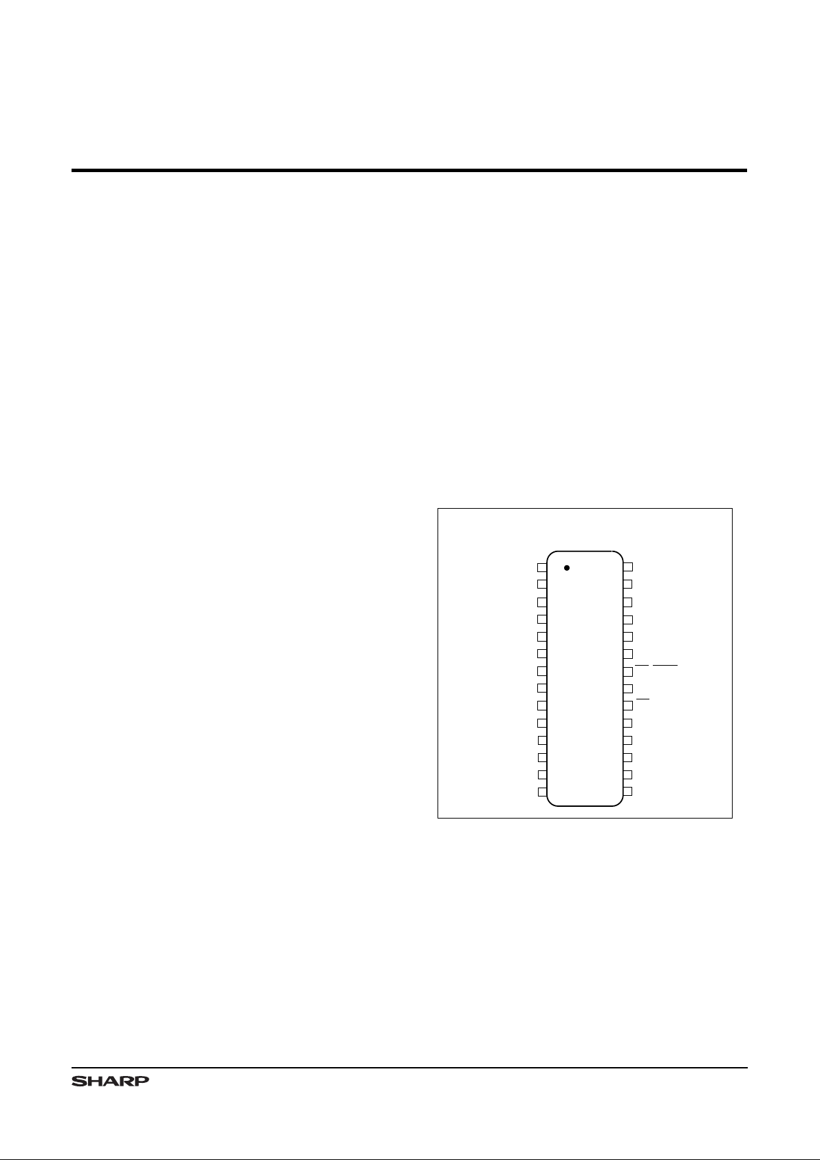
PIN CONNECTIONS
TOP VIEW
1
2
3
4
7
8
A
2
A
5
26
25
24
23
22
21
18
15
A
7
A
6
5
6
A
3
A
4
20
19
A
12
GND
A
8
A
11
A
10
CE
9
10
11
28
27 R/W
A
1
V
CC
12
17
16
A
0
I/O
1
A
9
13
14
OE/RFSH
I/O
2
I/O
3
I/O
7
I/O
6
I/O
5
I/O
4
I/O
8
5P832-1
A
14
A
13
28-PIN DIP
28-PIN SK-DIP
28-PIN SOP
Figure 1. Pin Connections for DI P, SK-DIP,
and SOP Packages
1
Page 2
5P832-2
I/O
1
20
CLOCK
GENERATOR
27
22
CE
R/W
A
3
A
2
A
1
A
12
A
11
A
10
A
9
A
8
A
7
A
6
A
4
A
5
A
13
A
14
COLUMN
ADDRESS
BUFFER
ROW
ADDRESS
BUFFER
REFRESH
ADDRESS
COUNTER
DATA
IN
BUFFER
DATA
OUT
BUFFER
I/O
SELECTOR
COLUMN
DECODER
SENSE
AMPS
MEMORY
ARRAY
256 ROWS
128 COLUMNS
ROW
DECODER
EXT/INT
ADDRESS
MUX
I/O
2
I/O
3
I/O
4
I/O
5
I/O
6
I/O
7
I/O
8
V
BB
BIAS-GENERATOR
GND
V
CC
OE/
RFSH
16
17
18
19
15
13
12
11
2
23
21
24
26
1
4
7
8
3
6
25
5
9
28
14
A
0
10
SELF-REFRESH
TIMER
AUTO-REFRESH
CONTROLLER
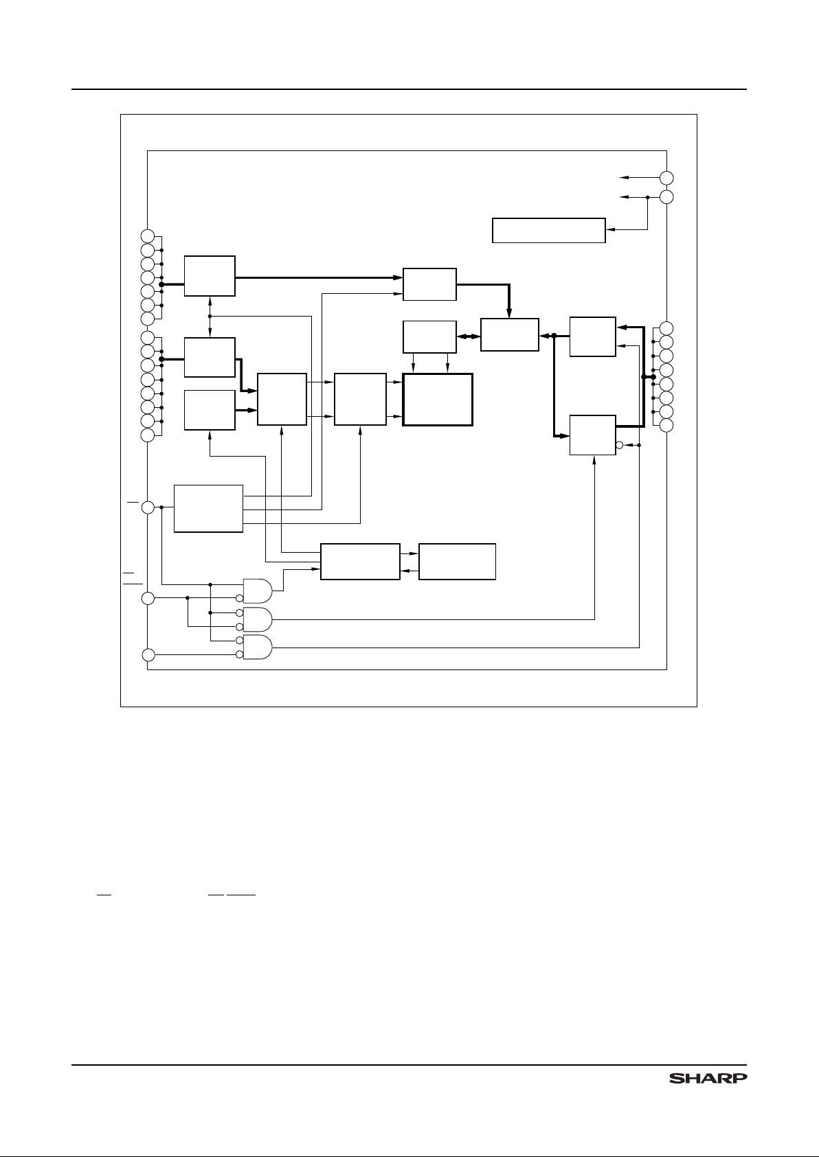
Figure 2. LH5P832 Block Diagram
PIN DESCRIPTION
SIGNA L PIN N AME
R/W Read/ Writ e in put
OE/RFSH Outpu t E nab le/ Ref res h in put
I/O
1
- I/O
8
Data inp uts and outpu ts
A
0
- A
7
Row a ddr ess in put s
SIGNAL PIN NAME
A8 - A
14
Column Add res s inp uts
CE Chip E nab le inp ut
V
CC
Power sup ply
GND Ground
TRUTH TABLE
CE R/W OE/RFSH MODE I/O1 - I/O
8
I
CC
NOTE
L L X Write Data in Operating (I
CC1
)1
L H L Read Data out Operating (I
CC1
)
LHH
CE-Only Refresh High-Z Operating (I
CC1
)
H X L Auto Refresh High-Z Operating (I
CC1
) 1, 2
H X L Self Refresh High-Z Self Refresh (I
CC3
) 1, 3
H X H Standby High-Z Standby (I
CC2
)1
NOTES:
1.
X = H or L 2.
OE Pulsewidth < 8 µs 3. OE Pulsewidth ≥ 8 µs
LH5P832 CMOS 256K (32K × 8) Pseudo-Static RAM
2
Page 3

ABSOLUTE MAXIMUM RATINGS
PARAMETER SYMBOL RATI NG UNIT NOTE
Appli ed v ol tage on an y p in V
T
-1.0 to +7.0 V 1
Output sh ort ci rcu it c urr ent I
O
50 mA
Power dis sipati on P
D
600 mW
Operat ing te mpe ratu re
Topr 0 to +70 °C
Storage temperature Tstg -55 to +150
°C
NOTE:
1. Referenced to GN D
RECOMMENDED OPERATI NG CONDITIONS (TA = 0 to +70°C)
PARAMETER SYMBOL MIN. TYP. MAX. UNIT
Suppl y v olt age V
CC
4.5 5.0 5.5 V
Input vol tage
V
IH
2.4 VCC + 0.3 V
V
IL
-1.0 +0.8 V
CAPACITANCE (VCC = 5.0 V ±10%, TA = 0 t o +70°C, f = 1 MHz)
PARAMETER CONDITIONS SYMBOL MIN. MAX. UNIT
Input cap acitan ce
A
0
- A14, R/W C
IN1
8pF
CE, OE/RFSH C
IN2
5pF
Input/ out put ca pac ita nce
I/O
1
- I/O
8
C
OUT1
12 pF
DC CHARACTERISTICS (VCC = 5 V ± 10%, TA = 0 t o +70°C)
PARAMETER SYMBOL CONDITIONS MIN. MAX. UNIT NOTE
Operat ing cu rre nt I
CC1
tRC = 160 ns 65 mA 1, 2
Operat ing cu rre nt I
CC1
tRC = 190 ns 55 mA 1, 2
Standb y c urr ent I
CC2
CE = VIH, OE/RFSH = V
IH
3mA1
Self r efr esh av era ge c urr ent I
CC3
CE = VIH, OE/RFSH = V
IL
3mA1
CPU in ter nal cy cle
averag e c urr ent
I
CC4
tRC = 160 ns 65 mA 1, 2
CPU in ter nal cy cle
averag e c urr ent
I
CC4
tRC = 190 ns 55 mA 1, 2
Input lea kag e c urr ent I
LI
0 V ≤ VIN ≤ 6 .5 V -10 10 µA
Output le aka ge cur ren t I
LO
0 V ≤ V
OUT
≤ VCC + 0.3 V -10 10 µA3
Output Hi gh vol tag e V
OH
I
OUT
= -1 mA 2.4 V
Output Lo w v olt age V
OL
I
OUT
= 4 mA 0.4 V
NOTES:
1. Specified values are with outputs open.
2. I
CC1
and I
CC4
depend on the cycle time.
3. The output pins are in high-impedance state.
AC TEST CONDITIONS
PARAMETER MODE NOTE
Input voltage amplitude 0.6 to 2.4 V
Input rise/fall time 5 ns
Timing re fer enc e l eve l 1.5 V
Output load conditions 1TTL gate, C
L
= 100 pF 1
NOTE:
1. In cludes scope and jig capacitance.
CMOS 256K (32K × 8) Pseudo-Stat ic R AM LH5P 832
3
Page 4

AC CHARACTERISTICS
READ AND WRITE CYCLES
1,2
(VCC = 5.0 V ±10%, TA = 0 to 70°C)
PARAMETER SYMBOL
160 ns 190 ns
UNIT NOTE
MIN. MAX. MIN. MAX.
Rand om read , w rit e c ycl e t ime t
RC
160 190 ns
Read mo dif y wr ite cy cle ti me t
RMW
225 280 ns
CE p uls e w idt h t
CE
100 10,000 120 10,000 ns
CE p rec har ge t ime t
P
50 60 ns
Addr ess se tup ti me t
AS
00ns
Addr ess ho ld time t
AH
20 30 ns
Read co mma nd h ol d ti me t
RCH
00ns
Read co mma nd s et up t ime t
RCS
00ns
CE a cce ss tim e t
CE A
100 120 ns 3
OE a cce ss tim e t
OEA
40 50 ns 3
CE t o o utpu t i n L ow- Z t
CLZ
10 10 ns
OE to output in Low-Z t
OLZ
00ns
Outp ut e na ble fro m e nd o f w rit e t
WLZ
00ns
Chip di sab le to o utp ut in Hig h-Z t
CHZ
0 30 0 35 ns 2
Outp ut d is abl e to ou tpu t i n H igh -Z t
OHZ
0 30 0 35 ns 2
Write ena ble to ou tpu t in Hi gh- Z t
WHZ
0 30 0 35 ns 2
OE s etu p ti me t
OES
10 10 ns
OE h old tim e t
OEH
00ns
OE lead time t
OEL
10 10 ns
Write com man d p uls e w idt h t
WCP
60 85 ns
Write com man d s etu p t ime t
WCS
60 85 ns
Write com man d h old ti me t
WCH
60 85 ns
Data se tup tim e f rom wri te t
DSW
40 50 ns
Data se tup tim e f rom
CE
t
DSC
40 50 ns
Data ho ld t ime fr om w rit e
t
DHW
00ns
Data ho ld t ime fr om CE
t
DHC
00ns
Transi tion time (ris e and fall)
t
T
335335ns
Refr esh tim e i nte rva l
t
REF
44ms
REFRESH CYCLE
Auto re fres h c yc le t ime t
FC
160 190 ns
Refr esh de lay tim e f rom
CE t
RFD
50 60 ns
Refr esh pu lse wi dth (Au to ref res h) t
FAP
60 8,000 80 8,000 ns
Refr esh pre ch arge ti me
(Aut o re fre sh)
t
FP
30 30 ns
CE d ela y t ime fro m re fre sh act ive
(Aut o re fre sh)
t
FCE
190 225 ns
Refr esh pu lse wi dth (Se lf ref res h) t
FAS
8,000 8,000 ns
CE d ela y t ime fro m re fre sh
prec har ge ( Sel f r efr esh )
t
FRS
190 225 ns
NOTES:
1.
At least 200 µs of pause time after power on should be given for
proper device operation.
CE and OE/RFSH must be fixed at VIH for 2 0 0 µs fr om the V
DD
reached to the specified voltage level
and follo wed by at least 8 dummy cycles.
2. AC character istics are measured at tT = 5 ns.
3. Measured with a load circuit equivalent to 1TTL loads and
100 pF.
LH5P832 CMOS 256K (32K × 8) Pseudo-Static RAM
4
Page 5

t
CE
ADDRESS
DATA
OUT
t
AS
t
AH
t
OEL
t
OES
t
OEH
t
RCS
t
CHZ
t
OEA
5P832-3
t
P
t
RC
t
RCH
t
CEA
t
OHZ
t
OLZ
t
CLZ
CE
A0 - A
14
I/O1 - I/O
8
OE/
RFSH
R/W
V
IH
V
IL
V
IH
V
IL
V
IH
V
IL
V
IH
V
IL
V
OH
V
OL
Figure 3. Read Cycle
t
CE
ADDRESS
t
AS
t
AH
t
WCH
t
OEH
t
OES
t
WCP
5P832-4
t
P
t
RC
t
WCS
CE
A0 - A
14
I/O1 - I/O
8
OE/
RFSH
R/W
V
IH
V
IL
V
IH
V
IL
V
IH
V
IL
V
IH
V
IL
DATA - IN
t
DSW
t
DSC
t
DHW
t
DHC
V
IH
V
IL
Figure 4. Write Cycle
CMOS 256K (32K × 8) Pseudo-Stat ic R AM LH5P 832
5
Page 6

t
CE
ADDRESS
t
AS
t
AH
t
OES
t
OEH
t
WCP
5P832-5
t
P
t
RMW
t
WCS
CE
A0 - A
14
OE/
RFSH
R/W
V
IH
V
IL
V
IH
V
IL
V
IH
V
IL
V
IH
V
IL
DATA - IN
t
DSW
t
DSC
t
DHW
t
DHC
V
IH
V
IL
t
RCS
t
CHZ
V
OH
V
OL
t
CEA
t
OEA
t
OLZ
t
OHZ
t
WHZ
t
WLZ
t
CLZ
DATA OUT
I/O1 - I/O
8
Figure 5. Read/Write Cycle
t
CE
ADDRESS
t
AS
t
AH
t
OEH
t
OES
5P832-6
t
P
t
RC
CE
A0 - A
7
I/O1 - I/O
8
OE/
RFSH
R/W
V
IH
V
IL
V
IH
V
IL
V
IH
V
IL
V
IH
V
IL
V
OH
V
OL
t
RCS
t
RCH
HIGH-Z
NOTE: A8 - A14 = Don't Care
Figure 6. CE Only Refresh Cycle
LH5P832 CMOS 256K (32K × 8) Pseudo-Static RAM
6
Page 7

I/O1 - I/O
8
OE/
RFSH
CE
V
IH
V
IL
V
IH
V
IL
V
OH
V
OL
t
RFD
HIGH-Z
t
FC
t
FAP
t
FP
t
FCE
t
FAP
5P832-7
NOTE: A0 - A14, R/W = Don't Care
Fig ure 7. Auto Refresh Cycl e
I/O1 - I/O
8
OE/
RFSH
CE
V
IH
V
IL
V
IH
V
IL
HIGH-Z
t
RFD
t
FAS
t
FRS
5P832-8
NOTE: A0 - A14, R/W = Don't Care
V
OH
V
OL
Figure 8. Self Refresh Cycle
CMOS 256K (32K × 8) Pseudo-Stat ic R AM LH5P 832
7
Page 8

DIMENSIONS IN MM [INCHES]
MAXIMUM LIMIT
MINIMUM LIMIT
28DIP (DIP028-P-0600)
114
1528
28DIP-2
13.45 [0.530]
12.95 [0.510]
0.51 [0.020] MIN.
5.20 [0.205]
5.00 [0.197]
3.50 [0.138]
3.00 [0.118]
2.54 [0.100]
TYP.
0.60 [0.024]
0.40 [0.016]
0.30 [0.012]
0.20 [0.008]
DETAIL
36.30 [1.429]
35.70 [1.406]
0° TO 15°
4.50 [0.177]
4.00 [0.157]
15.24 [0.600]
TYP.
28-Pin, 600-mil DIP
28SK-DIP (DIP028-P-0300)
DIMENSIONS IN MM [INCHES]
MAXIMUM LIMIT
MINIMUM LIMIT
114
1528
28DIP-1
7.05 [0.278]
6.65 [0.262]
0.51 [0.020] MIN.
4.40 [0.173]
4.00 [0.157]
3.40 [0.134]
3.00 [0.118]
2.54 [0.100]
TYP.
0.56 [0.022]
0.36 [0.014]
0.35 [0.014]
0.15 [0.006]
DETAIL
35.00 [1.378]
34.40 [1.354]
0° TO 15°
3.65 [0.144]
3.25 [0.128]
7.62 [0.300]
TYP.
28-Pin, 300-mil SK-DIP
PACKAGE DIAGRAMS
LH5P832 CMOS 256K (32K × 8) Pseudo-Static RAM
8
Page 9

DIMENSIONS IN MM [INCHES]
MAXIMUM LIMIT
MINIMUM LIMIT
28SOP (SOP028-P-0450)
12.40 [0.488]
11.60 [0.457]
8.80 [0.346]
8.40 [0.331]
10.60 [0.417]
18.20 [0.717]
17.80 [0.701]
0.15 [0.006]
1.025 [0.040]
0.20 [0.008]
0.00 [0.000]
1.025 [0.040]
2.40 [0.094]
2.00 [0.079]
0.20 [0.008]
0.10 [0.004]
0.50 [0.020]
0.30 [0.012]
1.27 [0.050]
TYP.
28 15
141
1.70 [0.067]
1.70 [0.067]
28SOP
28-Pin, 450-mil SOP
10 100
12 120
LH5P832
Device Type
X
Package
- ##
Speed
5P832-9
CMOS 256K (32K x 8) Pseudo Static RAM
Blank 28-pin, 600-mil DIP (DIP028-P-0600)
D 28-pin, 300-mil SKDIP (SKDIP028-P-0300)
N 28-pin, 450-mil SOP (SOP028-P-0450)
Example: LH5P832N-12 (CMOS 256K (32K x 8) Pseudo Static RAM, 120 ns, 28-pin, 450-mil SOP)
Access Time (ns)
ORDERING INFORMATION
CMOS 256K (32K × 8) Pseudo-Stat ic R AM LH5P 832
9
 Loading...