

Page 1
LH5P1632
CMO S 512 K (32 K × 16) Pseudo-Static RAM
FEATURES
•• 32,768 × 16 bi t orga niza tio n
•• Access time: 80/15 0 n s (MAX.)
•• Cycle ti me: 140/210 ns ( MIN.)
•• Sing le +5 V powe r su ppl y
•• Powe r consu mption (MAX.):
Operating : 467.5/327 .5 mW
Standb y: 16.5 mW
•• TTL compatible I/O
•• 256 refresh cycles /4 ms (MAX.)
•• Available for auto-refresh mode
•• Packages:
40-pi n , 600 -mil DIP
40-pi n , 525 -mil S OP
DESCRIPTION
The LH5P1632 is a 512K-bit Pseudo-Static RAM
organized as 32,768 × 16 bits. It is fabricated using
silicon-gate CMOS process technology.
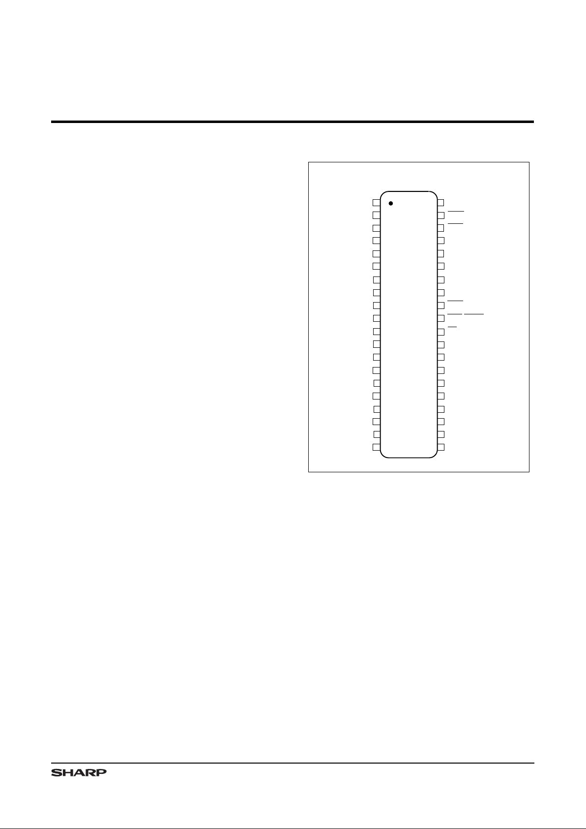
PIN CONNECTIONS
5P1632-1
TOP VIEW
5
6
7
8
11
12
I/O
1
A
2
34
33
32
31
30
29
26
A
4
A
3
9
10
A
0
A
1
28
27
A
5
A
13
A
14
LOE/RFSH
13
14
15
36
35
I/O
2
A
11
I/O
4
UOE/TEST
1
CE
A
6
I/O
13
I/O
14
A
12
40-PIN DIP
40-PIN SOP
3
4
A
7
38
37
LWR
A
8
A
10
1
2
40
39
V
CC
GND
UWR
I/O
3
I/O
15
I/O
16
24
25
16
17
I/O
6
I/O
11
I/O
12
I/O
5
22
23
18
19
I/O
8
I/O
9
I/O
10
I/O
7
21
20 V
CC
GND
A
9
Figure 1. Pin Connections for DIP and
SOP Packages
1
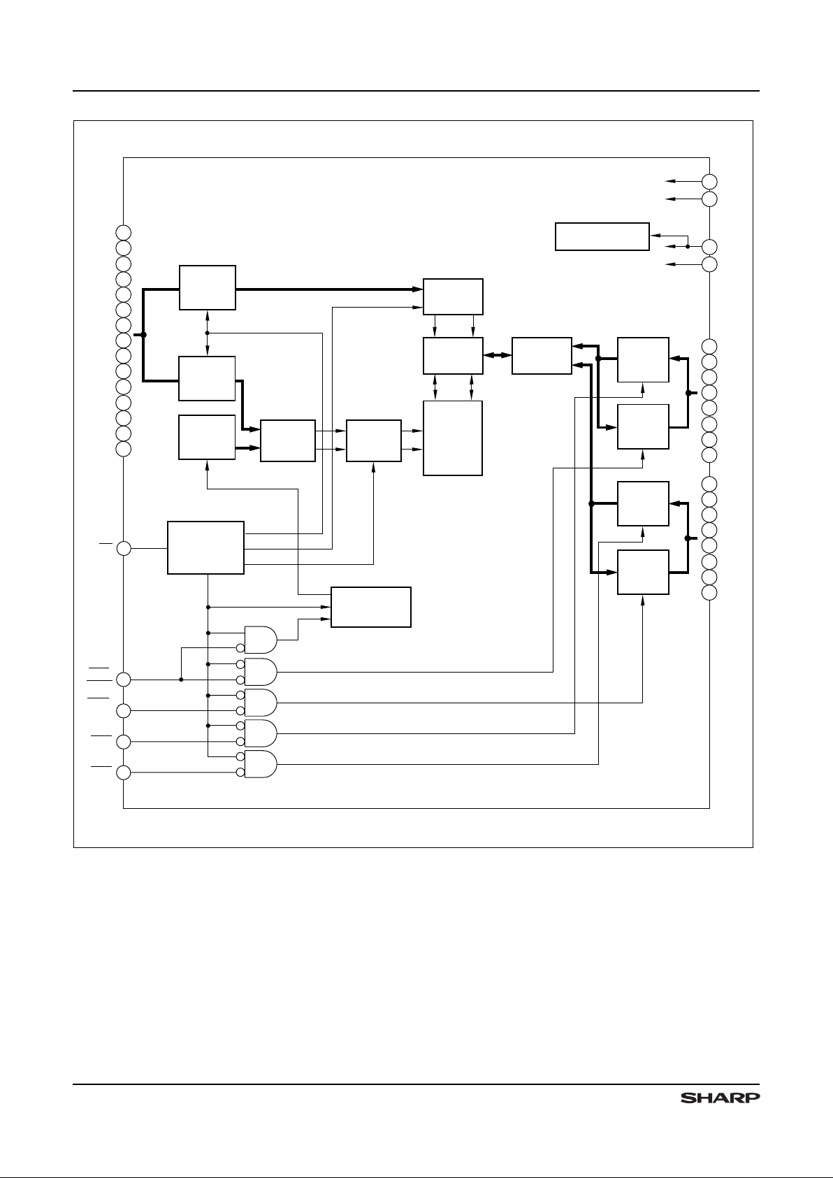
Page 2
I/O
2
CLOCK
GENERATOR
LWR
A
12
A
13
A
14
A
3
A
4
A
5
A
6
A
7
A
8
A
9
A
11
A
10
A
2
A
1
A
0
COLUMN
ADDRESS
BUFFER
ROW
ADDRESS
BUFFER
REFRESH
ADDRESS
COUNTER
DATA
IN
BUFFER
DATA
OUT
BUFFER
I/O
SELECTOR
COLUMN
DECODER
SENSE
AMPS
ROW
DECODER
EXT/INT
ADDRESS
MUX
REFRESH
CONTROLLER
I/O
3
I/O
4
I/O
5
I/O
6
I/O
7
I/O
8
V
BB
GENERATOR
GND
5P1632-2
I/O
1
LOE/
RFSH
UOE/
TEST
1
11
10
9
8
7
6
5
4
3
2
37
36
35
34
33
32
38
21
20
12
13
14
15
16
17
18
19
30
CE
MEMORY
ARRAY
A8 - A
14
A0 - A
7
31
LWR
39
DATA
IN
BUFFER
DATA
OUT
BUFFER
40
1
I/O
10
I/O
11
I/O
12
I/O
13
I/O
14
I/O
15
I/O
16
I/O
9
22
23
24
25
26
27
28
29
V
CC
GND
V
CC
Figure 2. LH5P1632 Block Diagram
PIN DESCRIPTION
SIGNAL PI N N AM E
A0 – A
14
Addre ss input
LWR, UWR Write e na ble
LOE/RFSH, UOE Outpu t e nab le/ Ref res h in pu t
CE Chip ena ble in put
SI GNA L PIN NA ME
I/O1 – I/O
16
Data in put /out put
V
CC
Powe r S upp ly
GND Grou nd
LH5P1632 CMOS 512K (32K × 16) Pseudo-Static RAM
2
Page 3

ABSOLUTE MAXIMUM RATINGS
PARAMETER SYMBOL RATING UNIT NOTE
Appli ed v ol tage on al l p ins V
T
–1.0 to +7.0 V 1
Output sh ort ci rcu it c urr ent I
O
50 mA
Power dis sipati on P
D
600 mW
Operating temperature Topr 0 to +70
°C
Storage temperature Tstg –65 to +150
°C
NOTE:
1. The maximum applicable voltage on any pin with respect to GND.
RECOMMENDED OPERATING CON DITIONS (TA = 0 to +70°C)
PARAMETER SYMBOL M IN. TY P. MAX. UNIT NOTE
Suppl y v olt age
V
CC
4.5 5.0 5.5 V
GND 0 0 0 V
Input vol tage
V
IH
2.4 VCC + 0.3 V
V
IL
–0.3 0.8 V 1
NOTE:
1. VIL (MIN.) = –1. 0 V when the p ulse width is less than 2 0 ns.
CAPACITANCE (TA = 0 to +70°C, f = 1 MHz, VCC = 5.0 V ±10%)
PARAMETER CONDITIONS SYMBOL MIN. MAX. UNIT
Input cap acitan ce
A
0
– A
14
C
IN1
8pF
LWR, UWR C
IN2
5pF
CE
C
IN3
5pF
LOE/RF SH, UOE C
IN4
5pF
Input/ Out put ca pac ita nce I/O
1
– I/O
16
C
OUT1
10 pF
DC CHARACTERISTICS (TA = 0 to +70°C, VCC = 5.0 V ±10%)
PARAMETER SYMBOL CONDITIONS MIN. MAX. U NIT NOTE
Average su ppl y c urr ent in
normal op era tio n
t
RC
= tRC (MIN)
I
CC1
LH5P 163 2-8 0 85
mA 1, 2
LH5P1632-15 65
Suppl y c urre nt in
standb y m ode
I
CC2
3.0 mA 1, 3
Average su ppl y c urr ent in
CPU in ter nal cy cle
(
LWR = UWR = LOE/RFSH =
UOE = VIH)
I
CC3
LH5P 163 2-8 0 85
mA 1, 2
LH5P1632-15
Input lea kag e c urr ent I
LI
0 V ≤ VIN ≤ 6.5 V,
0 V except on tes t pins
–10 10
µA
I/O le aka ge cur ren t
I
LO
0 V ≤ V
OUT
≤ VCC + 0 .3 V,
Outpu ts in high-i mpedan ce
state
–10 10 µA
Output HI GH vol tag e V
OH
I
OUT
= – 1.0 mA 2.4 V
Output LO W v olt age V
OL
I
OUT
= 4 .0 mA 0.4 V
NOTES:
1. Specified values are w ith outputs open.
2. I
CC1
and I
CC3
depend on the cycle time.
3.
CE = H igh, LOE/RFSH = High.
CMOS 512K (32K × 16) Pseudo-Static RAM LH5P1632
3
Page 4

AC CHARACTERISTICS
1, 2, 3
(TA = 0 to +70°C, VCC = 5.0 V ±10%)
PARAMETER SYMBOL
–80 ns –150 ns
UNIT NOTE
MIN. MAX. MIN. MAX.
READ OR WRITE CYCLE
Random re ad, wri te cyc le tim e t
RC
140 210 ns
Read m odi fy wri te c yc le time t
RMW
205 280 ns
CE pul se wid th t
CE
80 10,000 150 10,000 ns
CE pre cha rge ti me t
P
50 60 ns
Addres s s etu p t ime t
AS
0 0 ns 4
Addres s h old ti me t
AH
20 30 ns 4
Read c omm and se tup ti me t
RCS
00ns
Read c omm and ho ld time t
RCH
00ns
CE acc es s t ime t
CEA
80 150 ns 5
OE acces s time t
OEA
30 70 ns 5
CE to out put in Low -Z t
CLZ
10 10 ns
OE to out put in Low -Z t
OLZ
00ns
OE setup tim e for WR t
OS W
00ns
Output di sab le tim e fr om CE
t
CHZ
025035ns
Output di sab le tim e fr om OE t
OHZ
025035ns
Output di sab le tim e fr om
WR t
WHZ
025035ns
OE setup tim e t
OES
10 10 ns
OE hold time t
OEH
00ns
OE lead time t
OEL
10 10 ns
Write c omma nd pul se wid th t
WCP
60 85 ns
Write c omma nd set up tim e t
WCS
60 85 ns
Write c omma nd hol d t ime
t
WCH
60 85 ns
Data s etu p t ime fro m WR t
DSW
30 50 ns
Data s etu p t ime fro m
CE t
DSC
30 50 ns
Data h old ti me f rom
WR t
DHW
00ns
Data h old ti me f rom CE
t
DHC
00ns
Transiti on time (r ise an d fa ll) t
T
335335ns
Refres h t ime in terv al t
RE F
44ms
REFRESH CYCLE
Auto r efr esh cy cle ti me t
FC
140 190 ns
Refres h d ela y t ime fro m
CE t
RFD
50 60 ns
Refres h p uls e w idt h ( Aut o Re fre sh) t
FAP
30 8,000 80 8,000 ns
Refres h p rec har ge time (A uto
Refres h)
t
FP
40 30 ns
CE del ay tim e f rom Ref res h a cti ve
(Auto Ref resh)
t
FCE
160 225 ns
NOTES:
1. I n order to initialize the circuit, CE and OEL/RFSH should be kept
VIH for 200 µs after power on and followed by at least 8 dummy
cycles.
2. AC characteristics shall be tested with t
T
= 5 ns.
3. AC charac teristic s are measured at the following condition (see fi gure
at right).
4. Address is latched at the negative edge of
CE.
5. M easured with a load equivalent to 2TTL + 100 pF.
6. Data f or the lo wer byte (I/O
1
to I /O8) is latched at the positive edge
of
LWR or the positive edge of CE. Data for the upper byte (I/O9 to
I/O
16
) is latched at the positive edge of UWR or the positive edge
of CE.
2.4 V
0.8 V
2.6 V
0.6 V
2.2 V
0.8 V
OUTPUT
INPUT
5P1632-9
Figure 3. AC Characteristics
LH5P1632 CMOS 512K (32K × 16) Pseudo-Static RAM
4
Page 5

TRUTH TABLE
INPUT OUTPUT M ODE
NOTE
CE UOE LOE/RFSH UWR LWR I/O9 – I/O
16
I/O1 – I/O
8
UPPER BYTE LOWER BYTE
H D D D D High-Z High-Z Standby
LL L H H D
OUT
D
OUT
Read Read
L H L H H High-Z D
OUT
CE only refresh Read
LL H H H D
OUT
High-Z Read CE only refresh
L H H H H High-Z High-Z
CE only refresh CE only refresh
LD D L L D
IN
D
IN
Write Write
LD H L H D
IN
High-Z Write CE only refresh
L H D H L High-Z D
IN
CE only refresh Write
LD L L H D
IN
D
OUT
Write Read Inhibit
LL D H L D
OUT
D
IN
Read Write Inhibit
H D D D High-Z High-Z Auto Refresh
NOTES:
D = Don’t care.
High-Z = H igh impedance.
5P1632-3
t
OHZ
VALID-DATA
OUTPUT
V
IH
V
IL
CE
t
P
t
RC
t
CE
t
P
t
AS
ADDRESS
INPUT
t
AH
V
IH
V
IL
A0 - A
14
V
IH
V
IL
t
OEH
t
OEL
t
OES
V
IH
V
IL
LWR
UWR
t
RCS
t
RCH
t
CEA
t
CHZ
t
OEA
t
OLZ
t
CLZ
V
OH
V
OL
I/O1 - I/O
16
LOE/RFSH
UOE
Figure 4. Read Cycle
CMOS 512K (32K × 16) Pseudo-Static RAM LH5P1632
5
Page 6

5P1632-4
t
DSC
VALID-DATA
INPUT
V
IH
V
IL
CE
t
P
t
RC
t
CE
t
P
t
AS
ADDRESS
INPUT
t
AH
V
IH
V
IL
A0 - A
14
V
IH
V
IL
t
OES
t
OEH
V
IH
V
IL
LWR
UWR
t
DSW
t
DHW
V
IH
V
IL
I/O1 - I/O
16
LOE/RFSH
UOE
t
WCH
t
WCS
t
WCP
t
DHC
Figure 5. Write Cycle
LH5P1632 CMOS 512K (32K × 16) Pseudo-Static RAM
6
Page 7

5P1632-5
t
DSC
VALID-DATA
INPUT
V
IH
V
IL
CE
t
P
t
RMW
t
P
t
AS
ADDRESS
INPUT
t
AH
V
IH
V
IL
A0 - A
14
V
IH
V
IL
t
OEH
V
IH
V
IL
LWR
UWR
t
DSW
t
DHW
V
IH
V
IL
LOE/RFSH
UOE
t
RCS
t
WCP
t
DHC
t
OSW
t
WCS
t
WHZ
VALID-DATA
OUTPUT
t
OHZ
V
OH
V
OL
I/O1 - I/O
16
t
CEA
t
OEA
t
OLZ
t
CLZ
Figure 6. Read-Write Cycle
CMOS 512K (32K × 16) Pseudo-Static RAM LH5P1632
7
Page 8

5P1632-6
V
IH
V
IL
CE
t
P
t
RC
t
CE
t
P
t
AS
ADDRESS
INPUT
t
AH
V
IH
V
IL
A0 - A
7
V
IH
V
IL
t
OES
LOE/RFSH
UOE
V
IH
V
IL
LWR
UWR
V
OH
V
OL
I/O1 - I/O
16
t
OEH
t
RCS
t
RCH
HIGH - Z
NOTE: A
8
- A
14
= Don't Care
Figure 7. CE Only Refresh Cycle
5P1632-7
V
IH
V
IL
CE
V
OH
V
OL
I/O1 - I/O
16
t
RFD
t
FCE
HIGH - Z
NOTE: A
0
- A14, LWR, UWR, UOE = Don't Care
t
FAP
V
IH
V
IL
LOE/RFSH
t
FC
t
FP
t
FAP
Fig ure 8. Auto Refresh Cycle
LH5P1632 CMOS 512K (32K × 16) Pseudo-Static RAM
8
Page 9

13.45 [0.530]
12.95 [0.510]
0.51 [0.020] MIN.
5.40 [0.213]
4.80 [0.189]
3.55 [0.140]
2.95 [0.116]
2.54 [0.100]
TYP.
0.60 [0.024]
0.40 [0.016]
0.30 [0.012]
0.20 [0.008]
DETAIL
DIMENSIONS IN MM [INCHES]
52.30 [2.059]
51.70 [2.035]
0° TO 15°
MAXIMUM LIMIT
MINIMUM LIMIT
4.55 [0.179]
3.95 [0.156]
15.24 [0.600]
TYP.
40DIP (DIP040-P-0600)
120
2140
40DIP
40-pin, 600-mil DIP
DIMENSIONS IN MM [INCHES]
MAXIMUM LIMIT
MINIMUM LIMIT
40SOP (SOP040-P-0525)
14.50 [0.571]
13.70 [0.539]
11.50 [0.453]
11.10 [0.437]
12.50 [0.492]
26.50 [1.043]
26.10 [1.028]
0.15 [0.006]
1.275 [0.050]
0.20 [0.008]
0.00 [0.000]
1.275 [0.050]
2.90 [0.114]
2.50 [0.098]
0.20 [0.008]
0.10 [0.004]
0.50 [0.020]
0.30 [0.012]
1.27 [0.050]
TYP.
40
21
201
1.40 [0.055]
1.40 [0.055]
40SOP
40-pin, 525-mil SOP
PACKAGE DIAGRAMS
CMOS 512K (32K × 16) Pseudo-Static RAM LH5P1632
9
Page 10

15 150
80 80
LH5P1632
Device Type
X
Package
- ##
Speed
5P1632-8
CMOS 512K (32K x 16) Pseudo-Static RAM
Example: LH5P1632N-80 (CMOS 512K (32K x 16) Pseudo-Static RAM, 80 ns, 40-pin, 525-mil SOP)
D 40-pin, 600-mil DIP (DIP040-P-0600)
N 40-pin, 525-mil SOP (SOP040-P-0525)
Access Time (ns)
ORDERING INFORMATION
LH5P1632 CMOS 512K (32K × 16) Pseudo-Static RAM
10
 Loading...