

Page 1
LH5496/96H
CMOS 512 × 9 FIFO
FEATURES
•• Fast Access Times :
15 */20/25/35/50/65/ 80 ns
•• Full CMOS Dual Port Memor y Arr ay
•• Fully Async hronous Read and Write
•• Expandable-in Width and Depth
•• Full, Half-F ull, and Empty Status Flags
•• Read Retransmit Capability
•• TTL Compatible I/O
•• Packages:
28-Pin, 300-mil PDIP
28-Pin, 600-mil PDIP
32-Pin PLCC
•• Pin an d Fu nct io n all y C omp at ibl e wi th I DT 72 01
FUNCTIONAL DESCRIPTION
The LH5496/ 96H are dual por t memor ies with inter nal
addressing to implement a First-In, First-Out algorithm.
Through an advanc ed dual por t archit ecture, they provide
fully asynchr onous read/wr ite ope ration. Empty, Full, and
Half-Full status flags are provided to prevent data overflow and underflow . In addition, interna l logic provides for
unlimited expansion in bot h word size and depth.
Read and write operations automatically access sequential locat ions in memory in that data is read out in the
same order that it was written, that is on a First-In,
First-O ut basis. Since the addr ess s equen ce is internally
predefined, no external address info rmation is required
for the oper ation of this dev ice. A nint h data bit is pro vided
for parity or contro l inform at ion oft en needed in comm unication applicat ions.
Empty, Full, and Half-Full status flags monitor the
extent to which data has been writt en int o the FIFO, and
prevent improper operations (i.e., Read if the FIFO is
empty, or Write if the FIFO is full). A retransmit feature
resets the Read address pointer to i ts initial position,
thereby allowing repetitive readout of the same data.
Expansion In and Expansion Out pins implement an
expansion scheme that allows individual FIFOs to be
cascaded to greater depth without incurring additional
latency ( bubblet hrough) delays .
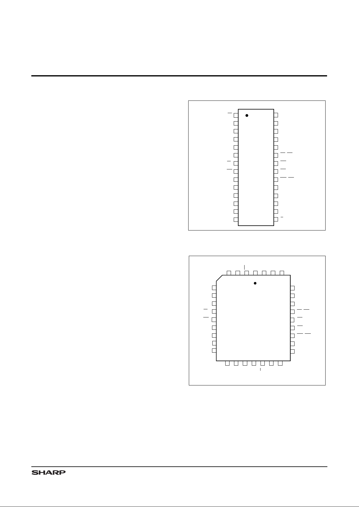
PIN CONNECTIONS
5496-1D
1
2
3
4
5
6
7
8
9
10
11
12
13
14
W
D
8
D
3
D
2
D
1
D
0
XI
FF
Q
0
V
SS
28
27
26
25
24
23
22
21
20
19
18
17
16
15
V
CC
D
4
FL/RT
RS
EF
XO/HF
R
Q
1
Q
2
Q
3
Q
8
D
6
D
5
D
7
Q
7
Q
6
Q
5
Q
4
28-PIN PDIP TOP VIEW
Figur e 1. Pin Connections for PDIP Packages
5
6
7
8
9
10
D
2
D
1
D
0
XI
FF
Q
0
11Q
1
2
3
4
32
31
30
29
28
27
26
25
24
D
6
D
7
NC
EF
D3D
8
W
NC
V
CC
D
4
D
5
14
15
16
20
19
18
17
FL/RT
RS
23
XO/HF
22
Q
7
21
Q
6
12NC
13Q
2
1
Q3Q
8
V
SS
NC
R
Q
4
Q
5
5496-2D
32-PIN PLCC TOP VIEW
Figure 2. Pin Connections for PLCC Package
* LH5496 only.
1
Page 2
PIN DESCRIPTIONS
PIN PIN TYPE * DESCRIPTION
D0 – D
8
I
Input Data Bus
Q0 – Q
8 O/Z
Output Dat a Bu s
W
I
Write Request
R
I
Read Request
EF
O
Empty Flag
FF
O
Full Flag
* I = Input, O = Output, Z = High-Impedance, V = Power Volta ge Level
PIN PIN TYPE * DESCRIPTION
XO/HF
O
Expansion Out/Half-Full Flag
XI
I
Expansion In
FL/RT
I
First Load/ Retransmit
RS
I
Reset
V
CC
V
Positive Power Supply
V
SS
V
Ground
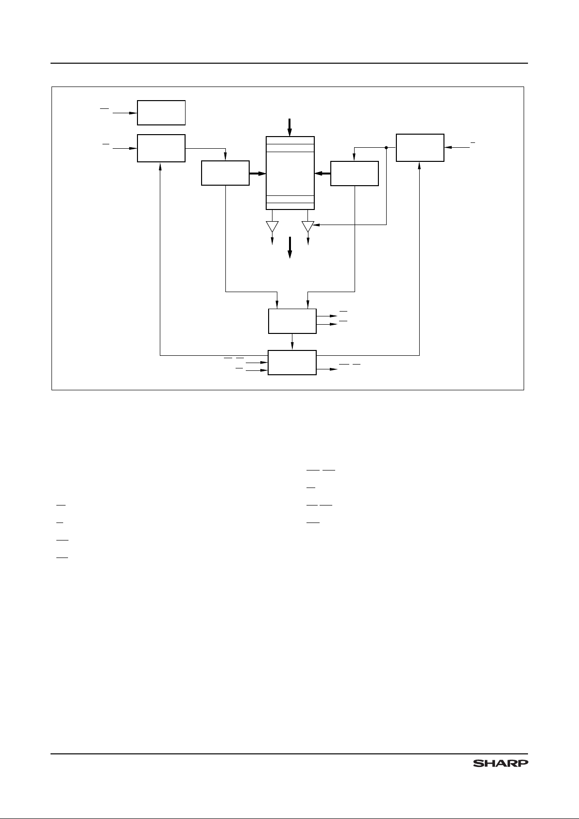
DATA OUTPUTS
Q
0
- Q
8
FLAG
LOGIC
WRITE
POINTER
READ
POINTER
DATA INPUTS
D
0
- D
8
DUAL-PORT
RAM
ARRAY
512 x 9
EF
FF
. . .
5496-3
INPUT
PORT
CONTROL
R
W
RESET
LOGIC
RS
OUTPUT
PORT
CONTROL
EXPANSION
LOGIC
XO/HF
XI
FL/RT
Figure 3. LH5496/96H Block Diagram
LH5496/96H CMOS 512 × 9 FIFO
2
Page 3

ABSOLUTE MAXIMUM RATINGS
1
PARAMETER RATING
Supply Volt age t o VSS Potential –0.5 V to 7 V
Signal Pin Voltage to VSS Potential
3
–0.5 V to VCC + 0.5 V (not to exceed 7 V)
DC Output Current
2
±50 mA
Storage T e mperature Range –65oC to 150oC
Power Dissipation (Package Limit) 1.0 W
DC Voltag e Applied T o Outpu ts In High-Z State –0.5 V to Vcc + 0.5 V (not to exceed 7 V)
NOTES:
1. Stresses greater than those listed under ‘Absolute Maximum Ratings’ may cause permanent damage to the device.
This is a device stress rating for transient conditions only. Functional operatio n at these or any other conditions above
those indicated in the ‘Operating Range’ of this specification is not implied. Exposure to absolute maximum rating
conditi ons for extended periods may affect reliability.
2. Outputs should not be shorted for more than 30 seconds. No more than one output should be shorted at any time.
3. Negative undershoots of 1.5 V in amplitude ar e permitted for up to 10 ns once per cycle.
OPERATING RANGE
SYMBOL PARAMETER MIN MAX UNIT
T
A
T emperat ure, Ambient, LH5496
070
o
C
T
A
T emperature, Ambient, LH5496H
–40 85
o
C
V
CC
Supply Voltage
4.5 5.5 V
V
SS
Supply Voltage
00V
VILLogic ‘0 ’ Input V oltag e
1
–0.5 0.8 V
V
IH
Logic ‘1 ’ Input V oltag e
2.0 VCC + 0.5 V
NOTE:
1. Negative undershoots of 1.5 V in amplitude ar e permitted for up to 10 ns once per cycle.
DC ELECTRICAL C HARACTERISTICS (O ver Operat ing Range)
SYMBOL PARAMETER TEST CO NDITIONS MIN MAX UNIT
I
LI
Inpu t Leakage Cur rent VCC = 5.5 V, VIN = 0 V to V
CC
–10 10
µA
I
LO
Output Leakage Current
R ≥ VIH, 0 V ≤ V
OUT
≤ V
CC
–10 10
µA
V
OH
Output High Voltage IOH = –2.0 mA
2.4 V
V
OL
Output Low Voltage IOL = 8.0 mA
0.4 V
I
CC
Aver age Supply Cur rent
1
Measu red at f = 40 MHz
100 mA
I
CC2
A ver age Sta ndby Cur re nt
1
All Inputs = V
IH
15 mA
I
CC3
Power Down Current
1
All Inputs = VCC – 0.2 V
5mA
NOTE:
1. ICC, I
CC2
, and I
CC3
are dependent upon actual output loading and cycle rates. Specified values are with outputs open.
CMOS 512 × 9 FIFO LH5496/96H
3
Page 4

AC TE ST C O NDI T IO N S
PARAMETER RAT IN G
Input Pulse Levels
VSS to 3 V
Input Rise and Fall Times (10% to 90%)
5 ns
Input Tim ing Ref ere nce Lev els
1.5 V
Output Refer ence Le vels
1.5 V
Output L oad, Timing Test s
Figure 4
CAP ACI TANCE
1,2
PARAMETER RATING
CIN (Input Capacitance)
5 pF
C
OUT
(Output Capacitance)
7 pF
NOTES:
1. Sample tested only.
2. Capacitances are maximum values at 25oC measured at 1.0 MHz
with VIN = 0 V.
5496-4
DEVICE
UNDER
TEST
+5 V
30 pF
1.1 k Ω
680 Ω
INCLUDES JIG & SCOPE CAPACITANCES
*
*
Figure 4. Output Load C ircuit
LH5496/96H CMOS 512 × 9 FIFO
4
Page 5

AC ELECTRICAL CHARACTERISTICS 1 (Over Operat ing Range)
SYMBOL PARAMETER
tA = 15 ns 2tA = 20 ns tA = 25 ns tA = 35 ns tA = 50 ns tA = 65 ns tA = 80 ns
UNIT
MIN MAX MIN MAX MIN MAX MIN MAX MIN MAX MIN
MAX
MIN MAX
READ CYCLE TIMING
t
RC
Read Cycle Time 25 – 30 – 35 – 45 – 65 – 80 – 100 – ns
t
A
Access T im e – 15 – 20 – 25 – 35 – 50 – 65 – 80 ns
t
RR
Read Recover Time 10 – 10 – 10 – 10 – 15 – 15 – 15 – ns
t
RPW
Read Pulse Width
3
15 – 20 – 25 – 35 – 50 – 65 – 80 – ns
t
RLZ
Data Bus Active from Read LOW 45 – 5– 5–5– 5– 5–10– ns
t
WLZ
Data Bus Acti ve fro m Wri te
HIGH
4,5
10 – 10 – 10 – 10 – 10 – 10 – 20 – ns
t
DV
Data Valid from Read Pulse HIGH
5 – 5– 5–5– 5– 5–5 –ns
t
RHZ
Data Bus High-Z from Read
HIGH
4
– 15 – 15 – 15 – 15 – 20 – 30 – 30 ns
WRITE CYCLE TIMING
t
WC
Write Cycle Time 25 – 30 – 35 – 45 – 65 – 80 – 100 – ns
t
WPW
Write Pulse Width
3
15 – 20 – 25 – 35 – 50 – 65 – 80 – ns
t
WR
Write Recovery Time 10 – 10 – 10 – 10 – 15 – 15 – 15 – ns
t
DS
Data Setup Time 10 – 10 – 10 – 15 – 20 – 20 – 20 – ns
t
DH
Data Hold Time 0 – 0 – 0 – 0 – 0 – 5 – 5 – ns
RES ET TIMING
t
RSC
Reset Cycl e Ti me 25 – 30 – 35 – 45 – 65 – 80 – 100 – ns
t
RS
Reset Puls e Width
3
15 – 20 – 25 – 35 – 50 – 65 – 80 – ns
t
RSR
Reset Reco very Ti me 10 – 10 – 10 – 10 – 15 – 15 – 15 – ns
t
RRSS
Read HIGH to RS HIGH 15 – 20 – 25 – 35 – 50 – 65 – 80 – ns
t
WRSS
Write HIGH to RS HIGH 15 – 20 – 25 – 35 – 50 – 65 – 80 – ns
RETRANSMIT TIMING
t
RTC
Retransmit Cycle Time
25 – 30 – 35 – 45 – 65 – 80 – 100 – ns
t
RT
Retransmit Pulse Width
3
15 – 20 – 25 – 35 – 50 – 65 – 80 – ns
t
RTR
Retransmit Recovery Time 10 – 10 – 10 – 10 – 15 – 15 – 15 – ns
FLAG TIMING
t
EFL
Reset LOW to Empt y Flag LOW – 25 – 30 – 35 – 45 – 65 – 80 – 100 ns
t
HFH,FFH
Reset LOW to Half -Fu ll and Full
Flags HIGH
– 25 – 30 – 35 – 45 – 65 – 80 – 100 ns
t
REF
Read LOW to Empty Flag LOW – 20 – 25 – 25 – 35 – 45 – 60 – 60 ns
t
RFF
Read HIGH to Full Flag HIGH – 20 – 25 – 25 – 35 – 45 – 60 – 60 ns
t
WEF
Write HIGH to Empty Flag HIGH – 20 – 25 – 25 – 35 – 45 – 60 – 60 ns
t
WFF
Write LOW to Full Flag LOW – 20 – 25 – 25 – 35 – 45 – 60 – 60 ns
t
WHF
Write LOW to Half-Full Flag LOW
– 25 – 30 – 35 – 45 – 65 – 80 – 100 ns
t
RHF
Read HIGH to Half -Fu ll Flag HIG H – 25 – 30 – 35 – 45 – 65 – 80 – 100 ns
EXPANSION TIMING
t
XOL
Expansion Out LOW – 18 – 20 – 25 – 35 – 50 – 65 – 80 ns
t
XOH
Expansion Out HIGH – 18 – 20 – 25 – 35 – 50 – 65 – 80 ns
t
XI
Expansion In Pulse Width 15 – 20 – 25 – 35 – 50 – 65 – 80 – ns
t
XIR
Expansi on In Reco very Tim e 10 – 10 – 10 – 10 – 10 – 10 – 10 – ns
t
XIS
Expansi on in Setu p Ti me 7 – 10 – 10 – 15 – 15 – 15 – 15 – ns
NOTES :
1. LH5496 only.
2. A ll timing measurements performed at ‘AC Test Condition’ levels.
CMOS 512 × 9 FIFO LH5496/96H
5
Page 6

OPERATIONAL DESCRI PT ION
Reset
The device is reset whenever the Reset pin (RS) is
taken to a LOW state. The rese t operatio n init i alizes both
the read and write address pointers to the firs t memory
location. The XI and FL pins are also sam pled at this time
to determine whether the device is in Single mode or
Depth Expansion mode. A reset pulse is required when
the device is first powered up. The Read (R) and Write
(W) pins may be in any sta te when reset is initia ted , but
must be brought to a H IGH state t
RPW
and t
WPW
before
the rising edge of RS. The reset operati on forces the
Empty Flag EF to be asserted (EF = LOW), and the
Half-Full F lag HF and the Full FLag FF to be deasserted
(HF = FF = HIGH); t he Data Out pins (D0 – D8) are forced
into a high-impedanc e state.
Wri te
A write cycle is initiated on the falling edge of the Write
(W) pin. Data setu p and h old times must be obs erved on
the data i n (D0 – D8) pins. A write op eration is only possible
if the FIFO is not full, (i.e. the Full flag pin is HIGH). Wr ites
may occur independently of any ongoing read opertations.
At the falling edge of the first write after the memor y is
half filled, the Half-Full flag will be asserted (HF = L OW)
and will remain asserted u ntil the dif f ere nce be tween the
write point er and read p ointer indicates that the rema ining
data in the device is less than or equal to one half the tot al
capacity of the FIFO. The Half-Full flag is deasserted
(HF = HIGH) by the appropria te rising edge of R.
The Full flag is as serted (FF = LOW) at the falling edge
of the write operation wh ich fills the last available location
in the FIFO memory array . The Full flag will inhibit further
writes until cleared by a valid read. The Full flag is
deasserted (FF = HIGH) after the next rising edge of R
rele ases ano the r memo ry location.
Read
A r ead cycle is initiat ed o n the fa lling edg e of th e Read
(R) pin. Read data becomes valid on the data out (Q0–Q8)
pins after a time tA from the falling edge of R. After R goes
HIGH, the data out pins return to a high-im pedance state.
Reads may occur independent of any ongoing write
operations. A read is only possible if the FIFO is not empty
(EF = HIGH).
The in ternal read a nd write address p ointers are m aintained by the device such that consecutive read operations w ill access data in the same order as it was writ ten.
The Empty f lag is asserted (EF = L OW ) after the f al ling
edge of R which accesses the last available data in the
FIFO memory. EF is deasserted (EF = HIGH ) afte r the
next rising edge of W loads another word of valid data.
Data Flow-Through
Read flow-through mode occurs when the Read (R)
pin is brought LOW whil e the FI FO is empty, a nd held
LOW in anticip ation of a write cycle. At the end of the nex t
write cycle, the Empty flag will be momentarily deasser ted , and the d at a just writ ten will become av ailabl e on
the data out pins after a maximum time of t
WEF
+ tA.
Additiona l writes may occur while the R pin re mains LO W ,
but only data from the first write flows through to the
out puts. Additional data, if any , can only be accessed by
toggling R.
Write flow-through mode occurs when the Write (W)
pin is brough t LOW while the FIFO is full, and held LOW
in anticipat ion of a read cycle. At t he end of the r ead cyc le,
the Full flag will be mo mentarily deasserted, but then
imm ediately reass erted in r esponse to W h eld LOW. Data
is written into the FIFO on the rising ed ge of W which may
occur t
RFF
+ t
WPW
after the read.
Retransmit
The FI FO c an b e made to r eread previously rea d dat a
thr ough the retransmit funct ion. Retransmit is init iate d by
pulsing RT LOW. This resets the internal read address
pointer to the first physical location in the memory while
leaving the internal write address pointer unchanged.
Data between the read and write pointers may be reaccessed by subsequent reads. Both R and W must be
inactive (HIGH) during the retransmi t pulse. Retransmit
is useful if no more than 512 writes are performed between r es ets. Ret ransm it may af fect the st atus o f EF, HF,
and FF fl ags, depending on the relocation of the read
point er. This function is not available in depth expansion
mode.
LH5496/96H CMOS 512 × 9 FIFO
6
Page 7

TIMING DIAGRAMS
t
RS
EFL
t
RSR
t
RRSS
t
WRSS
t
FFHtHFH
t
,
RS
R,W
EF
FF,HF
5496-14
NOTES:
1. t
RSC
= tRS + t
RSR
.
2. W and R ≥ V
IH
around the rising edge of RS.
3. The Data Out pins (D
0
- D8) are forced into a
high-impedance state whenever EF = LOW.
t
RSC
Figure 5. Reset Timi ng
W
t
WPW
t
RLZ
t
A
t
WC
t
A
t
RPW
t
DV
t
RHZ
VALID DATA OUT
t
RR
R
t
RC
t
WR
t
DH
t
DS
5496-5
Q0 - Q
8
D0 - D
8
VALID DATA OUT
VALID DATA IN VALID DATA IN
Figure 6. Asynchron ous Write and Read Oper atio n
CMOS 512 × 9 FIFO LH5496/96H
7
Page 8

FF
R
t
RFF
t
WFF
LAST WRITE FIRST READ
W
5496-6
Figure 7. Full Flag from Last Write to First Read
EF
W
R
t
WEF
t
REF
LAST READ FIRST WRITE
5496-7
NOTE: The Data Out pins (D0 - D8) are forced into a
high-impedance state whenever EF = LOW.
Figure 8. Empty Flag from Last Read to First Write
TIMING DIAGRAMS (co nt ’d)
LH5496/96H CMOS 512 × 9 FIFO
8
Page 9

TIMING DIAGRAMS (co nt ’d)
RPE
t
WEF
t
REF
t
WLZ
t
A
t
5496-8
W
R
EF
D0 - D
8
Q0 - Q
8
VALID DATA OUT
VALID DATA IN
NOTES:
1. t
RPE
= t
RPW
2. t
RPE
: Effective Read Pulse Width after Empty Flag HIGH.
3. The Data Out pins (D
0
- D8) are forced into a
high-impedance state whenever EF = LOW.
Figur e 9. Read Data Flow-Through
WPF
t
R
W
FF
t
WFF
t
RFF
t
DH
t
DS
t
A
D0 - D
8
Q0 - Q
8
5496-9
NOTES:
1. t
WPF
= t
WPW
2. t
WPF
: Effective Write Pulse Width after Full Flag HIGH.
VALID DATA OUT
VALID DATA IN
Figur e 10. Write Data Flow-Throu gh
CMOS 512 × 9 FIFO LH5496/96H
9
Page 10

TIMING DIAGRAMS (co nt ’d)
t
WEF
W
t
RPE
EF
R
5496-10
NOTES:
1. t
RPE
= t
RPW
2. t
RPE
: Effective Read Pulse Width after Empty Flag HIGH.
3. The Data Out pins (D
0
- D8) are forced into a
high-impedance state whenever EF = LOW.
Figur e 1 1. Empty Flag Tim ing
R
FF
W
5496-11
NOTES:
1. t
WPF
= t
WPW
2. t
WPF
: Effective Write Pulse Width after Full Flag HIGH.
t
RFF
t
WPF
Figure 12. Full Flag Timing
HF
W
R
t
RHF
t
WHF
5496-12
HALF-FULL
OR LESS
MORE THAN
HALF-FULL
HALF-FULL
OR LESS
LH5496/96H CMOS 512 × 9 FIFO
10
Page 11

TIMING DIAGRAMS (co nt ’d)
5496-13
NOTES:
1. t
RTC
= t
RT
+ t
RTR
2. EF, HF and FF may change state during retransmit, but flags will be valid at t
RTC
.
RT
t
RTR
t
RT
R,W
Figure 14. Retransmit Timing
t
XOL
t
XOH
READ FROM
LAST VALID
LOCATION
t
XOH
t
XOL
XO
5496-15
WRITE TO LAST
AVAILABLE
LOCATION
W
R
Figure 15. Expansion Out Timing
t
XIS
R
5496-16
XI
W
WRITE TO FIRST
AVAILABLE
LOCATION
t
XIS
READ FROM FIRST
VALID
LOCATION
t
XIR
t
XI
Figure 16. Expansion In Timing
CMOS 512 × 9 FIFO LH5496/96H
11
Page 12

OPERATIONAL MO DES
Single Device Configuration
When depth expansion is not required for the given
application, the device is placed in Single mode by tying
the Expansion In pin (XI) to ground. This pin is intern a lly
sampled during res et.
Width Expansion
Word- width expansion is implemente d by placing multiple L H5496/96H devices in parallel. Each LH5496/96H
should be configured for standalone mode . In this arrang ement, the behavior of the stat us flags is identical for
all devices; so, in principle, a represen tative value for
each o f these f lags could be derived f rom any on e device.
In practice, it is b etter to derive ‘composite’ flag values
using ext ernal logic, since there may be minor speed
var iations between dif f er ent actual devices. (See Figures
17 and 18. )
WRITE
DATA IN
D
0
- D
8
9
FULL FLAG
RESET
XI
RT
RETRANSMIT
EMPTY FLAG
9
READ
HF
LH5496/96H
W
FF
RS
R
EF
DATA OUT
Q
0
- Q
8
5496-17
Figure 17. Single FIF O (512 × 9)
DATA IN
18
WRITE
FULL FLAG
RESET
9
READ
EMPTY FLAG
R
EF
XI
RT
R
W
5496-18
RS
RETRANSMIT
RT
XI
HF
W
FF
RS
9
18
DATA OUT
9
HF
9
LH5496/96H
LH5496/96H
Figure 18. FIFO Width Ex pansi on (512 × 18)
LH5496/96H CMOS 512 × 9 FIFO
12
Page 13

OPERATIONAL MO DES (cont’d )
Depth Expansion
Depth expansion is implemente d by configuring the
required number of F IFOs in Expansion mode. In this
arrangem ent, the FIFOs are conne cted in a circular fashion with the Expansion Out pin (XO) of each device tied
to the Expansion In pin (XI ) of the next device. One FIFO
in this group must be designated as the firs t load device.
This is accomplished by tying the First Load pin (FL) of
this device to ground. All other devices must have their
FL pin tied to a high level. In this mode, W and R signals
are shar ed by all devices, while internal logic contro ls the
steering of data. Only one FIFO will be enabled for any
given read cycle, s o the common Data Out pins of all
devices are wire-ORed together. Likewise, the common
Data In pins of all devices are tied together .
In Expansion mode, external logic is required to generate a comp osit e Full or Empty flag . This is achieved by
ORin g th e FF pins of all devices and ORing the EF pins
of all devices respectively. The Half-Full flag and
Retransmit functions are not available in Depth Expansion mode.
5496-19
RS
RS
FF
9
9
RS
W
FF
DATA IN
D
0
- D
8
RS
FF
9
9
9
R
9
DATA OUT
Q
0
- Q8
FL
FL
EF
XI
XO
FL
EF
Vcc
Vcc
XO
XO
9
9
XI
XI
EMPTY
FULL
EF
LH5496/96H
LH5496/96H
LH5496/96H
Fig ur e 19. FIFO Depth Expan sion (1536 × 9)
CMOS 512 × 9 FIFO LH5496/96H
13
Page 14

OPERATIONAL MO DES (cont’d )
Compound Expansion
A combination o f width and depth expansion can be
easily implemented by operating groups of depth
expanded FI FOs in parallel.
Bidirectional Operation
Applications which require bidirect ional data buffering
between two systems can be realized by operating
LH5496/96H devices in parallel but opposite directions.
The Data In pins of a device may be tied to the corresponding Data O ut pins of anot her d evice o per ating in the
opposit e direct ion to for m a single bidirect ional bus inter face. Care must be taken to assure that the appropriate
read, write , and flag signals are routed to each system.
Both depth and width expansion may be used in this
configuration.
LH5496/96H
DEPTH EXPANSION
BLOCK
LH5496/96H
DEPTH EXPANSION
BLOCK
LH5496/96H
DEPTH EXPANSION
BLOCK
Q
0
- Q
8
DATA OUT
D
N-9
- D
N-1
D18 - D
N-1
D9 - D
N-1
D0 - D
N-1
DATA IN
R
W
RS
Q0 - Q
N-1
Q0 - Q
17
5496-20
Q0 - Q
N-10
Figure 20. Compound FIFO Expansi on
LH5496/96H
LH5496/96H
SYSTEM A SYSTEM B
Qb0 - 8
Db0 - 8
Da0 - 8
Qa0 - 8
XI
Wb
Ra
EFa
HFa
RTa
RS
FFb
RTb
HFb
EFb
Rb
5496-21
XI
Wa
FFa
RS
Figur e 21. Bidirect i onal FIFO Buffer
LH5496/96H CMOS 512 × 9 FIFO
14
Page 15

PACKAGE DIAGRAMS
28SK-DIP (DIP028-P-0300)
DIMENSIONS IN MM [INCHES]
MAXIMUM LIMIT
MINIMUM LIMIT
114
1528
28DIP-1
7.05 [0.278]
6.65 [0.262]
0.51 [0.020] MIN.
4.40 [0.173]
4.00 [0.157]
3.40 [0.134]
3.00 [0.118]
2.54 [0.100]
TYP.
0.56 [0.022]
0.36 [0.014]
0.35 [0.014]
0.15 [0.006]
DETAIL
35.00 [1.378]
34.40 [1.354]
0° TO 15°
3.65 [0.144]
3.25 [0.128]
7.62 [0.300]
TYP.
28-pin, 300-mil PDI P
DIMENSIONS IN MM [INCHES]
MAXIMUM LIMIT
MINIMUM LIMIT
28DIP (DIP028-P-0600)
114
1528
28DIP-2
13.45 [0.530]
12.95 [0.510]
0.51 [0.020] MIN.
5.20 [0.205]
5.00 [0.197]
3.50 [0.138]
3.00 [0.118]
2.54 [0.100]
TYP.
0.60 [0.024]
0.40 [0.016]
0.30 [0.012]
0.20 [0.008]
DETAIL
36.30 [1.429]
35.70 [1.406]
0° TO 15°
4.50 [0.177]
4.00 [0.157]
15.24 [0.600]
TYP.
28-pin, 600-mi l PDIP
CMOS 512 × 9 FIFO LH5496/96H
15
Page 16

ORDERING INFO RMATION
1.27 [0.050]
4 SIDES BSC
14.05 [0.553]
13.89 [0.547]
15.11 [0.595]
14.86 [0.585]
11.51 [0.453]
11.35 [0.447]
12.57 [0.495]
12.32 [0.485]
3.56 [0.140]
3.12 [0.123]
2.41 [0.095]
1.52 [0.060]
0.81 [0.032]
0.66 [0.026]
0.53 [0.021]
0.33 [0.013]
32PLCC
MAXIMUM LIMIT
MINIMUM LIMIT
DIMENSIONS IN MM (INCHES)
0.38 [0.015]
MIN
DETAIL
10.92 [0.430]
9.91 [0.390]
13.46 [0.530]
12.45 [0.490]
0.10 [0.004]
32PLCC (PLCC32-P-R450)
32-pi n, 450-mil PLCC
15
*
20
25
35
50
65
80
Blank 28-pin, 600-mil Plastic DIP (DIP28-P-600)
D 28-pin, 300-mil Plastic DIP (DIP28-P-300)
U 32-pin Plastic Leaded Chip Carrier (PLCC32-P-R450)
LH5496/96H
Device Type
X
Package
- ##
Speed
CMOS 1K x 9 FIFO
Access Time (ns)
X
Temperature
Range
Blank Commercial (0° C to 70° C)
H Industrial (-40° C to 85° C)
5496MD
Example: LH5496U-25 (CMOS 512 x 9 FIFO, 32-pin PLCC, 25 ns)
*
LH5496 only
LH5496/96H CMOS 512 × 9 FIFO
16
 Loading...