

Datasheet LH543621P-20, LH543621P-15, LH543621M-30, LH543621M-25, LH543621M-15 Datasheet (Sharp)
...Page 1

LH543611/2 1
FEATURES
••
Pin-Compatible and Functionally
Upwards-Com pat ible w ith Sharp LH5420 and
LH543601, but Deeper
••
Expanded Control Regi ster that is Fully
Readable as well as Wr itea bl e
••
Fast Cycle Times: 18/20/25/30/35 ns
••
Impro ved In put Set up and Fla g Out Timi ng
••
Two 512 × 36-bit FIFO Buffers (LH543611) or
Two 1024 × 36-bit FIFO Buffers (LH543 621)
••
Full 36-bit Word Width
••
Selectable 36/ 18/9- bit Word Width on Port B;
Selection May be Changed Without Resetti ng
the BiFIFO
••
Programmabl e Byte-Ord er Rever sal –
‘Big-Endi an ↔ Little -Endian Conversion’
••
Independ ently-Syn chr onized (‘Fully-Asynchr onou s’)
Operation of Port A and Port B
••
‘Synchr onou s’ Enab le-Plus- C lock Contro l at
Both Ports
••
R/W , Enab le, Reque st, and Ad dress Cont r ol Inp uts
are Sampled on t he Rising Clock Edge
••
Synchrono us Request /Ack nowledge ‘Handshake’
Capability; Use is Optional
••
Device Comes Up Into a Known Default State at
Reset; Progr am ming is Allowed, but is not Required
••
Asynchron ous O utput Enables
••
Five Status F lags per Port: Full, Almost-Full,
Half-Full, Alm ost-Empt y , and Empt y
••
All Fla gs are Indepen dent ly Program ma ble for
Either Synchronous or Asynchronous O peration
••
Almost-Full Flag and Almost -Empt y Flag Have
Programm able Of fsets
••
Mailbox Registers with Synchronized Flags
••
Data-Bypa ss Function
••
Data -Ret ra nsmit Function
••
Automatic Byte Parit y Checking with
Program mabl e Pari t y Flag L atc h
••
Programmabl e Byte Parity Generat ion
••
Programm abl e Byte, Half- W ord, or Full-W or d
Orient ed Pari t y Operat i on s
••
8 mA-IOL High-Drive Three-State Outputs with
Buil t-In Series Resist or
••
TTL/CMO S-Compat ible I/O
••
Space-Saving PQ FP and TQFP P ac kages
FUNCTIONAL DESCRIP TIO N
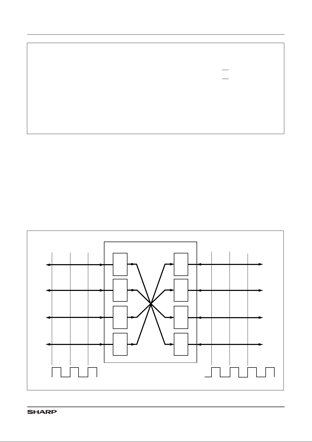
The LH543611 and LH543621 contain t wo FIFO buff ers, FIFO # 1 and FIFO #2 . These operate in parallel, bu t
in opposite directions, for bidirectional data buffering.
FIFO #1 and FIFO #2 each are organize d as 512 or 1024
by 36 bits. The LH54361 1 and LH543621 ar e ideal eith er
for wide unidirectional applications or for bi directional
data appl ications; component count and board area are
reduce d.
The LH543611 and LH543621 have two 36-bit ports,
Port A and Port B. Each port has its own port-synchronous clock, but the two ports may operate asynchronously relative to each other . Data flow is in itiat ed at a port
by the r ising edge of the appropr iat e clock; it is gat ed by
the correspondi ng edge-s ampled enable, request, and
read/write control signals. At the maximum operating
frequency, the clock duty cycle may vary fro m 40% to
60%. At lower frequenci es, the clock waveform may be
quite asymmetric, as long as the minimum pulse-width
conditions for clock-HIGH and clock-LOW remain satisfied; the LH54361 1 and LH543621 are fully-static part s.
Conceptuall y, the por t clocks CKA and CKB are freerunning, periodic ‘clock’ wavefor ms, used to control other
signals which are edg e-sensit ive. Howeve r, th ere actually
is not any absolute requirement that these ‘clock’ waveforms must be periodic. An ‘asynchr onous’ mode of operation is possible, in one or both directions,
independently, if the appropriate enable and request inputs are continuously asserted, and enough aperiodic
‘clock’ pulses of suit able duration are gener ated by external logic to cause all necessar y actions to occur.
A synchronous request/acknowledge handshake
facility is provided at each port for FIFO data access. This
reques t/ ac knowledge handshake resolves FI FO f ul l and
empty boundary co nditions, when the two ports are operated asyn chr onous ly relative to each other.
FIFO status flags monitor the extent to which each
FIFO buffer has been filled. Full, Almost-Full, H alf-Full,
Almost-Empty, and Empty flags are included for
each
FIFO. Each of these flags may be independently program med for e ither synch ronous o r async hronous operation. Al so, t he Almost -Full and Almost-Emp ty fl ags are
programmable over the entire FIFO depth, but are automatic al ly initializ ed to eight locations f rom the respect i ve
FIFO boundar ies at reset . A data block of 512 (LH54361 1)
or 1024 (LH543621 ) or fewer words may be retransmitted
any desired number of times.
512 × 36 × 2 / 1024 × 36 × 2
Synchronous Bidirectional FIFO
BOLD = Additions over the 5420/3601 feature set
1
Page 2

Two mailbox registers provide a separate path for
passing control words or status words between ports.
Each mailbox has a New-Mail -Alert Flag, which is synchronized to th e reading port’s clock. This mailbox function facilitates the synchronization of data transfers
between asyn chronous systems.
Data-bypass mode allows Port A to direc tly transf er
data to or from Port B at reset. In this mode, the device
acts as a registered transceiver under the control of
Port A. For instance, a master processor on Port A can
use the data bypass fea tur e to send or receive initialization or configuration information directly, to or from a
perip her al device on Por t B, during sy st em start up.
A word-width-select option i s p rovided on Port B for
36-bit, 18-bit, or 9-bit data access. This fea ture allows
word-width matching between Port A and Port B, with no
additional logic nee ded. It also ensu res maximum util ization of bu s band widths. Sub ject to meeting tim ing requirements, the word-width selection may be changed at any
time during the operation of an LH543611 or LH543621,
without the n eed either for a res et o peration or for pa ssing
dummy words through Port B immediately after the
change; except that if the change is not made at a
full-word boundary, at least one du mmy word must be
passed through Port B before any actual data words
are transmitted.
A Byte Parity Check Flag at each port monitors data
integrity. Control-Register bit 00 (zero) selects the parity
mode, odd or even. This bit is init ialized for odd data parity
at reset; but it may b e r eprogrammed for even parity, or
back again to odd par ity , as desired. The parity flags may
be program med to oper ate eithe r in a latched mode or in
a flowthrough mode. The parity checking may be performed over 36-bit full-words, over 18-bit half-words, or
over 9-b it single byt es.
Parity generation may be selected as well as parity
checking, and may likewise be performed over full-words
or half-words or si ngle bytes. In any case, a parity bit of
the proper mode is genera ted over the least-significant
eight bits of a byt e, and then is st ored in the m ost- significant bit position of the byte as it passes through the
LH543611/21, overwriting whatever bit was present in
that bit position previously.
LH543611/21 512 x 36 x 2/ 1024 x 36 x 2 BiFIFOs
2
Page 3
116
115
114
113
112
111
110
109
108
107
106
105
104
103
102
101
100
99
98
97
96
95
94
93
92
91
90
89
88
87
86
85
84
18
19
20
21
22
23
24
25
26
27
28
29
30
31
32
33
34
35
36
37
38
39
40
41
42
43
44
45
46
47
48
V
CCO
D
10A
D
9A
D
8A
V
SSO
D
7A
D
6A
D
5A
D
4A
D
3A
D
2A
D
1A
D
0A
RS
RT
1
D
1B
D
2B
D
3B
D
4B
D
5B
D
6B
D
7B
D
8B
D
9B
D
10B
D
11B
V
CCO
V
SSO
V
SSO
V
CCO
V
SSO
V
CCO
49
50
D
0B
515253545556575859606162636465666768697071727374757677787980818283
V
CCO
D
24A
D
25A
D
26A
V
SSO
D
27A
D
28A
D
29A
D
30A
D
31A
D
32A
D
33A
D
34A
D
35A
RT
2
D
35B
D
34B
D
33B
D
32B
D
31B
D
30B
D
29B
D
28B
D
27B
D
26B
D
25B
V
CCO
V
SSO
V
SS
V
SSO
V
CCO
V
SSO
V
CCO
17
16151413121110
9876543
2
Pin 1
Pin 132
131
130
129
128
127
126
125
124
123
122
121
120
119
118
117
D
12AD13AD14A
V
SSO
D
15AD16AD17A
HF1AF1FF1OE
A
A2AA
1A
A
0A
R/WAENAVSSACKAEF2MBF2D
18A
D
19A
D
20AD21AD22A
V
CC
CKAREQ
A
AE
2
V
SSO
D
23
A
D
11A
D
12BD13BD14B
V
SSO
D
15B
D
16BD17B
AE
1
EF
1
REQ
B
EN
B
R/W
B
CK
B
WS
0
WS
1
V
CC
FF
2
AF
2
PF
B
D
18B
D
19B
D
20B
D
21B
D
22B
V
SS
A
0B
HF
2
V
SSO
D
23
B
MBF
1
ACK
B
OE
B
D
24
B
PF
A
543611-1
TOP VIEW
CHAMFERED
EDGE
132-PIN PQFP
Figur e 1. Pin Connect ions for 132-Pi n PQF P Pa ckage
(Top View)
PIN CONNECTIONS
512 x 36 x 2/ 1024 x 36 x 2 BiFI FOs L H543611/21
3
Page 4
108
107
106
105
104
103
102
101
100
99
98
97
96
95
94
93
92
91
90
89
88
87
86
85
84
83
82
81
80
79
78
77
76
1
2
3
4
5
6
7
8
9
10
11
12
13
14
15
16
17
18
19
20
21
22
23
24
25
26
27
28
29
30
31
D
24A
D
25A
D
27A
D
28A
D
30A
D
31A
D
33A
D
34B
D
33B
D
31B
D
30B
D
28B
D
27B
32
33
RT
2
128
127
V
CCO
D
10A
D
9A
V
SSO
D
7A
D
6A
V
CCO
D
4A
D
3A
V
SSO
D
1A
RS
D
0B
D
2B
V
SSO
D
3B
D
5B
V
CCO
D
6B
D
8B
V
SSO
D
9B
D
5A
D
2A
D
1B
D
4B
D
7B
D
10B
144
143
142
141
140
139
138
137
136
135
134
133
132
131
130
129
126
125
124
123
122
121
120
119
118
117
116
115
114
113
112
D
23AD22AD21A
V
SSO
D
19AD18A
AE2EF2ACKAREQ
A
ENAR/W
A
CK
A
A
0A
OEAVCCFF1HF1PF
A
D
17A
D
15A
V
SSO
D
14A
V
SS
AF
1
D
13A
D
24BD23B
V
SSO
D
22B
D
20B
PF
B
OE
B
WS
1
A
0B
R/W
B
EN
B
REQ
B
ACK
B
EF
1
MBF
1
D
16B
V
SSO
V
SS
D
17B
D
15B
HF
2
CK
B
D
14B
TOP VIEW
MBF
2
543611-2
34
35
36
V
CCO
D
11B
V
CCO
75
74
73
111
110
D
12AD11A
109
53
54
373839404142434445464748495051
52
5556575859606162636465666768697071
72
D
13BD12B
V
CCO
D
26A
V
SSO
D
29A
V
CCO
D
32A
V
SSO
D
34A
D
35A
V
SSO
D
32B
V
CCO
D
29B
V
SSO
D
26B
D
25B
D
21B
D
19BD18B
AF
2
FF
2
V
CC
WS
0
AE
1
D
8A
RT
1
D
0A
D
20A
A1AA
2A
D
16A
D
35B
V
SS
144-PIN TQFP
V
SSO
V
SS
V
SSO
FR
1
V
SSO
V
CCO
V
CCO
V
SSO
V
SSO
V
SS
V
SSO
FR
2
Figure 2. Pin Connecti ons for 144- Pin TQFP Package
(Top View)
LH543611/21 512 x 36 x 2/ 1024 x 36 x 2 BiFIFOs
4
Page 5

PIN LIST
SIGNAL
NAME
PQFP
PIN NO.
TQFP
PIN NO.
A
0A
1 126
A
1A
2 125
A
2A
3 124
OE
A
4 123
FF
1
6 121
AF
1
7 120
HF
1
8 119
PF
A
9 118
D
17A
10 117
D
16A
11 116
D
15A
12 115
D
14A
14 113
D
13A
15 112
D
12A
16 111
D
11A
17 110
D
10A
19 106
D
9A
20 105
D
8A
21 104
D
7A
23 102
D
6A
24 101
D
5A
25 100
D
4A
27 98
D
3A
28 97
D
2A
29 96
D
1A
31 94
D
0A
32 93
RS 33 92
RT
1
34 91
D
0B
35 89
D
1B
36 88
D
2B
37 87
D
3B
39 85
D
4B
40 84
D
5B
41 83
D
6B
43 81
D
7B
44 80
D
8B
45 79
D
9B
47 77
D
10B
48 76
D
11B
49 75
D
12B
51 71
D
13B
52 70
D
14B
53 69
D
15B
54 68
D
16B
56 66
D
17B
57 65
MBF
1
58 64
AE
1
59 63
SIGNAL
NAME
PQFP
PIN NO.
TQFP
PIN N O.
EF
1
60 62
ACK
B
61 61
REQ
B
63 59
EN
B
64 58
R/
W
B
65 57
CK
B
66 56
A
0B
67 55
WS
0
68 53
WS
1
69 52
OE
B
70 51
FF
2
72 49
AF
2
73 48
HF
2
74 47
PF
B
75 46
D
18B
76 45
D
19B
77 44
D
20B
78 43
D
21B
80 41
D
22B
81 40
D
23B
82 39
D
24B
83 38
D
25B
85 34
D
26B
86 33
D
27B
87 32
D
28B
89 30
D
29B
90 29
D
30B
91 28
D
31B
93 26
D
32B
94 25
D
33B
95 24
D
34B
97 22
D
35B
98 21
RT
2
100 18
D
35A
101 17
D
34A
102 16
D
33A
103 15
D
32A
105 13
D
31A
106 12
D
30A
107 11
D
29A
109 9
D
28A
110 8
D
27A
111 7
D
26A
113 5
D
25A
114 4
D
24A
115 3
D
23A
117 143
D
22A
118 142
D
21A
119 141
SIGNAL
NAME
PQFP
PIN122 NO.
TQFP
PIN NO.
D
20A
120 140
D
19A
122 138
D
18A
123 137
MBF
2
124 136
AE
2
125 135
EF
2
126 134
ACK
A
127 133
REQ
A
129 131
EN
A
130 130
R/
W
A
131 129
CK
A
132 128
V
CC
5 122
V
SSO
13 114
V
SSO
109
V
CCO
108
V
CCO
18 107
V
SSO
22 103
V
CCO
26 99
V
SSO
30 95
V
SSO
90
V
SSO
38 86
V
CCO
42 82
V
SSO
46 78
V
CCO
50 74
V
CCO
73
V
SSO
72
V
SSO
55 67
V
SS
62 60
V
SS
54
V
CC
71 50
V
SSO
79 42
V
SSO
37
V
CCO
36
V
CCO
84 35
V
SSO
88 31
V
CCO
92 27
V
SSO
96 23
V
SS
99 20
V
SSO
19
V
SSO
104 14
V
CCO
108 10
V
SSO
112 6
V
CCO
116 2
V
CCO
1
V
SSO
144
V
SSO
121 139
V
SS
128 132
V
SS
127
NOTE:
PINS COMMENTS
V
CC
Supply internal logic. Connected to each other.
V
CCO
Supply output drivers only. Connected to each
other.
PINS COMMENTS
V
SS
Supply int erna l logic . Connec ted to each other .
V
SSO
Supply out put dri vers only. Connected to each
other .
512 x 36 x 2/ 1024 x 36 x 2 BiFI FOs L H543611/21
5
Page 6
RESET
LOGIC
PORT A
I/O
RS
PORT A
SYNCH-
RONOUS
CONTROL
LOGIC
READ
POINTER
WRITE
POINTER
FIXED AND
PROGRAMMABLE
STATUS FLAGS
FIFO #1
MEMORY ARRAY
512 x 36/1024 x 36
MAILBOX
REGISTER
#2
READ
POINTER
WRITE
POINTER
FIFO #2
MEMORY ARRAY
512 x 36/1024 x 36
PORT B
I/O
FF
1
HF
1
AF
1
EF
2
AE
2
EF
1
AE
1
FF
2
HF
2
AF
2
WS0, WS
1
D0A - D
35A
OE
A
ACK
A
REQ
A
EN
A
R/W
A
CK
A
D0B - D
35B
OE
B
RT
1
ACK
B
REQ
B
EN
B
R/W
B
CK
B
COMMAND
PORT AND
REGISTER
A
0B
RESOURCE
REGISTERS
PARITY
CHECKING
AND
GENERATION
A
0A
A
1A
A
2A
RT
2
COMMAND
PORT AND
REGISTER
MAILBOX
REGISTER
#1
BYPASS
MBF
1
MBF
2
PORT B
SYNCH-
RONOUS
CONTROL
LOGIC
FIXED AND
PROGRAMMABLE
STATUS FLAGS
543611-4
PF
A
PF
B
PARITY
CHECKING
AND
GENERATION
FR
1
FR
2
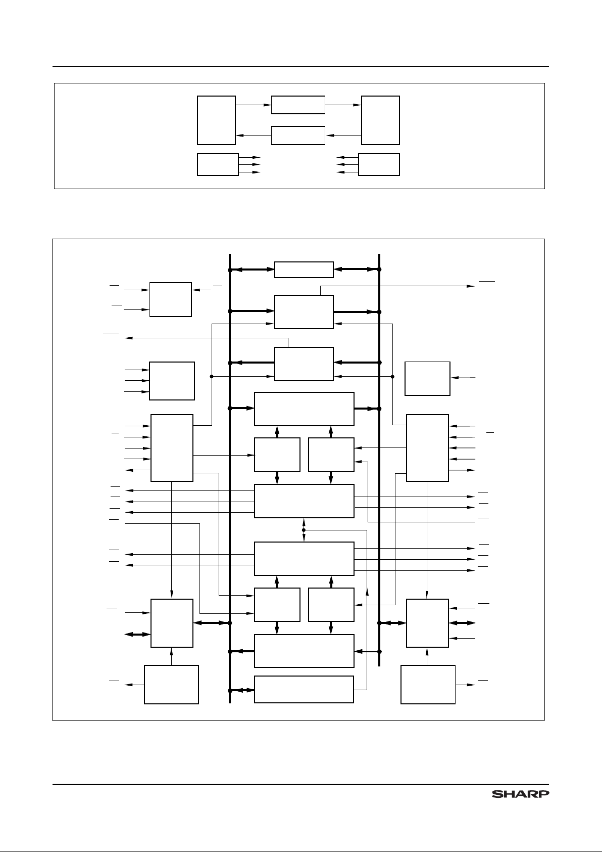
Figur e 3b. Detai led LH54361 1/ 21 Block Diag ram
FIFO 1
PORT A
I/O
FIFO 2
PORT B
I/O
WRITE
READ
WRITE
READ
PORT A
CONTROL
PORT B
CONTROL
543611-3
Figure 3a. Simplified LH54361 1/21 Bloc k Diagram
LH543611/21 512 x 36 x 2/ 1024 x 36 x 2 BiFIFOs
6
Page 7

PIN DESCRIPTIONS
PIN PIN TYPE
1
DESCRIPTION
GENERAL
VCC, V
SS
V
Power, Ground
RS I Reset
PORT A
CK
A
I
Port A Fre e-R unni ng Clo ck
R/
WA
I
Port A Edge -Sam pled Read/ Wr ite Co ntr ol
EN
A
I
Port A Edg e-Sa mple d Enab le
A
0A
, A1A, A
2A
I
Port A Edg e-S ampl ed Ad dres s Pin s
OE
A
I
Port A Leve l-Se nsit ive Ou tput Enabl e
REQ
A
I
Port A Re ques t/En abl e
RT
2
I
FIFO #2 Retr ansm it
D
0A
– D
35A
I/O/Z
Port A Bidi rect iona l Data Bus
FF
1
O
FIFO #1 Full Fla g (Wri te Boun dary )
AF
1
O
FIFO #1 Pro gram mab le Alm ost- Ful l Flag (Writ e Bound ary)
HF
1
O
FIFO #1 Half-Full Flag
AE
2
O
FIFO #2 Prog ram mabl e Almos t-E mpty Flag (Re ad Boun dar y)
EF
2
O FIFO #2 Empty Flag (Read Boundary)
MBF
2
O
New-Mail-Alert Flag for Mailbox #2
PF
A
O
Port A Par ity Fl ag
ACK
A
O
Port A Acknowledg e
PORT B
CK
B
I
Port B Free-Running Clock
R/
W
B
I
Port B Edge-Sampled Read/Write Control
EN
B
I
Port B Edge-Sampled Enable
A
0B
I
Port B Edge-Sampled Address Pin
OE
B
I
Port B Level-Sensitive Output Enable
WS
0
, WS
1
I
Port B Word-Width Select
REQ
B
I
Port B Request/Enable
RT
1
I
FIFO #1 Retr ansm it
D
0B
– D
35B
I/O/Z
Port B Bidirectional Data Bus
FF
2
O
FIFO #2 Full Fla g (Wri te Boun dary )
AF
2
O
FIFO #2 Prog ram mabl e Almos t-F ull Fl ag (W rit e Bound ary)
HF
2
O
FIFO #2 Half-Full Flag
AE
1
O
FIFO #1 Prog ram mabl e Almos t-E mpty Flag (Re ad Boun dar y)
EF
1
O
FIFO #1 Empty Flag (Read Boundary)
MBF
1
O
New-Mail-Alert Flag for Mailbox #1
PF
B
O
Port B Parity Flag
ACK
B
O
Port B Ack nowl edg e
NOTE:
1. I = Input, O = Output, Z = High-Impedance, V = Pow er Voltage Lev el
512 x 36 x 2/ 1024 x 36 x 2 BiFI FOs L H543611/21
7
Page 8

ABSOLUT E MAXIMUM R ATINGS
1
PARAMETER RATING
Supply Volt age t o VSS Potential –0.5 V to 7 V
Signal Pin Volt age t o VSS Potential
3
–0.5 V to VCC + 0.5 V
DC Output Current
2
± 40 mA
Storage Tempera ture Range –65oC to 150oC
Power Dissipation ( Package Limit) 2 Watts (Quad Flat Pack)
NOTES:
1. Stresses greater than those listed under ‘Absolute Maximum Ratings’ may cause permanent damage to the device. This is a stress rating for
transient conditions only. Functional operation of the device at these or any other cond itions out side those indicated in the ‘Operating Rang e’
of this specification is not implied. Exposure t o absolute maximum rating conditions for ex tended periods may affe c t rel iability.
2. Outputs should not be shorted for more than 30 seconds. No more than one output should be shorted at any time.
3. Negative undershoot of 1.5 V in amplitude is permitted for up to 10 ns, once per cycle.
OPERATING RANGE
SYMBOL PARAMETER MIN MAX UNIT
T
A
T emper ature, Ambi ent
070
o
C
Vcc Supply Voltage
4.5 5.5 V
Vss Supply Voltage
00V
V
IL
Logic LOW
Input Voltage
1
–0.5 0.8 V
V
IH
Logic HIGH
Input Voltage
2.2 Vcc + 0.5 V
NOTE:
1. Negative undershoot of 1.5 V in amplitude is permit ted
for up to 10 ns, once per cycle.
DC ELECTRICAL CHARACTERISTI CS (OVER OPERA TING RANGE)
SYMBOL PARAMETER TEST CONDITIONS MIN TYP MAX UNIT
I
LI
Input Leak age Current VCC = 5.5 V, VIN = 0 V To V
CC
–10 – 10 µA
I
LO
I/O Lea kage Cur re nt
OE ≥ VIH, 0 V ≤ V
OUT
≤ V
CC
–10 – 10
µA
V
OL
Logic LOW Output V olt age IOL = 8.0 mA
– – 0.4 V
V
OH
Logic HIG H Output V olta ge IOH = –8.0 mA
2.4 – – V
I
CC
Aver age Supply Cur rent
1, 2
Measur ed at fCC = MAX
– 180 280 mA
I
CC2
A ver age Sta ndby Supply
Curre nt
1, 3
All Input s = V
IHMIN
(Clo cks idle)
–1325mA
I
CC3
Power-Down Supply
Current
1
All Input s = VCC – 0.2 V (Clocks idle)
– 0.002 1 mA
I
CC4
Power-Down Supply
Current
1, 3
All Input s = VCC – 0. 2 V
(Clocks running at fCC = MAX)
–1025mA
NOTES:
1. I
CC
, I
CC 2
, I
CC3
, and I
CC4
are dependent upon actual output loading, and ICC, I
CC4
are also dependent on cycle rates. Specified values are with
outputs op en (for I
CC
: CL = 0 pF); and, for ICC and I
CC4
, operating at minimum cycle times.
2. ICC (MAX.) using VCC = MAX = 5.5 V and ‘worst case’ data pattern. ICC (TYP.) using VCC = 5 V and ‘average’ data pattern.
3. I
CC2
(TYP.) and I
CC4
(TYP.) using VCC = 5 V and TA = 25° C.
LH543611/21 512 x 36 x 2/ 1024 x 36 x 2 BiFIFOs
8
Page 9
AC TEST CONDITIONS
PARAMETER RATING
Input Pulse Levels
VSS to 3 V
Input Rise and Fall T imes
(10% to 90%)
5 ns
Output Re ferenc e Levels
1.5 V
Input Timing Reference Levels
1.5 V
Output Load , Timin g T es ts
Figure 5
CAPACITANCE
1,2
PARAMETER RATING
CIN (Input Capacitance)
8 pF
C
OUT
(Output Capacitanc e)
8 pF
NOTES :
1. Sampl e teste d only.
2. Capacitances are maximum values at 25
o
C, measured at 1.0 MHz, with VIN = 0 V.
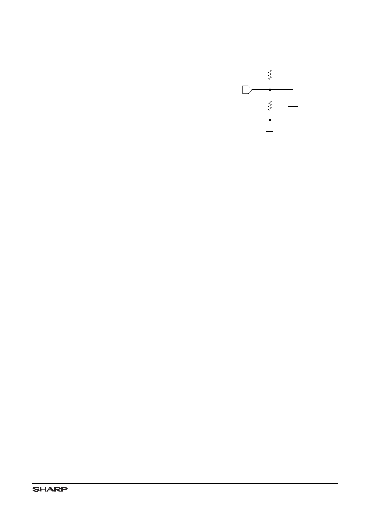
543611-14
+5 V
470 Ω
240 Ω
DEVICE
UNDER
TEST
30 pF
NOTE:
*
= Includes jig and scope capacitances
*
Figure 4. Output Load Cir cui t
512 x 36 x 2/ 1024 x 36 x 2 BiFI FOs L H543611/21
9
Page 10

AC ELECTRICAL CHARACTERISTI CS 1 (VCC = 5 V ± +10%, TA = 0°C to 70°C)
SYMBOL DESCRIPTION
–18 –20 –25 –30 –35
UNITS
MIN MAX MIN MAX MIN MAX MIN MAX MIN MAX
f
CC
Clock Cycle Frequency
—55—50—40—33—28.5MHz
t
CC
Clock Cycle Time
18—20—25—30—35—ns
t
CH
Clock HIGH Time
7—8—10—12—15—ns
t
CL
Clock LOW Time
7—8—10—12—15—ns
t
DS
Data Setup Time
7.5 — 7.5 — 9 — 10 — 12 — ns
t
DH
Data Hold Time
0.5 — 0.5 — 0.5 — 0.5 — 0.5 — ns
t
ES
Enable Setu p T ime
5.5 — 5.5 — 7.5 — 8.5 — 10.5 — ns
t
EH
Enable Hold Ti me
0.5 — 0.5 — 0.5 — 0.5 — 0.5 — ns
t
RWS
Read/Write Setup Time
5.5 — 5.5 — 7.5 — 8.5 — 10.5 — ns
t
RWH
Read/Write Hold Time
0.5 — 0.5 — 0.5 — 0.5 — 0.5 — ns
t
RQS
Request Setup Time
5.5 — 5.5 — 7.5 — 8.5 — 10.5 — ns
t
RQH
Request Hold Time
0.5 — 0.5 — 0.5 — 0.5 — 0.5 — ns
t
AS
Address Set up T ime
2
7.5 — 7.5 — 9 — 10 — 12 — ns
t
AH
Address Hol d Ti me
2
0.5 — 0.5 — 0.5 — 0.5 — 0.5 — ns
t
WSS
Width Select Setup Time
5.5 — 5.5 — 7.5 — 8.5 — 10.5 — ns
t
WSH
Width Select Hold Time
3
0.5 — 0.5 — 0.5 — 0.5 — 0.5 — ns
t
A
Data Outp ut Acc ess T im e
— 13 — 13.8 — 16 — 20 — 25 ns
t
ACK
Acknowle dge A cces s T ime
—9.5—9.5—13—16—18ns
t
OH
Output Hol d Ti me
4—4—4—4—4—ns
t
ZX
Output Ena ble T ime , OE LOW to
D
0
– D35 Low-Z
3
1.5—1.5—2—3—3—ns
t
XZ
Output Dis able Tim e, OE HIGH
to D
0
– D35 High-Z
3
—9—9—12—15—20ns
tEFClock to EF Flag Valid
— 14 — 14.5 — 19 — 22 — 27 ns
t
FF
Clock to FF Flag Valid
— 14 — 14.5 — 19 — 22 — 27 ns
t
HF
Clock to HF Flag Valid
— 14 — 14.5 — 19 — 22 — 27 ns
t
AE
Clock to AE Flag Valid
— 14.5 — 15 — 19 — 22 — 27 ns
t
AF
Clock to AF Flag Valid
— 14.5 — 15 — 19 — 22 — 27 ns
t
MBF
Clock to MBF Flag Valid
—10—10—13—18—23ns
t
PF
Data to Parity Flag Valid
4
—14—14—17—20—25ns
t
RS
Reset/Retransmit Pulse Width
5
18—20—25—30—35—ns
t
RSS
Reset/R etra nsm it Setu p Ti me
6
15—16—20—25—30—ns
t
RSH
Reset/R etra nsm it Hold Tim e
6
7.2— 8 —10—15—20—ns
t
RF
Reset LOW to Flag Valid — 21 — 21 — 25 — 30 — 35 ns
t
FRL
First Read Latency
7
18—20—25—30—35—ns
t
FWL
First Write Latency
8
18—20—25—30—35—ns
t
BS
Bypass Data Setup
8.5—8.5—10—13—15—ns
t
BH
Bypass Data Hold
2—2—3—4—5—ns
t
BA
Bypass Dat a Acc ess
— 15.5 — 16 — 18 — 23 — 28 ns
t
SKEW1
Skew Time Read-to-Write Clock
14 — 14.5 – 19 — 22 — 27 — ns
t
SKEW2
Skew Time Write-to-Read Clock
14 — 14.5 — 19 — 22 — 27 — ns
NOTES:
1. Timing measurements performed at ‘AC Test Condition’ levels.
2. tAS, tAH address setup times and hold t imes need only be satisfied at c lock edges wh ich occur while the correspon d ing enable s are being as-
serted.
3. Values are guaranteed by design; not currently pro duction tested.
4. Measured with Parity Flag operating in f lowthrough mode.
5. Wh en CKA or CKB is enabled; tRS = t
RSS
+ tCH + t
RSH
.
6. t
RSS
and/or t
RSH
need not be met unless a rising edge of C KA occurs while ENA is being asserted, or else a rising edge of CKB occurs while
EN
B
is being asserted.
7. t
FRL
is the minimum first-write-to-first-read delay, following an empty condition, which is required t o assure valid read dat a.
8. t
FWL
is the minimum first-read-to-first-wr ite delay, following a full condition, which is required to assure successful writing of data.
LH543611/21 512 x 36 x 2/ 1024 x 36 x 2 BiFIFOs
10
Page 11

OPERATIONAL DESCRIPTION
Reset
The device is r eset wh enever the asy nchronous Reset
(RS) in put is taken LOW , and at leas t o ne rising edge and
one fal ling edge of both CKA and CKB occur while RS is
LOW . A r eset o perat ion i s req uired after p ower-up, before
the first write operation may occur. The LH543611/21 is
fully ready for operation after being reset. No device
programming is required i f the default states described
below are acceptable .
A reset operation initializes the read-address and
write-address pointers f or FIFO #1 and FIFO #2 to those
FIFO’s f i rst physical memory locations. If the respective
outputs are enabled, the initial contents of these first
locations appea r at the outputs. FIFO and mailbox status
flags are updated to indicate an empty condition. In
addition, the programmable-statu s-flag offset values are
initialized to eight. Thus, the AE1/AE2 flags get asser t ed
within eight locations of an empty condition, and the
AF1/AF2 flags likewise get asserte d wit hin eight locations
of a full condition, for FIFO #1/FIFO #2 respectively.
Bypass Operation
During reset (whenever RS is LOW) the device acts
as a registered transceive r, bypassing the internal FIFO
memories. Port A act s as the mas ter p ort . A write or r ead
operat ion on Port A during reset transf ers dat a directly to
or from Port B. Port B is consider ed to be the slave, and
cannot perform write or read operations independently on
its own during r eset .
The direct ion of the bypass data tr ansmission is deter mined by the R/WA control input, which does not get
overridden by the RS input. Here, a ‘write’ operation
means passing data from Port A to Port B, and a ‘read’
operat ion means p as sing data f rom Por t B to Port A.
The bypass capability may be used to pass initialization or configur ation data direct ly between a master p rocessor and a peripher al device du ring r eset .
Address Modes
Address pins select the device resource to be
accessed by eac h port. Port A has three res our ce- reg ister-select inputs, A0A, A
1A,
and A2A, which se lect between
FIFO access, mailbox-register access, control-register
access, and programmable flag-offset-value-register access. Port B has a single address input, A0B, to select
between FI FO ac cess or mailbox-re gister access.
The status of the resource-register-select inputs is
sampled at t he rising edge of an enabled clock (CKA or
CKB). Resource-r egist er select-input addr ess definitio ns
are summarized in Table 1.
Table 1. Resource- Regis ter Addresses
A2AA1AA
0A
RESOURCE
PORT A
HHH
FIFO
HHL
Mailbox
HLH
AF2, AE2, AF1, AE1 Flag Offsets
Regist er (36- B it Mode)
HLL
Control Register FlagSynchr oniza tion and Par ity
Operating Mode
LHH
AE1 Flag Offset Regist er
LHL
AF1 Flag Offset Register
LLH
AE2 Flag Offset Regist er
LLL
AF2 Flag Offset Register
A
0B
RESOURCE
PORT B
H
FIFO
L
Mailbox
Cont rol Regi st er
The eighteen Control-Register bits govern the synchronization mode of the fullness-status fl ags at each
port, t he choice of odd or even parity at both ports, the
enabl ing o f parity generation for data flow at each port,
the o ptional l atchi ng behavior of the parity -error flags at
each port, and the selection of a full-word o r half-wo rd or
single-byte field for parity checking. A reset operation
initializes the LH543611/21 Control Register for
LH5420/LH 543601-compatible operation, but it may be
reprogrammed at will at any time during LH543611 /21
operation.
FIFO Write
Port A writ es to FIFO #1, a nd Po rt B wr ites to FI FO #2.
A writ e operat ion is initiate d on the rising edge of a clock
(CKA or CKB) whenev er: the appr opr iat e enable (ENA or
ENB) is held HIGH; the appropriate request (REQA or
REQB) is held HIGH; the appr opr iat e Read/ Wr ite contro l
(R/WA or R/WB) is held LOW; the FIFO address is
selected for the a ddress inputs (A2A – A0A or A0B); and
the prescribe d setup times and h old times are observed
for all of these signals. Setup times and hold t im es must
also be observed on the data-bus pins (D0A – D
35A
or
D0B – D
35B
).
Normally, the appropriate Output Enable signal (OE
A
or OEB) is HIGH, to disable the outputs at that port, so
that the data word present on the bus from external
sources gets stored. However, a ‘loopback’ mode of
operation also is possible, in which the data word supplied
by the outputs of one internal FIFO is ‘turned around’ at
the port and read bac k int o the ot her FIFO. In this mode ,
the outputs at the port ar e not disabled. T o rem ain w ithin
specificati on for all timing parameters, the Clock Cycle
Frequency must be reduced slightly below the value
512 x 36 x 2/ 1024 x 36 x 2 BiFI FOs L H543611/21
11
Page 12

which otherwise would be permissible for that speed
grade of LH543611/ 21.
When a FIFO full condition is reached, write operations
are locked out. Following the first read operation from a
full FIFO, another memory location is freed up, and the
corresponding Full Flag is deasserte d (F F = HIGH). The
first write opera tion should begin no earlier than a First
Write Latency (t
FWL
) after the first read operation from a
full FIFO, to ensure that correct read data are retrieved.
(See Figures 33 and 34. )
FIFO Read
Port A reads from FIFO #2, and Port B r eads from FI FO
#1. A read operation is initiated on the rising edge of a
clock (CKA or CKB) wheneve r: the appropriate enable
(ENA or ENB) is held HIGH; the appropriate request
(REQA or REQB) is held HIGH; the appropriate
Read/Write control (R/WA or R/WB) is held HIGH;
the FIFO address is selected for the address inputs
(A2A – A0A or A0B); and the prescribed setup times and
hold times are observed for all of thes e signals. Read data
becomes valid on the data-bus pins (D0A – D
35A
or
D0B – D
35B
) by a time tA after the rising clock (CKA or
CKB) edge, provided that the data outputs are enabled.
OEA and OEB are assertive- LOW, asynchronous , Output Enable con trol input signals. Their effect is onl y t o
enable or disable t he out put drivers of the res pective po rt.
Disabling the output s does
not
dis able a read operation;
data trans mitt ed to the corresp onding out pu t register will
remain available later, when the outputs again are enabled, unless it subsequent ly is overwrit ten .
When an empt y condition is reac hed, read o p erations
are locked out until a valid wr ite operat ion( s) has loaded
additional data into the FI FO. Following the first write to
an empty FIFO, the correspo nding empty flag ( EF) will be
deasser ted ( HI GH) . The first r ead oper ation should begin
no earlier than a First Read Latency (t
FRL
) after the fi rst
write to an empty FIFO, to ensure tha t correct read data
words are retriev ed. (See Figures 31 and 32.)
Dedicated FIFO Status Flags
Six dedicated FIFO status flags are included for Full
(FF1 and FF2), Half-Full ( HF1 and HF2), and Em pty (EF
1
and EF2). FF1, HF1, and EF1 indicate the status of FIFO
#1; and FF2, HF2, an d EF2 indicate the status of FIFO #2.
A Full Flag is asserted f ollowing the first subsequent
rising clock edge for a write operation which fi lls the FIFO.
A Full Flag is deasserted following the first subseque nt
falling clock edge for a read operation to a full FIFO. A
Half-Full Flag i s updat ed following the first subsequent
rising clock edge of a read or write operation to a FIFO
which changes its ‘half-full’ status. An Empty Flag is
asserted following the first subsequent rising clock edge
for a read operation which empties the FIFO. An Empty
Flag is deasserted following the falling clock edge for a
write oper atio n to an empty FIFO.
Programmable Status Flags
Four program mable FIF O statu s flags a re provided,
two for Almost -Full (AF1 and AF2), and two for AlmostEmpt y (AE1 and AE2). Thus, each por t has two p rogrammable flag s to m onit or t he s tatus of the two inte rna l FI FO
buffer memories. The o ffset values for these flags are
initialized to eight locations from the respective FIFO
bounda ries dur ing res et , but can be repr ogr ammed ov er
the entir e FIF O depth.
An Almost-Full Flag is a sser t ed following the first subsequent rising clock edge after a write operation which
has partially filled the FIFO up t o the ‘almost-full’ offset
point . An Almost-F ull Flag is deasserted following the first
subsequent falling clock edge after a read operation
which has partially emptied the FIFO down past the
‘almost-full’ offset point. An Almost-Empty Flag is
asserted following the first subsequ ent rising clock edge
after a read operation which has partially emptied
the FIFO down to the ‘almost-empty’ offset point. An
Almost-Empty Flag i s deasserted following the first subsequent falling clock edge after a write operation which
has partially filled t he FIFO up past the ‘almost-em pt y’
offset point.
Flag of f set s may be wr itt en or r ead thr oug h t he Por t A
dat a bus. All four programm able FIFO status flag off sets
can be set simultaneously through a single 36-bit status
word; or, each programmable flag offset can be set individually , through one of four nine-bit (L H54 361 1) or t en- bit
(LH543621) stat us wor ds. Tables 3a and 3 b illustrat e the
dat a format for flag-pr ogr am ming wor ds. Note that when
all four offsets are set simultaneously i n an LH543621,
the settings a re lim ite d to magn itud es e xpressible in nine
bits; for larger offset values, the individual setting option
mus t be used. (See Figure 3b.)
Also, T ables 4a and 4b define th e meanin g of each of
the five flags, both the dedicate d f lags and the programmable flags, fo r the LH543611 and LH543621 respectively.
NOTE: Cont rol input s wh ich ma y aff ect t he co mpu tation
of flag values at a port generally should not change while
the clock for that port is HIGH, since some updating of
flag values takes place on the
falling
ed ge of t he clock.
Mailb ox Operation
T wo mailbo x registers are provide d for passin g system
hard wa re or softwar e control/status words between por ts.
Each po rt can r ead it s own ma ilbo x and wr ite to the oth er
port’ s m a i lbox. M a i lbox ac cess is performed on t he rising
edge of the controlling FIFO’s clock, with the mailbox
address selected and the enable (ENA or ENB) HIGH.
That is, writing to Mai lbox Register #1, or reading from
Mailbox Register #2, is synchronized to CKA; and wr itin g
to MailboxRegist er #2, or reading from Mailbox Register
#1, is synchronized to CKB.
The R/W
A/B
and OE
A/B
pins control the direction and
availability o f mailbox-register accesses. Each mailbox
register has its own New-Mail-Alert Flag (MBF1 and
OPERATIONAL DESCRIPTION ( cont’ d)
LH543611/21 512 x 36 x 2/ 1024 x 36 x 2 BiFIFOs
12
Page 13

MBF2), which is sync hron iz ed to t he reading port ’s clock.
These New-Mail-Al ert Flags are status indicators only,
and cannot inhibit mailbox-register read or write operations.
Request Acknowledge Handshake
A synch ron ous reques t-ack nowledge han dshak e feature is provided for each port, to perform boundary synchronization between asynchronously-operated ports.
The use o f this feature is optional. When it is used, the
Request input (REQ
A/B
) is sam pled at a rising c lock edge.
With R EQ
A/B
HIGH , R/W
A/B
determ in es whet her a FIFO
read opera tion or a FIFO wri te operation is being requested. The Acknowledge output (ACK
A/B
) is updated
during the following clock cycle(s). ACK
A/B
meets the
setup and hold time requirements of the Enable input
(ENA or E NB). Ther efor e, A CK
A/B
may be tied back to the
enable inpu t to directly gat e FIFO accesse s, at a slight
decreas e in maxim um operating frequenc y.
The assertion of ACK
A/B
signifies that REQ
A/B
was
asserted. Howev er , ACK
A/B
does not depend logica lly on
EN
A/B
; and thus the asser tio n of ACK
A/B
does
not
prove
that a FIFO write access or a FIFO read access actually
took place. While REQ
A/B
and EN
A/B
are being held
HIGH, ACK
A/B
may be considered as a synchronous,
predictive boundary flag. That is, ACK
A/B
acts as a
synchronized predictor of the Almost-Full Flag A F fo r writ e
operat ions, or as a synchroniz ed pr edictor of the AlmostEmpty Flag AE for read operations.
Outside the ‘almost-full’ reg ion and the ‘almost-empty’
region, ACK
A/B
remains continuously HIGH whenever
RE Q
A/B
is held continuous ly HIGH. Within the ‘almos t-full’
region or the ‘almost-empty’ region, ACK
A/B
occurs only
on every
third
c ycle, to prevent an over run of the FI FO’ s
actual full or empty bou ndaries and to ensure that the t
FWL
(first write lat ency ) an d t
FRL
(first read latency ) specific a-
tions are sat isfie d befor e AC K
A/B
is received.
The ‘almost-full region’ is defined as ‘that region, where
the Almost-Full Flag is being asserted’; and the ‘almostempty region’ as ‘that region, where the Almost-Empty
Flag is being asserte d.’ Thus, the extent of these ‘almos t’
regions depends on ho w the system has programm ed the
offset values for the Almost-Full Flags and the Almos tEmpty Flags. If the system has
not
programmed them,
then these offset values remain at their defaul t values,
eight in each case.
If a write attemp t i s unsuccessful because the corresponding FI FO is f ull, or if a rea d at t em pt is u nsuccessful
because th e corr esponding FIFO is empt y , ACK
A/B
is
not
asserted in respons e to REQ
A/B
.
If the REQ/ACK handshake is not used, then the
REQ
A/B
input may be used as a second enable input, at
a possible minor loss in maximum operating speed. In this
case, the ACK
A/B
output may be ignor ed.
W ARNING: Whet her or n ot th e REQ /ACK han dshak e is
being used, the REQ
A/B
input for a port
must
be asserted
for that port to function at all – for FIFO, mailbox, or dat abypass o pe ration.
Data Retransmit
A retransmit operation resets t he read-address pointer of
the corres po nding F IFO ( #1 o r #2 ) back t o the firs t FIF O
physical memory location, so that data may be reread. The
write pointer is not affected. The status flags are updated;
and a block of up to 512 or 1024 data words, which
previously had been written into and read from a FIFO, can
be retrieved. The block to be retransmitted is bounded by
the first FIFO memory location, and the FIFO memory
location addressed by the write pointer . FIFO #1 retransmit
is initiated by strobing the RT1 pin LOW. FIFO #2 retransmit
is initiated by strobing the RT2 pin LOW. Read and write
opera ti on s t o a F IFO sh oul d be sto pped whil e t he co rr esponding Retransmi t signal i s being asserted.
Parity Checking
The Parity Check Flags, PFA and PFB, are asserted
(LOW) whenever there is a parity error in the data word
present on the Port A data bus or the Port B data bus
respectively. The inputs to the parity-evaluation logic
come directly (v ia isolation transistors) from the data-bus
bonding
pads
, in each c ase. Thus, PFA and PFB provide
parity-error indications for whatever 36-bit words are
present at Port A and Port B respectively, regardless of
whether those wo rds originated within the LH543611/21
or in the external syst em .
The fou r bytes of a 36-bit da ta word are grouped as
D0 – D8, D9 – D17, D18 – D26, and D27 – D35. The parity of
each nine-bit byt e is individually chec ked, and the four
single-bit parity indications are logically ORed and inverted
to produce the Parity-Flag output.
If the Parity Policy bit (Control- Register bit 09) is HIGH,
then parity at Port B will be computed over the field
defined by the Word -Width Selection con trol input s WS
0
and WS1, and then may be for ful l-words, for half- words ,
or for single bytes. Otherwise, pa rit y will be computed
over full-words regardless of the setting of WS0 and WS1.
Parity check in g is initia liz ed for odd p arit y a t rese t, bu t
can be reprogrammed for even parity or f or odd parity
during operation. Control-Register bit 00 (zero) selects
the pa rity m ode, o dd or ev en. ( See Tables 3, 5, and 6, and
Figure 10.)
OPERATIONAL DESCRIPTION ( cont’ d)
512 x 36 x 2/ 1024 x 36 x 2 BiFI FOs L H543611/21
13
Page 14

All nine bits o f each byt e a re treat ed alike by the parity
logic. The byte parity over the nine bits is compared with
the Parity Mode bit in the Contr ol Regist er , to gen erate a
byte-parity-error indication. Then, the four byte-parityerror signals are NORed together, to compute the asse rtive-LOW parity-flag va lue. This value may pass through
to the output pin on a flowthrough basis, or it may be
latched, according to the setting of the Control-Register
latching bit for that port (bit 02 or bit 11). (See Figure 6 for
an example of parit y checking. )
Parity G enerat ion
Unlike parity checking, parity generation at a port
operates only when it is explicitly invoked by setting the
corresponding Control-Register bit for that port (bit 01 or
bit 10) HIGH. The pr esum ed division of words into bytes
still remains the same as for parity check ing. However , it
is no lon ger t rue th at all nine bits of each byte are t rea ted
alike; now , t he most -significan t bit of ea ch by te is explicitly
designated as t he parity bit for that byte. The parity- ge neration proc ess recor ds a new value int o that bit position
for each byte passing through the port. (See Figure 6 for
an example of parit y generation. )
If the Par ity Policy bit ( Co ntrol Re gister bit 09), is HIGH,
parity at Port B will be generated for full-words, for halfwords, or for single bytes according to the setting of the
Word-Width Selection cont rol inputs W S0 and WS1. Otherwise, parity will be generated for full-words regardless
of t he setting of WS0 and WS1.
The parity bit s genera ted may be even or odd, according to the setti ng of Control-Register bit 00, which is the
same bit that governs their interpretation during parity
checking.
Word-Width Selection and Byte-Order Reversal on
Port B
The w ord width of da ta access on Port B is selected
by the WS0 and WS1 contr o l inpu ts. WS0 and WS1 both
are tied HIGH for 36-bit access; they both are tied LOW
for singl e-byte access. For double-byte access, WS1 is
tied LO W; WS0 is tied HIGH for straight-thro ugh trans mission of 36-bit words, or tied LOW for on-the-f ly byte- or der
reversal of the four bytes in the word (‘big-endian ↔
little-e ndian conv ers ion’). (See Table 2a and 2b.)
In the single-byte-access or double-byte-access modes,
FIFO write operations on Port B essentially pack the data to
form 36-bit word s, as v ie wed fro m Po rt A. Simi larly, singlebyte or double-byte FIFO read operations on Port B essentially unpack 36-bit words through a series of shift
operat io ns . FIFO stat u s f lag s a re updated f o ll o wing the las t
access which forms a complete 36-bit transfer.
Sin ce the valu es for eac h st atu s fl ag a re co mpute d by
logic directly associated with one of the two FIFO-memory
array s, and not b y logi c asso cia ted with P ort B,
the flag
values reflect the ar ray fullness situation in terms of complete 36-bit words
, and no t in terms of bytes or double byte s.
However , there is no such res trictio n for switching f rom
writing to reading, or f rom reading to writing, at Por t B. As
long as t
RWS
, tDS, and tA are sat isfied, R/ WB may change
state after
any
single- byte or doub le-byte acce ss, and not
only after a full 36- bit- wor d access.
Also, WS0 and WS1 may be changed between fullwords during FIFO operation, without the need for any
reset operation, or for passing any dummy words on
thro ugh in advance of real dat a. If such a change is made
oth er than at a f ull- word boundary, however, at least one
dummy wor d should be used.
Also, the word-width-matching feature continues to
oper at e prop erly in ‘ loopback ’ mode.
Note that the pr ogram mab le word-width-matching feature is
only
supported for FIFO accesses. Mailbox and
Data Bypass operations do
not
support word-width
matching between Port A and Port B. Tables 2a and 2b
and Figures 7, 8, an d 9, s ummarize wor d- width selec tion
for Port B.
Table 2a. Port B Word-Width Selection
WS
1
WS
0
PORT B DATA WIDTH
H H 36-Bit
HL
36-Bit with
Byte-Order Rever sa l
L H 18-Bit
LL 9-Bit
LH543611/21 512 x 36 x 2/ 1024 x 36 x 2 BiFIFOs
14
Page 15
543611-52
DA35
DA27
DA26
DA18
DA17
DA9
DA8
DA0
DB35
DB27
DB26
DB18
DB17
DB9
DB8
DB0
LH543611/21
B0
BYTE #1B4BYTE #5
B1
BYTE #2B5BYTE #6
B2
BYTE #3B6BYTE #7
B3
BYTE #4B7BYTE #8
012 012
INPUT OUTPUT: WS[1:0]= 2 (HL)
CKA CKB
. . . . . .. . .
. . .
. . . . . .. . .
B1
BYTE #2B5BYTE #6
B2
BYTE #3B6BYTE #7
B3
BYTE #4B7BYTE #8
B0
BYTE #1B4BYTE #5
3
. . .
Bus Example: IBM, Motorala, etc.
Bus Example: Intel, DEC, etc.
Figur e 7. Examp le of 36-to-36 Byte Order Reve rsal
PARITY CHECKING
D
A/B
35 D
A/B
0
Outp ut wor d: 100111 100 000111100 100111000 000111000
Odd parity: Parity of Bytes = 0110; ( 1 = Byte Parity Error) PF = L
Even parity : Parity of Bytes = 1001; (1 = Byt e Parity Err or) PF = L
PARI TY GENERATIO N
D
A/B
35 D
A/B
0
Input wo rd: 100111100 00011110 0 100111000 0 00111 000
Output, odd parity : 100111100 100111100 000111000 000111000
Out put , eve n parit y: 000 111100 00011110 0 1001110 00 100111 000
Figur e 6. Exampl e of Parity Checki ng and Generation
T able 2b. Bus Fun nel ing/ Def unneling *
DA[35:0]
WS = 3 (HH) WS = 2 (HL) WS = 1 ( LH) WS = 0 (LL)
DB[35:0] DB[35:0] DB[35:18] DB[17:0] DB[35:9] DB[8:0]
0 B3 B2 B1 B0 0 B3 B2 B1 B0 B0 B1 B2 B3 B3 B2 B1 B0 B3 B2 B1 B0
1 B7 B6 B5 B4 1 B7 B6 B5 B4 B4 B5 B6 B7 B1 B0 B3 B2 B0 B3 B2 B1
2B7B6B5 B4 B1 B0 B3 B2
3B5B4B7 B6 B2 B1 B0 B3
4 B7B6B5 B4
* NOTE: B0, B1, . . ., represent data byt es.
512 x 36 x 2/ 1024 x 36 x 2 BiFI FOs L H543611/21
15
Page 16
18-Bit Data Streams36-Bit Data Stream
18
18
18
18
Bits 18-35
(2nd Halfword)
Bits 18-35
(2nd Halfword)
Bits 0-17
(1st Halfword)
Bits 0-17
(1st Halfword)
2nd Halfword, then 1st Halfword
1st Halfword, then 2nd Halfword
D
35A
D
18A
D
17A
D
0A
D
35B
D
18B
D
17B
D
0B
PORT
A
PORT
B
543611-15
Figure 8a. 36-to- 18 Funneli ng Through FIFO #1
9-Bit Data Streams36-Bit Data Stream
9
9
9
9
Bits 27-35
(4th Byte)
4th Byte, then 1st Byte, then 2nd Byte, then 3rd Byte
D
35A
D
27A
D
26A
D
18A
D
35B
D
27B
D
26B
D
18B
PORT
A
PORT
B
9
9
9
9
D
17A
D
9A
D
8A
D
0A
D
17B
D
9B
D
8B
D
0B
Bits 18-26
(3rd Byte)
Bits 9-17
(2nd Byte)
Bits 0-8
(1st Byte)
3rd Byte, then 4th Byte, then 1st Byte, then 2nd Byte
2nd Byte, then 3rd Byte, then 4th Byte, then 1st Byte
1st Byte, then 2nd Byte, then 3rd Byte, then 4th Byte
543611-16
Figure 8b. 36-to-9 Funneli ng Thro ugh FIFO #1
PORT B WO RD-W IDTH SEL ECTI O N
NOTES:
1. The heavy black border s on register segments in dicate the main
data path, suitable for most applications. Alternate paths feature
a different ordering of bytes within a word, at Port B.
2. The funneling process does not change the ordering of bits within
a byte. Hal fwords (Figure 8a) or bytes (Figure 8b) are transferred in parallel form from Port A to Port B.
3. The word-width setting may be changed during system operation;
however, two cl ock intervals should be allowed for these signals
to settle, before again attempting to read D0B – D
35B
. Al so, incomplete data words may occur, when the word width is
change d from shorter to longer at an inappropriate point in the
data block passing through the FIFO.
LH543611/21 512 x 36 x 2/ 1024 x 36 x 2 BiFIFOs
16
Page 17
18-Bit Data Stream36-Bit Data Stream
18
18
18
18
Bits 18-35
(2nd Halfword)
Bits 0-17
(1st Halfword)
1st Halfword, then 2nd Halfword
D
35A
D
18A
D
17A
D
0A
D
35B
D
18B
D
17B
D
0B
PORT
A
PORT
B
543611-17
Figure 9a. 18-to-36 Defunneling Through FIFO #2
9-Bit Data Stream36-Bit Data Stream
9
9
9
9
Bits 27-35
(4th Byte)
D
35A
D
27A
D
26A
D
18A
D
35B
D
27B
D
26B
D
18B
PORT
A
PORT
B
9
9
9
9
D
17A
D
9A
D
8A
D
0A
D
17B
D
9B
D
8B
D
0B
Bits 18-26
(3rd Byte)
Bits 9-17
(2nd Byte)
Bits 0-8
(1st Byte)
1st Byte, then 2nd Byte, then 3rd Byte, then 4th Byte
543611-18
Figur e 9b. 9-to- 36 Defunne ling Thr ough FI FO #2
PORT B WORD-WIDTH SEL ECT ION
NOTES:
1. The heavy black border s on register segments in d icate the only
data paths used. The other byte segments of Port B do not participate in the data path during defunneling.
2. The defunneling process does not change the ordering of bits
within a byte. Halfwords ( Figure 9a) or bytes (Figure 9b) are
transferred in para llel form from Port B to Port A.
3. The word-width setting may be changed during system operation;
however, two cl ock intervals should be allowed for these signals
to settle, before again attempting to send data. Also, incomplete
data words may occ ur, when the word width is changed from
shorter to longer at an in appropriate point in the data block passing through the FIFO.
512 x 36 x 2/ 1024 x 36 x 2 BiFI FOs L H543611/21
17
Page 18

T abl e 3a. LH54361 1 Resour ce-Regi ster Program ming
RESOURCE-
REGISTER
ADDRESS
RESOURCE-REGISTER CONTENTS
A2AA1AA
0A
NORMAL FIFO OPERATION
D
35A
D
0A
HHHX... ...X
MAILBOX
D
35A
D
0A
HHLX... ...X
AF2, AE2, AF1, AE1 FLAG REGISTER (36-BIT MODE)
D
35A
. . . D
27A
D
26A
. . . D
18A
D
17A
. . . D
9A
D8A . . . D
0A
HLH AF2 Offset
1
AE2 Offset
1
AF1 Offset
1
AE1 Of fs et
1
CONTROL REGISTER: FLAG SYNCHRONIZATION, PARITY CONFIGURATION
D
35A
D
18AD17A
D
9A
D8A D1AD
0A
H L L X... ...X Port B Control
3
Port A Control
3
PM
2
9-BIT AE1 FLAG OFFSET REGISTER
D
35A
D
9A
D8A . . . D
0A
LHHX... ...X AE1 Of fs et
1
9- BIT
AF1 FLAG OFFSET REGISTER
D
35A
D
9A
D8A . . . D
0A
LHLX... ..X AF1 Offset
1
9-BIT AE2 FLAG OFFSET REGISTER
D
35A
D
9A
D8A . . . D
0A
LLHX... ...X AE2 Off s e t
1
9-BIT AF2 FLAG OFFSET REGISTER
D
35A
D
9A
D8A . . . D
0A
LLLX... ...X AF2 Of fs et
1
NOTES:
1. All four programmable-flag-offset values are initialized to eight (8) during a reset operation.
2. Parity Mode: Odd parity = HIG H; even parity = LOW. The parity mode is i nitialized to odd du ring a reset operation.
3. See Tables 5 and 6 and Figure 10 for the detailed format of the Control Register word.
LH543611/21 512 x 36 x 2/ 1024 x 36 x 2 BiFIFOs
18
Page 19

T able 3b. LH543621 Resource-Regis ter Progr ammi ng
RESOURCE-
REGISTER
ADDRESS
RESOURCE-REGISTE R CONTENTS
A2AA1AA
0A
NORMAL FIFO OPERATION
D
35A
D
0A
HHHX... ...X
MAILBOX
D
35A
D
0A
HHLX... ...X
AF2, AE2, AF1, AE1 FLAG REGISTER (36-BIT MODE)
4
D
35A
. . . D
27A
D
26A
. . . D
18A
D
17A
. . . D
9A
D8A . . . D
0A
HLH AF2 Offset
1
AE2 Offset
1
AF1 Offset
1
AE1 Offset
1
CONTROL REGISTER: FLAG SYNC HRONIZATI ON, PARITY CONFIGURATION
D
35A
D
18AD17A
D
9AD8A
D
1AD0A
H L L X... ...X Port B Control
3
Port A Control
3
PM
2
10-BIT AE1 FLAG OFFSET REGISTER
D
35A
D
10A
D9A . . . D
0A
L H H X... ...X AE1 Offset
1
10-BIT
AF1 FLAG OFFSET REGISTER
D
35A
D
10A
D9A . . . D
0A
L H L X... ...X AF1 Offset
1
10-BIT AE2 FLAG OFFSET REGISTER
D
35A
D
10A
D9A . . . D
0A
L L H X... ...X AE2 Offset
1
10-BIT AF2 FLAG OFFSET REGISTER
D
35A
D
10A
D9A . . . D
0A
L L L X... ...X AF2 Offset
1
NOTES:
1. All four programmable-flag-offset values are initialized to eight (8) during a reset oper ation.
2. Parity Mode: Odd p arity = HIGH; even parity = L OW. The parity mode is initialized to odd during a reset operation.
3. See Tables 5 and 6 and Figure 10 for the detailed format of t he Control Regist er word.
4. For 36-bit Flag Register Control word, wit h only only 9 bits to program per flag offset:
Offset is limited to a val ue of 511. If a greater value is desired, individual flag offset register programming is required.
512 x 36 x 2/ 1024 x 36 x 2 BiFI FOs L H543611/21
19
Page 20

T able 4a. LH543 611 Flag Defi ni tion Table
FLA G
VALID READ CYCL E S REMAINING VALID WRITE CYCLE S REMAINING
FLA G = LO W FLAG = H IGH FLA G = LOW FLAG = HIGH
MIN MAX MIN MAX MIN MAX MIN MAX
FF 512 512 0 511 0 0 1 512
AF 512-p 512 0 511-p 0 p p + 1 512
HF 257 512 0 256 0 255 256 512
AE 0 q q + 1 512 512-q 512 0 511-q
EF 0 0 1 512 512 512 0 511
NOTE:
q = Programm abl e-Almost-Empty O f fse t value . (De fau lt val ue: q = 8.)
p = Programm abl e-Almost-Full Offset value. (Defaul t value: p = 8 .)
T able 4b. LH543621 Flag Defini ti on Table
FLA G
VALID READ CYCL E S REMAINING VALID WRITE CYCLE S REMAINING
FLA G = LO W FLAG = H IGH FLA G = LOW FLAG = HIGH
MIN MAX MIN MAX MIN MAX MIN MAX
FF 1024 1024 0 1023 0 0 1 1024
AF 1024-p 1024 0 1023-p 0 p p + 1 10 24
HF 513 1024 0 512 0 511 512 1024
AE 0 q q + 1 1024 1024-q 1024 0 1023-q
EF 0 0 1 1024 1024 1024 0 1023
NOTE:
q = Programm abl e-Almost-Empty O f fse t value . (De fau lt val ue: q = 8.)
p = Programm abl e-Almost-Full Offset value. (Defaul t value: p = 8 .)
LH543611/21 512 x 36 x 2/ 1024 x 36 x 2 BiFIFOs
20
Page 21

PORT
COMMAND
REGISTER
BITS
CODE
VALU E
AFTER
RESET
FLAG
AFFECTED,
IF ANY
DESC RIPTION NOTES
A, B 00
L
H PFA, PF
B
EVEN pari ty in eff ect.
A correct 9-bit byte has an even
number of ones.
H
ODD parity in effect.
A correct 9-bit byte has an odd number
of ones.
A
01
L
L–
Disable Port A parity generation. No overwriting of parity bits.
H
Enable Port A parity generation.
Parity bit over eight least-significant bits
of each byte is overwritten into the
most-significant bit of that byte.
02
L
L
PF
A
Port A par ity -er ror fl ag ope rate s
’flo wthr ough .’
PFA is subject to transie nt glit ches
while data bus is changing.
H
Port A par ity- err or fla g is latc hed
by CK
A
.
PFA is subject to transie nt glit ches
while data bus is changing.
03
L
L
EF
2
Set by ↑ CKA, reset by ↑ CKB. Asynchronous flag clocking.
H
Set and reset by ↑ CK
A
.
Synchronous flag clocking.
04
L
L
AE
2
Set by ↑ CKA, reset by ↑ CKB.
Asynchronous flag clocking.
H
Set and reset by ↑ CK
B
.
Synchronous flag clocking.
05, 06
LL
LL
HF
1
Set by ↑ CKA, reset by ↑ CKB. Asynchronous flag clocking.
LH
Set and reset by ↑ CK
B
.
Synchronous flag clocking by
Port B clock.
HL, HH
Set and reset by ↑ CK
A
.
Synchronous flag clocking by
Port A cl ock.
07
L
L
AF
1
Set by ↑ CKA, reset by ↑ CKB. Asynchronous flag clocking.
H
Set and reset by ↑ CKA.
Synchronous flag clocking.
08
L
L
FF
1
Set by ↑ CKA, reset by ↑ CKB.
Asynchronous flag clocking.
H
Set and reset by ↑ CK
A
. Synchronous flag clocking.
B
09
L
L PF
B
Parit y check com pute d over all
four bytes of each word.
Full-word parity-error indication
regardless of WS
1
– WS0 setting.
H
Parit y check com pute d over half word or single-byte according to
WS
1
– WS0 setting .
Full-word, half word, or single-byte
parity-error indication according to
WS
1
– WS0 setting.
10
L
L–
Disable Port B parity generation. No overwriting of parity bits.
H
Enable Port B parity generation.
Parity bit over eight least-significant bits
of each byte is overwritten into the
most-significant bit of that byte.
11
L
L
PF
B
Port B parity-error flag operates
’flowthrough’.
PFB is subject to transie nt glit ches
while data bus is changing.
H
Port B parity-error flag is latched
by CK
B
.
PFB remains steady until its value
should change.
12
L
L
EF
1
Set by ↑ CKB, reset by ↑ CKA.
Asynchronous flag clocking.
H
Set and reset by ↑ CKB.
Synchronous flag clocking.
13
L
L
AE
1
Set by ↑ CKB, reset by ↑ CKA. Asynchronous flag clocking.
H
Set and reset by ↑ CK
A
.
Synchronous flag clocking.
14, 15
LL
LL
HF
2
Set and reset by ↑ CKA.
Asynchronous flag clocking.
LH
Set and reset by ↑ CK
A
.
Synchr onou s flag clock ing by Port A
clock.
HL, HH
Set and reset by ↑ CK
A
.
Synchronous flag clocking by Port B
clock.
Table 5. Con trol-Register Format
512 x 36 x 2/ 1024 x 36 x 2 BiFI FOs L H543611/21
21
Page 22

Table 6. Controllable Functions
TYPE DESCRIPTION
CONTROL-REGISTER BIT
PORT A PORT B
Parity
Even/Odd
0
1
0
1
Policy for 9/18-Bit W or d-Width Selection
–9
Generation: Enable/Disable
110
Flag Behavior: Latched /Flowt hr ough
211
Flag Synchr onizat ion
EF Synchronous/Asynchronous
312
AE Synchr onous/Asynchron ous
413
HF Synchr ono us- With-Write/Synchronous-Wit h- Re ad
5–6 14–15
AF Synchronous/Asynchronous
716
FF Synchro nous/Asynchronous
817
NOTE:
1. LH5420/LH543601 also have this Control-Register function. The same Control-Register bit, bit 00, controls both Port A and Port B functionality.
FLAG
SYNCHRONIZATION PARITY
PORT B
FF
2
171835 16
15
14 13 12
L
A
T
C
H
P
G
E
N
B
1011 9 8
P
O
L
I
C
Y
B
765432110
AF
2HF2
AE
1
EF
1
PF
B
FLAG
SYNCHRONIZATION PARITY
PARITY
PORT A
FF
1
L
A
T
C
H
P
G
E
N
A
A
B
AF
1HF1
AE
2
EF
2
PF
A
35 0
A
B
543611-12
LH5420/LH543601 CONTROL REGISTER (WRITE-ONLY)
(FOR COMPARISON PURPOSES)
LH543611/21 CONTROL REGISTER (READ/WRITE)
E
V
E
N
O
D
D
E
V
E
N
O
D
D
Figure 10. LH5420/LH543601 and LH543611 /21
Control- Regi ster Formats
T abl e 5. Control-Regis ter Form at (cont’ d)
PORT
COMMA ND
REGISTER
BITS
CODE
VALUE
AFTER
RESET
FLAG
AFFECTED,
IF ANY
DESCRIPTION NOTES
B
16
L
L
AF
2
Set by ↑ CKB, reset by ↑ CKA.
Asynchronous flag clocking.
H
Set and reset by ↑ CK
B
. Synchronous flag clocking.
17
L
L
FF
2
Set by ↑ CKB, reset by ↑ CKA. Asynchronous flag clocking.
H
Set and reset by ↑ CK
B
.
Synchronous flag clocking.
LH543611/21 512 x 36 x 2/ 1024 x 36 x 2 BiFIFOs
22
Page 23

TIMING DIAGRAMS
RS, FR1, FR
2
A
CK
EN
HF, AF, FF, MBF
A
EF, AE
EH
t
ES
t
EH
t
ES
t
RS
t
EH
t
ES
t
EH
t
ES
t
CK
B
EN
B
RSS
t
RSH
t
RSS
t
RSS
t
RSH
t
RSS
t
RF
t
RF
t
NOTES:
1. RS overrides all other input signals, except for R/W
A
, ENA, and REQA. It operates
asynchronously. RS, FR
1
, and FR2 operates whether or not ENA and/or ENB are asserted.
At least one rising edge and one falling edge of both CK
A
and CKB must occur while
RS is being asserted (is LOW), with timing as defined by t
RSS
and t
RSH
.
2. Otherwise, t
RSS
, t
RSH
need not be met unless the rising edge of CKA and/or CK
B
occurs while that clock is enabled.
3. The parity-check even/odd selection (Control Register bit 00) is initialized to odd byte
parity at reset (HIGH). All other Control Register bits are initialized LOW. FR
1
and FR
2
do not alter the configuration, flags reflect the absence of data.
4. The AE and AF flag offsets are initialized to eight locations from the boundary at reset
controlled by RS.
543611-19
REQ
A
t
RQStRQH
REQ
B
t
RQStRQH
t
RQStRQH
t
RQStRQH
Figure 11. Reset Timing
512 x 36 x 2/ 1024 x 36 x 2 BiFI FOs L H543611/21
23
Page 24

TIMING DIAGRAMS (co nt ’d)
RS
A
CK
R/W
A
RWH
t
RWS
t
EN
OE
B
RSS
t
RSH
t
EH
t
ES
t
EH
t
ES
t
BYPASS IN
BYPASS DATA OUT
BH
t
BS
t
A
t
ZX
t
BA
t
OH
t
OE
A
BYPASS
OUT
BYPASS
IN
BA
t
OH
t
XZ
t
BS
t
BH
t
A
PREVIOUS DATA
NOTES:
1. t
RSS
, t
RSH
need not be met unless the rising edge of CKA or CKB occurs while that clock is enabled.
2. Port A is considered the master port for bypass operation. Thus, CK
A
, R/WA, ENA, and REQA control
the transmission of data between ports at reset.
D0B - D
35B
D0A - D
35A
RWS
t
RWH
t
543611-20
REQ
RQH
t
RQS
t
A
t
RQStRQH
Figure 12. Data Bypass Timing
LH543611/21 512 x 36 x 2/ 1024 x 36 x 2 BiFIFOs
24
Page 25

TIMING DIAGRAMS (co nt ’d)
DATA OUT N2
READ FROM
FIFO #2
WRITE TO
FIFO #1
OH
t
EH
t
ES
t
t
ZX
A
t
DATA OUT
N3
XZ
t
DH
t
DS
t
PF
t
PF
t
NOTES:
1. The Port A Parity Error Flag (PF
A
) reflects the parity status of data present
on the data bus, after a delay t
PF
, when operated asynchronously.
2. The Port A Parity Error Flag (PF
A
) reflects the parity status of data present
on the data bus during the previous clock cycle, and meeting the setup
time at CK
A
, when operated synchronously.
3. The status of OE
A
does not gate read or write operations.
4. If OE
A
is left LOW during a write operation, then the previous data held in
the output latch is written back into FIFO #1.
t
AS
t
AH
t
AS
t
AH
t
AS
t
AH
t
ES
t
EH
t
AS
t
AH
t
AS
t
AH
t
AS
t
AH
A
1A
A
0A
OE
A
A
2A
EN
A
R/W
A
CK
A
D0A - D
35A
RWH
t
RWH
t
RWS
t
DATA IN N4
VALID PF
FOR N1
VALID PF FOR N2
VALID PF
FOR N3
543611-21
t
RQStRQH
REQ
A
t
RQStRQH
RWH
t
RWS
t
t
CC
t
CC
EH
t
ES
t
RQH
t
RQS
t
t
AS
PREVIOUS
DATA N1
OH
t
VALID PF
FOR N4
PF
t
PF
t
PF
t
PF
t
PF
t
VALID PF FOR N1
VALID PF FOR N2
VALID PF FOR N4
ASYNCHRONOUS
PF
A
SYNCHRONOUS
PF
A
READ FROM
FIFO #2
t
CL
t
CH
t
RWS
t
CL
t
CH
t
AH
t
AS
t
AH
t
AS
t
AH
t
A
t
A
Figure 13. Por t A FIFO Read/W rite
512 x 36 x 2/ 1024 x 36 x 2 BiFI FOs L H543611/21
25
Page 26

TIMING DIAGRAMS (co nt ’d)
DATA OUT N2
READ FROM
FIFO #1
WRITE TO
FIFO #2
EH
t
ES
t
t
ZX
DATA OUT
N3
PF
t
PF
t
NOTES:
1. The Port B Parity Error Flag (PF
B
) reflects the parity status of data present
on the data bus, after a delay t
PF
, when operated asynchronously.
2. The Port B Parity Error Flag (PF
B
) reflects the parity status of data present
on the data bus during the previous clock cycle, and meeting the setup
time at CK
B
, when operated synchronously.
3. The status of OE
B
does not gate read or write operations.
4. If OE
B
is left LOW during a write operation, then the previous data held in
the output latch is written back into FIFO #2.
t
AS
t
AH
t
ES
t
EH
t
AS
t
AH
OE
B
A
0B
EN
B
R/W
B
CK
B
D0B - D
35B
RWH
t
RWH
t
RWS
t
DATA IN N4
VALID PF
FOR N1
VALID PF FOR N2
VALID PF
FOR N3
543611-22
t
RQStRQH
REQ
B
t
RQStRQH
t
CC
t
CC
PREVIOUS
DATA N1
OH
t
VALID PF
FOR N4
PF
t
PF
t
PF
t
PF
t
PF
t
VALID PF FOR N1 VALID PF FOR N2 VALID PF FOR N4
ASYNCHRONOUS
PF
B
SYNCHRONOUS
PF
B
READ FROM
FIFO #1
t
CL
t
CH
t
RWS
t
CL
t
CH
t
RWH
t
RWS
t
ES
t
EH
t
RQStRQH
t
AS
t
AH
t
A
t
A
t
XZ
t
A
t
OH
t
DS
t
DH
Figur e 14. Port B FIFO Read/Writ e
LH543611/21 512 x 36 x 2/ 1024 x 36 x 2 BiFIFOs
26
Page 27

TIMING DIAGRAMS (co nt ’d)
A
CK
A
R/W
EN
MBF
A
2
MAILBOX IN
WRITE TO
MAILBOX #1
READ FROM
MAILBOX #2
EH
t
ES
t
DH
t
DS
t
EH
t
ES
t
A
t
AH
t
AS
t
AH
t
AS
t
AH
t
AS
t
AH
t
AS
t
AH
t
AS
t
AH
t
AS
t
A
2A
A
1A
A
0A
CK
B
MBF
1
OE
A
MBF
t
MAXIMUM OF 2 CK
CYCLES LATENCY
B
t
OH
A
t
t
ZX
MAILBOX OUT
NOTES:
1. Both edges of MBF
2
are synchronized to the Port A clock, CKA.
2. Both edges of MBF
1
are synchronized to the Port B clock, CKB.
3. There is a maximum of two CK
B
clock cycles of synchronization latency before MBF
1
is asserted to indicate valid new mailbox data.
4. The status of mailbox flags does not prevent mailbox read or write operations.
D
0A - D35A
RWH
t
RWS
t
RWH
t
RWS
t
MBF
t
543611-23
REQ
A
t
RQStRQH
t
RQStRQH
Figure 15. Port A Mailbo x Access
512 x 36 x 2/ 1024 x 36 x 2 BiFI FOs L H543611/21
27
Page 28

TIMING DIAGRAMS (co nt ’d)
MAILBOX IN
WRITE TO
MAILBOX #2
READ FROM
MAILBOX #1
EH
t
ES
t
DH
t
DS
t
EH
t
ES
t
A
t
AH
t
AS
t
AH
t
AS
t
MBF
t
MAXIMUM OF 2 CK
A
CYCLES LATENCY
t
OH
A
t
t
ZX
MAILBOX OUT
NOTES:
1. Both edges of MBF
2
are synchronized to the Port A clock, CKA.
2. Both edges of MBF
1
are synchronized to the Port B clock, CKB.
3. There is a maximum of two CK
A
clock cycles of synchronization latency before MBF2
is asserted to indicate valid new mailbox data.
4. The status of mailbox flags does not prevent mailbox read or write operations.
CK
B
R/W
B
EN
B
A
0B
MBF
1
CK
A
MBF
2
OE
B
D0B - D
35B
RWH
t
RWS
t
RWH
t
RWS
t
MBF
t
543611-24
REQ
B
t
RQStRQH
t
RQStRQH
Figure 16. Port B Mailbox Access
LH543611/21 512 x 36 x 2/ 1024 x 36 x 2 BiFIFOs
28
Page 29

TIMING DIAGRAMS (co nt ’d)
A
CK
A
R/W
EN
A
2A
A
1A
OE
A
A
FLAG DATA IN
FLAG DATA OUT
LOAD FLAG
POSITIONS
READ FLAG
POSITIONS
EH
t
ES
t
AH
t
AS
t
AH
t
AS
t
AH
t
AS
t
DH
t
DS
t
EH
t
ES
t
AH
t
AS
t
AH
t
AS
t
AH
t
AS
t
A
0A
RF
t
AE1, AE2, AF1, AF
2
NOTES:
1. For valid flag address codes and data formats, see Table 3.
2. If flag status is altered by flag programming, the updated flags will be valid within a time t
RF.
3. The Control Register may be loaded or read back as shown here, with A2A, A1A, A
0A
= HLL.
t
A
t
A
t
ZX
t
OH
D0A - D
35A
RWH
t
RWS
t
RWH
t
RWS
t
543611-25
REQ
A
t
RQStRQH
t
RQStRQH
Figur e 17. Flag Pr ogram min g
512 x 36 x 2/ 1024 x 36 x 2 BiFI FOs L H543611/21
29
Page 30

TIMING DIAGRAMS (co nt ’d)
543611-26
EF2 (EF1)
EH
t
ES
t
EF
t
EF
t
CK (CK )
AB
EN (EN )
AB
CK (CK )
B A
R/W (R/W )
A
B
R/W (R/W )
B
A
REQB (REQA)
NOTES:
1. A
2A, A1A,
and A
0A
all are held HIGH for FIFO access at Port A.
A
0B
is held HIGH for FIFO access at Port B.
2. Parameters without parentheses apply to FIFO #2 operation.
Parameters with parentheses apply to FIFO #1 operation.
3. Assertion of the Empty Flags is controlled by rising clock
edges; whereas, deassertion of the Empty Flags is controlled
by falling clock edges.
RWH
t
RWS
t
RWH
t
RWS
t
t
RQStRQH
EH
t
ES
t
EN (EN )
BA
t
RQStRQH
REQA (REQB)
Figur e 18. Empty Flag Ti ming, When Async hronous
LH543611/21 512 x 36 x 2/ 1024 x 36 x 2 BiFIFOs
30
Page 31

543611-44
CKA (CKB)
R/W
A
(R/WB)
R/WB (R/WA)
EN
B
(ENA)
t
RWS
t
ES
t
EH
t
RQStRQH
t
EF
t
RWStRWH
t
ES
t
EH
t
RQStRQH
t
EF
t
SKEW2
(4)
t
RWH
REQB (REQA)
EN
A
(ENB)
REQ
A
(REQB)
CK
B
(CKA)
EF
2
(EF1)
NOTES:
1. A
2A
, A1A, and A0A all are held HIGH for FIFO access at Port A.
A
0B
is held HIGH for FIFO access at Port B.
2. Parameters without parentheses apply to FIFO #2 operation.
Parameters with parentheses apply to FIFO #1 operation.
3. Assertion of the Empty Flags is controlled by rising clock
edges; whereas, internal deassertion of the Empty Flags
is controlled by falling clock edges, and their external deassertion
is controlled by rising clock edges
.
4. t
SKEW2
is the minimum time between a falling CKB (CKA) edge
and a rising CK
A
(CKB) edge for EF to change predictably during
the current clock cycle. If the time between the falling edge of
CK
B
(CKA) and the rising edge of CKA (CKB) is less than t
SKEW2
,
then it is not guaranteed that EF will change state until the next
following CK
A
(CKB) edge.
Figure 19. Empt y Flag Timi ng, Wh en Sy nchr onous
TIMING DIAGRAMS (co nt ’d)
512 x 36 x 2/ 1024 x 36 x 2 BiFI FOs L H543611/21
31
Page 32

AE2 (AE1)
EH
t
ES
t
AE
t
AE
t
CK (CK )
AB
EN (EN )
AB
CK (CK )
BA
EHES
R/W (R/W )
A
B
R/W (R/W )
B
A
RWH
t
RWS
t
RWH
t
RWS
t
tt
543611-27
NOTES:
1. A
2A, A1A,
and A
0A
all are held HIGH for FIFO access at Port A.
A
0B
is held HIGH for FIFO access at Port B.
2. Parameters without parentheses apply to FIFO #2 operation.
Parameters with parentheses apply to FIFO #1 operation.
3. Assertion of the Almost-Empty Flags is controlled by rising clock
edges; whereas, deassertion of the Almost-Empty Flags is controlled
by falling clock edges.
RQH
t
RQS
t
REQ (REQ )
AB
EN (EN )
BA
REQ (REQ )
BA
RQH
t
RQS
t
Figure 20. Almo st- Empt y Flag Tim ing , When Asynchr onous
TIMING DIAGRAMS (co nt ’d)
LH543611/21 512 x 36 x 2/ 1024 x 36 x 2 BiFIFOs
32
Page 33

TIMING DIAGRAMS (co nt ’d)
543611-45
CKA (CKB)
R/W
A
(R/WB)
R/WB (R/WA)
EN
B
(ENA)
t
RWS
t
ES
t
EH
t
RQStRQH
t
EF
t
RWStRWH
t
ES
t
EH
t
RQStRQH
t
EF
t
SKEW2
(4)
t
RWH
REQB (REQA)
EN
A
(ENB)
REQ
A
(REQB)
CK
B
(CKA)
AE
2
(AE1)
NOTES:
1. A
2A
, A1A, and A0A all are held HIGH for FIFO access at Port A.
A
0B
is held HIGH for FIFO access at Port B.
2. Parameters without parentheses apply to FIFO #2 operation.
Parameters with parentheses apply to FIFO #1 operation.
3. Assertion of the Almost-Empty Flags is controlled by rising clock
edges; whereas, internal deassertion of the Almost-Empty Flags
is controlled by falling clock edges, and their external deassertion
is controlled by rising clock edges.
4. t
SKEW2
is the minimum time between a falling CKB (CKA) edge
and a rising CK
A
(CKB) edge for AE to change predictably during
the current clock cycle. If the time between the falling edge of
CK
B
(CKA) and the rising edge of CK
A
(CKB) is less than t
SKEW2
,
then it is not guaranteed that AE will change state until the next
following CK
A
(CKB) edge.
Figur e 21. Almost-Empt y Flag Ti ming, When Synchronous
512 x 36 x 2/ 1024 x 36 x 2 BiFI FOs L H543611/21
33
Page 34

TIMING DIAGRAMS (co nt ’d)
FF1 (FF2)
EH
t
ES
t
FF
t
FF
t
CK (CK )
AB
EN (EN )
AB
CK (CK )
B
R/W (R/W )
A
B
R/W (R/W )
B
A
EN (EN )
BA
A
RWH
t
RWS
t
RWH
t
RWS
t
543611-28
NOTES:
1. A
2A, A1A,
and A
0A
all are held HIGH for FIFO access at Port A.
A
0B
is held HIGH for FIFO access at Port B.
2. Parameters without parentheses apply to FIFO #1 operation.
Parameters with parentheses apply to FIFO #2 operation.
3. Assertion of the Full Flags is controlled by rising clock
edges; whereas, deassertion of the Full Flags is controlled
by falling clock edges.
t
RQStRQH
REQA (REQB)
EH
t
ES
t
REQB (REQA)
t
RQStRQH
Figure 22. Full Flag Tim ing, When Asynchr onous
LH543611/21 512 x 36 x 2/ 1024 x 36 x 2 BiFIFOs
34
Page 35

543611-46
CKA (CKB)
R/W
A
(R/WB)
R/WB (R/WA)
EN
B
(ENA)
t
RWS
t
ES
t
EH
t
RQStRQH
t
FF
t
RWStRWH
t
ES
t
EH
t
RQStRQH
t
FF
t
SKEW1
(4)
t
RWH
REQB (REQA)
EN
A
(ENB)
REQ
A
(REQB)
CK
B
(CKA)
FF
1
(FF2)
NOTES:
1. A
2A
, A1A, and A0A all are held HIGH for FIFO access at Port A.
A
0B
is held HIGH for FIFO access at Port B.
2. Parameters without parentheses apply to FIFO #1 operation.
Parameters with parentheses apply to FIFO #2 operation.
3. Assertion of the Full Flags is controlled by rising clock edges;
whereas, internal deassertion of the Full Flags is controlled by
falling clock edges, and their external deassertion is controlled
by rising clock edges.
4. t
SKEW1
is the minimum time between a falling CKB (CKA) edge
and a rising CK
A
(CKB) edge for FF to change predictably during
the current clock cycle. If the time between the falling edge of
CK
B
(CKA) and the rising edge of CKA (CKB) is less than t
SKEW1
,
then it is not guaranteed that FF will change state until the next
following CK
A
(CKB) edge.
Figur e 23. Full Flag Timing, When Synchron ou s
TIMING DIAGRAMS (co nt ’d)
512 x 36 x 2/ 1024 x 36 x 2 BiFI FOs L H543611/21
35
Page 36

TIMING DIAGRAMS (cont’d)
AF1 (AF2)
EH
t
ES
t
AF
t
AF
t
CK (CK )
AB
EN (EN )
AB
CK (CK )
BA
R/W (R/W )
A
B
R/W (R/W )
B
A
RWH
t
RWS
t
RWH
t
RWS
t
543611-29
NOTES:
1. A
2A, A1A,
and A
0A
all are held HIGH for FIFO access at Port A.
A
0B
is held HIGH for FIFO access at Port B.
2. Parameters without parentheses apply to FIFO #1 operation.
Parameters with parentheses apply to FIFO #2 operation.
3. Assertion of the Almost-Full Flags is controlled by rising clock
edges; whereas, deassertion of the Almost-Full Flags is controlled
by falling clock edges.
t
RQStRQH
REQA (REQB)
EH
t
ES
t
EN (EN )
BA
t
RQStRQH
REQB (REQA)
Figure 24. Almost-Ful l Flag T i ming, When Async hronous
LH543611/21 512 x 36 x 2/ 1024 x 36 x 2 BiFIFOs
36
Page 37

TIMING DIAGRAMS (cont’d)
543611-47
CKA (CKB)
R/W
A
(R/WB)
R/WB (R/WA)
EN
B
(ENA)
t
RWS
t
ES
t
EH
t
RQStRQH
t
AF
t
RWStRWH
t
ES
t
EH
t
RQStRQH
t
AF
t
SKEW1
(4)
t
RWH
REQB (REQA)
EN
A
(ENB)
REQ
A
(REQB)
CK
B
(CKA)
AF
1
(AF2)
NOTES:
1. A
2A
, A1A, and A0A all are held HIGH for FIFO access at Port A.
A
0B
is held HIGH for FIFO access at Port B.
2. Parameters without parentheses apply to FIFO #1 operation.
Parameters with parentheses apply to FIFO #2 operation.
3. Assertion of the Almost-Full Flags is controlled by rising clock
edges; whereas, internal deassertion of the Almost-Full Flags
is controlled by falling clock edges, and their external deassertion
is controlled by rising clock edges.
4. t
SKEW1
is the minimum time between a falling CKB (CKA) edge
and a rising CK
A
(CKB) edge for AF to change predictably during
the current clock cycle. If the time between the falling edge of
CK
B
(CKA) and the rising edge of CKA (CKB) is less than t
SKEW1
,
then it is not guaranteed that AF will change state until the next
following CK
A
(CKB) edge.
Figur e 25. Almost - Ful l Flag Ti ming, When Synch ronous
512 x 36 x 2/ 1024 x 36 x 2 BiFI FOs L H543611/21
37
Page 38

TIMING DIAGRAMS (co nt ’d)
HF1 (HF2)
EH
t
ES
t
HF
t
HF
t
CK (CK )
AB
EN (EN )
AB
CK (CK )
BA
EH
t
ES
t
R/W (R/W )
A
B
R/W (R/W )
B
A
EN (EN )
BA
RWH
t
RWS
t
RWH
t
RWS
t
543611-30
NOTES:
1. A
2A, A1A,
and A
0A
all are held HIGH for FIFO access at Port A.
A
0B
is held HIGH for FIFO access at Port B.
2. Parameters without parentheses apply to FIFO #1 operation.
Parameters with parentheses apply to FIFO #2 operation.
3. Both assertion and deassertion of the Half-Full Flags are controlled
entirely by rising clock edges, rather than by falling clock edges.
t
RQStRQH
REQA (REQB)
t
RQStRQH
REQB (REQA)
Figur e 26. Hal f-Full Flag Ti ming, When As y nchro nous
LH543611/21 512 x 36 x 2/ 1024 x 36 x 2 BiFIFOs
38
Page 39

543611-48
CKA (CKB)
R/W
A
(R/WB)
R/WB (R/WA)
EN
B
(ENA)
t
RWS
t
ES
t
EH
t
RQStRQH
t
HF
t
RWStRWH
t
ES
t
EH
t
RQStRQH
t
HF
t
SKEW2
(4)
t
RWH
REQB (REQA)
EN
A
(ENB)
REQ
A
(REQB)
CK
B
(CKA)
HF
2
(HF1)
NOTES:
1. A
2A
, A1A, and A0A all are held HIGH for FIFO access at Port A.
A
0B
is held HIGH for FIFO access at Port B.
2. Parameters without parentheses apply to FIFO #2 operation.
Parameters with parentheses apply to FIFO #1 operation.
3. Both assertion and deassertion of the Half-Full Flags are controlled
entirely by rising clock edges, rather than by falling clock edges.
4. t
SKEW2
is the minimum time between a falling CKB (CKA) edge
and a rising CK
A
(CKB) edge for HF to change predictably during
the current clock cycle. If the time between the falling edge of
CK
B
(CKA) and the rising edge of CKA (CKB) is less than t
SKEW2
,
then it is not guaranteed that HF will change state until the next
following CK
A
(CKB) edge.
Figu r e 27. Half -Ful l Flag Tim ing, When Synchr onize d
to a Port Clock Doing Readin g
TIMING DIAGRAMS (co nt ’d)
512 x 36 x 2/ 1024 x 36 x 2 BiFI FOs L H543611/21
39
Page 40

543611-49
CKA (CKB)
R/W
A
(R/WB)
R/WB (R/WA)
EN
B
(ENA)
t
RWS
t
ES
t
EH
t
RQStRQH
t
HF
t
RWStRWH
t
ES
t
EH
t
RQStRQH
t
HF
t
SKEW1
(4)
t
RWH
REQB (REQA)
EN
A
(ENB)
REQ
A
(REQB)
CK
B
(CKA)
HF
1
(HF2)
NOTES:
1. A
2A
, A1A, and A0A all are held HIGH for FIFO access at Port A.
A
0B
is held HIGH for FIFO access at Port B.
2. Parameters without parentheses apply to FIFO #1 operation.
Parameters with parentheses apply to FIFO #2 operation.
3. Both assertion and deassertion of the Half-Full Flags are
controlled entirely by rising clock edges, rather than by falling clock edges.
4. t
SKEW1
is the minimum time between a falling CKB (CKA) edge
and a rising CK
A
(CKB) edge for HF to change predictably during
the current clock cycle. If the time between the falling edge of
CKB (CKA) and the rising edge of CKA (CKB) is less than t
SKEW1
,
then it is not guaranteed that HF will change state until the next
following CKA (CKB) edge.
Figu r e 28. Half -Ful l Flag Tim ing, When Synchr onize d
to a Port Clock Doing Wr iti ng
TIMING DIAGRAMS (co nt ’d)
LH543611/21 512 x 36 x 2/ 1024 x 36 x 2 BiFIFOs
40
Page 41

A
CK
A
R/W
RT
2
CK
B
B
R/W
EN
A
t
RSH
t
RS
t
RSH
t
RSS
t
ES
t
EH
t
ES
t
EH
t
ES
t
RSS
RWS
t
RWS
t
NOTES:
1. t
RSS
and t
RSH
need not be met unless a rising edge of CKA or CKB occurs while that clock is enabled.
2. t
RSS
is the time needed to deassert RT2 before returning to a normal FIFO cycle.
3. t
RSH
is the time needed before asserting RT2 after a normal FIFO cycle.
4. Read and write operations to FIFO #2 should be disabled while RT
2
is being asserted.
543611-31
t
RQStRQH
t
RQStRQH
t
RQS
EN
B
EStEH
t
EStEH
t
ES
t
REQ
A
REQ
B
t
RQStRQH
t
RQStRQH
t
RQS
Figur e 29. FIFO #2 Retransm it
TIMING DIAGRAMS (cont’d)
512 x 36 x 2/ 1024 x 36 x 2 BiFI FOs L H543611/21
41
Page 42

TIMING DIAGRAMS (co nt ’d)
B
CK
B
R/W
RT
1
CK
A
R/W
EN
B
t
RS
t
RSS
A
t
RSS
tESt
EH
t
EStEH
t
ES
t
RSH
RWS
t
RWS
t
NOTES:
1. t
RSS
and t
RSH
need not be met unless a rising edge of CKA or CKB occurs while that clock is enabled.
2. t
RSS
is the time needed to deassert RT1 before returning to a normal FIFO cycle.
3. t
RSH
is the time needed before asserting RT1 after a normal FIFO cycle.
4. Read and write operations to FIFO #1 should be disabled while RT
1
is being asserted.
t
RSH
543611-32
t
RQStRQH
REQ
B
t
RQStRQH
t
RQS
EN
A
tESt
EH
t
ES
t
ES
EH
t
REQ
A
t
RQStRQH
t
RQStRQH
t
RQS
Figur e 30. FIFO #1 Retransm it
LH543611/21 512 x 36 x 2/ 1024 x 36 x 2 BiFIFOs
42
Page 43

TIMING DIAGRAMS (co nt ’d)
A
CK
A
R/W
A
EN
EF
1
B
CK
R/W
B
PREVIOUS DATA
t
EH
t
ES
t
EH
t
ES
t
DS
t
DH
t
DS
t
DH
t
OH
A
t
t
OH
A
t
EF
t
N1 N2
N1 N2
FRL
t
EF
t
NOTES:
1. A
2A
, A1A, A0A, and A0B are all held HIGH for FIFO access.
2. OE
A
is held HIGH.
3. OE
B
is held LOW.
4. t
FRL
(First Read Latency) - The first read following an empty condition
may begin no earlier than t
FRL
after the first write to an empty FIFO,
to ensure that valid read data is retrieved.
D0A - D
35A
D0B - D
35B
RWH
t
RWS
t
RWH
t
RWS
t
RWH
t
RWS
t
RWH
t
RWS
t
543611-33
t
RQS
t
RQH
REQ
A
t
RQS
t
RQH
B
EN
ES
t
EH
t
t
EH
ES
t
t
RQS
t
RQH
REQ
B
t
RQS
t
RQH
Figure 31 . FIFO #1 Write and Read Ope rat i on in
Near-Empty Region
512 x 36 x 2/ 1024 x 36 x 2 BiFI FOs L H543611/21
43
Page 44

TIMING DIAGRAMS (co nt ’d)
B
CK
B
R/W
B
EN
EF
2
A
CK
R/W
A
A
EN
t
EH
t
ES
t
EH
t
ES
t
DS
t
DH
t
DS
t
DH
t
EH
ES
t
EH
t
ES
t
EF
t
FRL
t
EF
t
NOTES:
1. A
2A
, A1A, A0A, and A0B are all held HIGH for FIFO access.
2. OE
B
is held HIGH.
3. OE
A
is held LOW.
4. t
FRL
(First Read Latency) - The first read following an empty condition
may begin no earlier than t
FRL
after the first write to an empty FIFO,
to ensure that valid read data is retrieved.
t
A
t
A
t
OH
t
OH
D0B - D
35B
D0A - D
35A
RWH
t
RWS
t
RWH
t
RWS
t
RWH
t
RWS
t
RWH
t
RWS
t
PREVIOUS DATA
N1 N2
N1 N2
543611-34
t
RQS
t
RQH
REQ
B
t
RQS
t
RQH
REQ
A
t
RQS
t
RQH
t
RQH
t
RQS
Figur e 32. F IFO #2 W rite and Rea d Oper ation in
Near-Empt y Regi on
LH543611/21 512 x 36 x 2/ 1024 x 36 x 2 BiFIFOs
44
Page 45

TIMING DIAGRAMS (co nt ’d)
A
CK
A
R/W
FF
1
B
CK
R/W
B
PREVIOUS DATA
t
DS
t
DH
t
DS
t
DH
t
FWL
t
FF
t
OH
A
t
t
OH
A
t
FF
t
NOTES:
1. A
2A, A1A,
and A
0A
all are held HIGH for FIFO access at Port A.
A
0B
is held HIGH for FIFO access at Port B.
2. OE
A
is held HIGH.
3. OE
B
is held LOW.
4. t
FWL
(First Write Latency) - The first write following a full condition
may begin no earlier than t
FWL
after the first read from a full FIFO,
to ensure that valid write data is written.
D0A - D
35A
D0B - D
35B
RWH
t
RWS
t
RWH
t
RWS
t
RWH
t
RWS
t
RWH
t
RWS
t
543611-35
A
EN
t
EH
t
ES
t
EH
t
ES
t
RQS
t
RQH
REQ
A
t
RQS
t
RQH
B
EN
ES
t
EH
t
t
EH
ES
t
t
RQS
t
RQH
REQ
B
t
RQS
t
RQH
Figure 33. FIFO #1 Read and W rite Operat io n in
Near-F ull Regi o n
512 x 36 x 2/ 1024 x 36 x 2 BiFI FOs L H543611/21
45
Page 46

TIMING DIAGRAMS (co nt ’d)
B
CK
B
R/W
FF
2
A
CK
R/W
A
A
EN
NOTES:
1. A
2A, A1A,
and A
0A
all are held HIGH for FIFO access at Port A.
A
0B
is held HIGH for FIFO access at Port B.
2. OE
B
is held HIGH.
3. OE
A
is held LOW.
4. t
FWL
(First Write Latency) - The first write following a full condition
may begin no earlier than t
FWL
after the first read from a full FIFO,
to ensure that valid write data is written.
D0B - D
35B
D0A - D
35A
PREVIOUS DATA
t
DS
t
DH
t
DS
t
DH
t
FWL
t
FF
ES
t
EH
t
t
EH
ES
t
t
OH
A
t
t
OH
A
t
FF
t
RWH
t
RWS
t
RWH
t
RWS
t
RWH
t
RWS
t
RWH
t
RWS
t
543611-36
B
EN
t
EH
t
ES
t
EH
t
ES
t
RQS
t
RQH
REQ
B
t
RQS
t
RQH
t
RQS
t
RQH
REQ
A
t
RQS
t
RQH
Figure 34. FIFO #2 Read and W rite Operat io n in
Near-Fu ll Regio n
LH543611/21 512 x 36 x 2/ 1024 x 36 x 2 BiFIFOs
46
Page 47

TIMING DIAGRAMS (co nt ’d)
t
ES
B
CK
B
R/W
B
EN
t
A
WORD # n+1
WORD # n
NOTES:
1. A
0B
is held HIGH for FIFO access.
2. OE
B
is held LOW.
3. WS
0
is held HIGH and WS1 is held LOW for double-byte access.
4. Data-access time t
A
, after the rising edge of CKB, shown for the
first read cycle, applies similarly for all subsequent read cycles.
D0B - D
17B
D
18B
- D
35B
RWS
t
WORD # n+2
WORD # n+1
WORD # n
WORD # n+2
BITS
0-17
BITS
18-35
BITS
0-17
BITS
18-35
BITS
0-17
BITS
18-35
BITS
0-17
BITS
18-35
BITS
0-17
BITS
18-35
543611-37
t
RQS
B
REQ
Figur e 35. Por t B Double -Byt e FIFO #1 Read Access f or
36-to-18 Funneling
512 x 36 x 2/ 1024 x 36 x 2 BiFI FOs L H543611/21
47
Page 48

B
CK
B
R/W
t
DS
t
DH
WORD # n
WORD # n+1
WORD # n+2
NOTES:
1. A
0B
is held HIGH for FIFO access.
2. OE
B
is held HIGH.
3. WS
0
is held HIGH and WS1 is held LOW for double-byte access.
4. Data-setup time t
DS
and data-hold time tDH, before and after
the rising edge of CK
B
, shown for the first write cycle, apply
similarly for all subsequent write cycles.
D0B - D
17B
RWS
t
BITS
0-17
BITS
18-35
BITS
0-17
BITS
18-35
BITS
0-17
BITS
18-35
543611-38
t
ES
B
EN
t
RQS
B
REQ
Figure 36 . Port B Double-Byt e FIFO #2 Write Access f or
18-to-36 Defunneling
TIMING DIAGRAMS (co nt ’d)
LH543611/21 512 x 36 x 2/ 1024 x 36 x 2 BiFIFOs
48
Page 49

TIMING DIAGRAMS (co nt ’d)
t
ES
B
CK
B
R/W
B
EN
BITS
0-8
t
A
WORD # n+1
WORD # n
NOTES:
1. A
0B
is held HIGH for FIFO access.
2. OE
B
is held LOW.
3. WS
0
and WS1 both are held LOW for single-byte access.
4. Data-access time t
A
, after the rising edge of CKB, shown for the
first read cycle, applies similarly for all subsequent read cycles.
BITS
9-17
BITS
18-26
BITS
27-35
BITS
0-8
BITS
9-17
BITS
18-26
BITS
27-35
BITS
0-8
BITS
9-17
BITS
18-26
BITS
27-35
BITS
0-8
BITS
9-17
BITS
18-26
BITS
27-35
BITS
0-8
BITS
9-17
BITS
18-26
BITS
27-35
D
27B
- D
35B
D
18B
- D
26B
D9B - D
17B
D0B - D
8B
RWS
t
WORD # n+1WORD # n
WORD # n+1WORD # n
WORD # n+1WORD # n
543611-39
t
RQS
B
REQ
Figure 37. Port B Single-Byt e FIFO #1 Read Access for
36-to- 9 Funneli ng
512 x 36 x 2/ 1024 x 36 x 2 BiFI FOs L H543611/21
49
Page 50

TIMING DIAGRAMS (co nt ’d)
t
ES
B
CK
B
R/W
B
EN
BITS
0-8
BITS
9-17
BITS
18-26
BITS
27-35
t
DS
t
DH
WORD # n
WORD # n+1
NOTES:
1. A
0B
is held HIGH for FIFO access.
2. OE
B
is held HIGH.
3. WS
0
and WS1 both are held LOW for single-byte access.
4. Data-setup time t
DS
and data-hold time tDH, before and after
the rising edge of CK
B
, shown for the first write cycle, apply
similarly for all subsequent write cycles.
BITS
0-8
BITS
9-17
D0B - D
8B
RWS
t
543611-40
t
RQS
B
REQ
Figur e 38. Port B Single -Byt e FIFO # 2 Write Acces s for
LH543611/21 512 x 36 x 2/ 1024 x 36 x 2 BiFIFOs
50
Page 51

543611-41
t
RQS
t
ACK
t
AF
t
ACK
t
ACK
t
ACK
B
(CK )
B
(R/W )
B
(REQ )
B
(ACK )
(AF
2
)
A
CK
A
R/W
A
REQ
A
ACK
AF
1
RWS
t
*** **
*
Indicates where a write would take place, if ACK were tied to EN.
NOTES:
1. For a FIFO access to occur, REQ and EN must be held HIGH for the required setup and hold times.
2. ACK can be tied directly to EN to directly gate FIFO accesses.
3. REQ must be maintained HIGH with R/W stable throughout entire clock cycle for ACK to be generated.
4. When the REQ/ACK handshake is not used, ACK can be ignored,
and REQ may be tied HIGH or used as a second enable.
5. Parameters without parentheses apply to Port A. Parameters with parentheses apply to Port B.
Starting at the third cycle after entering the
'almost-full' region, acknowledge
occurs on every third cycle to prevent overrun
of the full condition.
Outside the 'almost-full' region,
acknowledge is continuous
for a continuous request.
1
2
Figure 39. Write Request/Acknowledge Handshake
TIMING DIAGRAMS (co nt ’d)
512 x 36 x 2/ 1024 x 36 x 2 BiFI FOs L H543611/21
51
Page 52

TIMING DIAGRAMS (co nt ’d)
t
RQS
t
ACK
t
AE
t
ACK
t
ACK
t
ACK
B
(CK )
B
(R/W )
B
(REQ )
B
(ACK )
(AE
1
)
A
CK
A
R/W
A
REQ
A
ACK
AE
2
RWS
t
Starting at the third cycle after entering the
'almost-empty' region, acknowledge
occurs on every third cycle to prevent underrun
of the empty condition.
Outside the 'almost-empty' region,
acknowledge is continuous
for a continuous request.
*
Indicates where a read would take place, if ACK were tied to EN.
NOTES:
1. For a FIFO access to occur, REQ and EN must be held HIGH for the required setup and hold times.
2. ACK can be tied directly to EN to directly gate FIFO accesses.
3. REQ must be maintained HIGH with R/W stable throughout entire clock cycle for ACK to be generated.
4. When the REQ/ACK handshake is not used, ACK can be ignored,
and REQ may be tied HIGH or used as a second enable.
5. Parameters without parentheses apply to Port A. Parameters with parentheses apply to Port B.
**
** *
543611-42
1
2
Figure 40. Read Request/Acknow ledge Handsh ake
LH543611/21 512 x 36 x 2/ 1024 x 36 x 2 BiFIFOs
52
Page 53

t
RWS
t
ES
t
RQS
t
WSStWSH
t
WSStWSH
t
PF
t
DH
t
DS
t
PF
t
A
t
PF
CK
B
R/W
B
EN
B
REQ
B
WS
1
WS
0
PF
B
D
0B
- D
35B
PF
B
D
0B
- D
35B
PF
B
(WHEN DATA
WORDS ARE
INCOMING)
(SYNCHRONOUS
LATCHING)
(ASYNCHRONOUS,
WHEN DATA WORDS
ARE INCOMING)
(WHEN DATA
WORDS ARE
OUTGOING)
(ASYNCHRONOUS,
WHEN DATA WORDS
ARE OUTGOING)
543611-50
NOTE: During retransmit, WS1 and WS0 must be stable throughout entire clock cycle.
Figure 41. Ch angi ng Port B
Word- Wi dt h Sele ction Duri ng O per ation
TIMING DIAGRAMS (cont’d)
512 x 36 x 2/ 1024 x 36 x 2 BiFI FOs L H543611/21
53
Page 54

t
RWS
t
ES
t
RQS
t
WSStWSH
t
WSStWSH
t
PF
t
DH
t
DS
t
PF
t
A
t
PF
CK
B
R/W
B
EN
B
REQ
B
WS
1
WS
0
PF
B
D0B - D
35B
PF
B
D0B - D
35B
PF
B
(WHEN DATA WORDS
ARE INCOMING)
(SYNCHRONOUS
LATCHING)
(ASYNCHRONOUS,
WHEN DATA WORDS
ARE INCOMING)
(WHEN DATA
WORDS ARE
OUTGOING)
(ASYNCHRONOUS,
WHEN DATA WORDS
ARE OUTGOING)
543611-51
NOTE: During parity mode changes (odd or even), TPF may have additional delay from the rising edge of the clock.
Figure 42. Parity Generat ion
TIMING DIAGRAMS (cont’d)
LH543611/21 512 x 36 x 2/ 1024 x 36 x 2 BiFIFOs
54
Page 55

PACKAGE DIAGRAMS
132PQFP
DIMENSIONS IN MM [INCHES]
MAXIMUM LIMIT
MINIMUM LIMIT
132PQFP (PQFP132-P-S950)
28.02 [1.103]
27.86 [1.097]
0.635
[0.025] TYP
NON-ACCUM
4.57 [0.180]
4.06 [0.160]
0.51 [0.020]
MIN.
24.21 [0.953]
24.05 [0.947]
28.02 [1.103]
27.86 [1.097]
27.69 [1.090]
27.18 [1.070]
27.69 [1.090]
27.18 [1.070]
SECTION
0.10 [0.004]
0.51 [0.020] MIN.
0.15 [0.006]
0° - 8°
45°
CHAMFER
TOP VIEW
24.21 [0.953]
24.05 [0.947]
0.25 [0.010] TYP.
132-pin PQFP
512 x 36 x 2/ 1024 x 36 x 2 BiFI FOs L H543611/21
55
Page 56

DIMENSIONS IN MM [INCHES]
MAXIMUM LIMIT
MINIMUM LIMIT
144TQFP (TQFP-144-P-2020)
0.50 [0.020]
TYP.
0.20 [0.008]
0.09 [0.004]
20.0 [0.787]
BASIC
144TQFP
1.45 [0.057]
1.35 [0.053]
DETAIL
20.0
[0.787]
BASIC
1.60 [0.063]
REF. MAX
0.15 [0.006]
0.05 [0.002]
22.0
[0.866]
BASIC
0.27 [0.010]
0.17 [0.007]
22.0 [0.866]
BASIC
0.75 [0.030]
0.47 [0.019]
1.00
[0.039]
REF.
144 -pi n TQFP
LH543611/21 512 x 36 x 2/ 1024 x 36 x 2 BiFIFOs
56
Page 57

ORDERING INFO RMATION
15
20
25
30
35
Cycle Times (ns)
M 144-pin, Thin Quad Flat Package (TQFP144-P-2020)
P 132-pin, Plastic Quad Flat Package (PQFP132-P-S950)
LH543611/21
Device Type
X
Package
- ##
Speed
512 x 36 x 2/1K x 36 x 2 Bidirectional FIFO
Example: LH543611M-15 (512 x 36 x 2 Bidirectional FIFO, 15 ns, 144-pin, Thin Quad Flat Package)
543611-43
NOTE:
For PQ FP-to-PGA conversion f or through-hole board designs, SHARP recommends QFP-to-PGA adaptors from ISI (Interconnect Systems Inc.)
ISI makes three models that can map the LH543611/21 132-pin PQFP to a 13x13 PGA (100 mil); mode #A 13225-1® map to a SHARP specific 120-pin PGA. For more information, cont act SHARP or ISI directly at P.O. Box 1089, Simi Valley, CA 93062, Tel: (805) 581-5626.
512 x 36 x 2/ 1024 x 36 x 2 BiFI FOs L H543611/21
57
 Loading...