

Datasheet LH543620P-30, LH543620P-20, LH543620M-30, LH543620M-25, LH543620M-20 Datasheet (Sharp)
...Page 1

LH543620
1024 × 36 Synchronous FIFO
FEATURES
•• Fast Cycle T imes: 20/25/30 ns
•• Selectable 36/1 8/9-Bit Word Widt h for Both
Input Port and Output Port
•• Byte-O rder- Reversal Funct ion (i.e. ,
‘Big-Endian’ ↔ ‘Little-Endian’ Conversion)
•• 16-mA-I
OL
Three-State Outputs
•• Automatic Byte Parity Checking
•• Selectable Byte Parity Generati on
•• Five Status Flags: Full, Almost-Full,
Half-F ull, Almost -Em pty, and Empt y
•• All FIFO Status Fl ags are Synchro nous
(
AE, HF, AF Through Programming of
Control Register)
•• Programmed Values may be entered from
either Port
•• T wo Enable Control Signals for each Port
•• Mailbox Register with Synchronized Flags
•• Asynchronous Data-Byp ass Function
•• ‘Smart’ Data- R etransmit Funct i on
•• Configurable for Paralleled FIFO Operat ion
(72-Bit Data Width)
•• Space-Saving PQFP and TQFP
1
Packages
•• PQFP-to-PGA Pack a ge Conversion
2
FUNCTIONAL DESCRIP TIO N
The LH543620 i s a FIFO (First-In, First-Out) memory
device, based on fully-static CMOS RAM technology,
capable of containing up to 1024 36-bit words. It can
replace four or more nine-bit-wide FIFOs in many applications.
The input port and the output port operate independently of each other. Write operations are performed
on the rising edge o f the input clock CKI, an d enable d by
two enabled signals ENI1, ENI2. Read operations are
performed on the rising ed ge of the output clock CKO and
ena b led by two ena b led signals ENO1, ENO2.
Five status flags are available to monitor the memory
array status: Ful l, Almost-Full, Half-Full, Almost-Empty,
and Empty . The Almost-Full and Almost-Empt y flags a re
initialized to a default offset of eight locations from their
respec tive boundaries, but they are each pr ogramm able
ove r the ent ire FI FO dept h.
Both the input port and the output port may be set
independently to operate at three data-word widths: 36
bits, 18 bits, or 9 bits. This setting may be changed during
system operation. The LH543620 can per form Byte-Order-Re versal on the f our nine- bit byt es of each 36-bit data
word pass ing thr ough it , thus ac com plishing ‘Big Endian ’
↔ ‘Little Endian’ conversion.
When dat a is read out of the FI FO a byte -pa rit y check
is performed. The parity flag is used to indicate that a
parity error was detected in one of the 9-bit bytes of the
output word .
Parity g eneratio n, when select ed, crea tes the par ity bit
of each 8-bit byte of the input word. The result is written
into the MSB-bit of each 9-bit byte, overwri ting the previous contents of the bit. The default is odd parity. Howeve r, the FIFO m ay be pr ogr amm ed to use even parity .
The LH543620 has a data-by pass mode that connects
the out put port t o the input p ort asynchronous ly . A m ailbox
facility with Synchronized Flags is pr ovided from the inpu t
port to the out put port.
The LH543620’s ‘Smart-Retransmit’ capability sets the
internal-memory read pointer to any arbitrary memory
location. The ‘Smart-Retransmit’ capability includes a
Markin g Function and a Programm able Offset to support
data communication and digital signal processing applications.
1. This is a final data sheet; except that all references to the TQFP
package have Preliminary status.
2. For PQFP-to-PGA conversion for thru-hole board designs, Sharp
recommend s ITT Pomona Electronics’ SMT /PGA Generic Converter model #5853®. This converter maps t he LH543620 132pin PQFP to a generic 13 × 13, 132-pin PGA (100-mil pitch). For
more information, contact Sharp or ITT Pomona Electronics at
1500 East Ninth Street, Pomona, CA 91766, (909) 469-2900.
1
Page 2
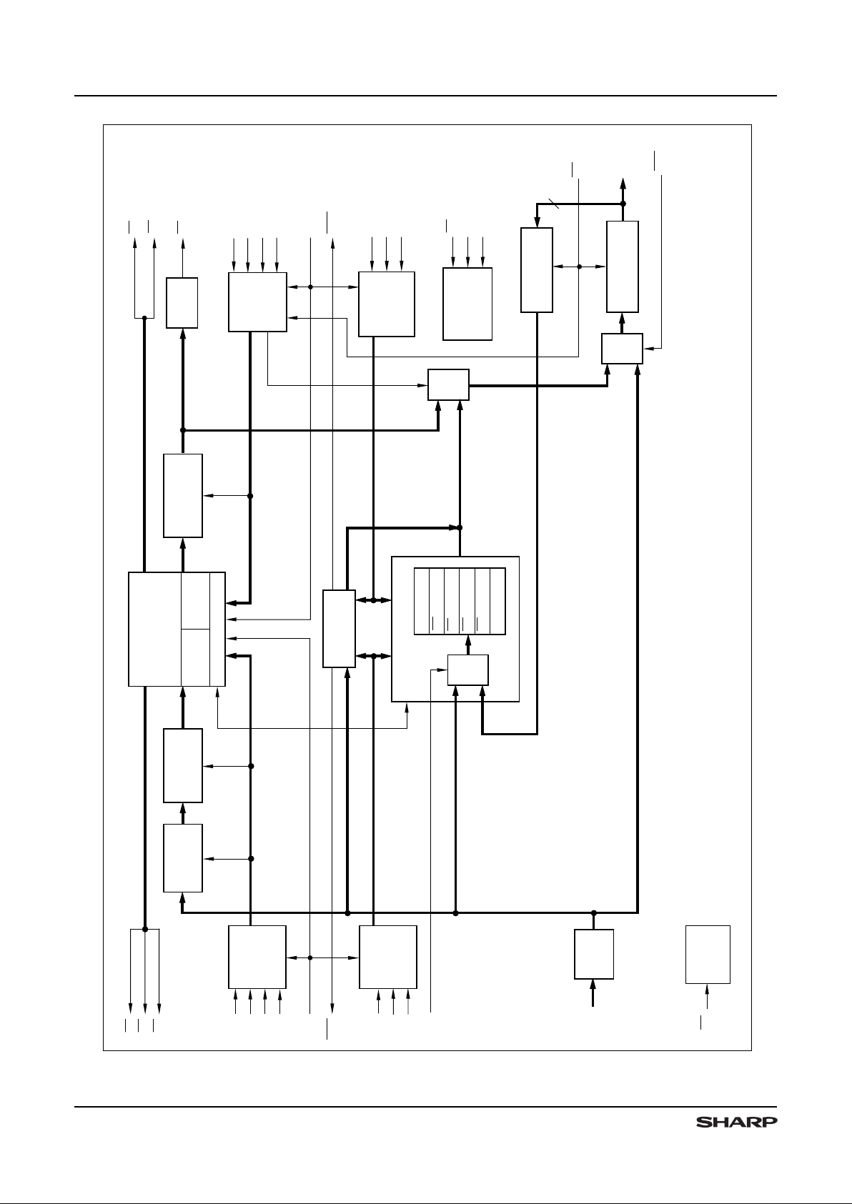
RESET
LOGIC
INPUT
PORT
RS
MAILBOX
OUTPUT
PORT
LOGIC
D[35:0]
ADI
0
ENI
2
ENI
1
CKO
ENO
1
ENO
2
ADO
0
WSO0WSO
1
ADO1ADO
2
WSI
0
FIFO
MEMORY ARRAY
1024 x 36
WRITE
POINTER
READ
POINTER
STATUS FLAGS
CONTROL
AE OFFSET
AF OFFSET
RT OFFSET
RT BASE
PARITY
MUX
RESOURCE REGISTERS
BUS
SWITCHING
(FUNNELING)
PARITY
GENERATOR
BUS
SWITCHING
(DEFUNNELING)
PARITY
CHECK
MUX
OUTPUT PORT
OUTPUT BUFFER
OUTPUT PORT
INPUT BUFFER
OE
Q[35:0]
MEF
PF
INPUT
PORT
LOGIC
ADI1ADI
2
FF
AF
HF
CAPR
BYE
RESOURCE
REGISTER
OUTPUT
LOGIC
MUX
RESOURCE
REGISTER
INPUT
LOGIC
WSI
1
CKI
MFF
EF
AE
RETRANSMIT
LOGIC
RT
RTMD0RTMD
1
543620-6
16 (Q [15:0])
Figure 1. LH543620 Block Diagram
LH543620 1024 × 36 Synchronous FIFO
2
Page 3

PIN DESCRIPTIONS (SUMMARY)
PIN NAME
PIN
TYPE *
DESCRIPTION
DATABUS
D[35:0 ]
I
36-Bit Input-Port Databus
Q[15:0]
I/ O/ Z
Th ree -St ate 36- Bit Outpu tPort Databus
Q[35:16]
O/Z
CLOCKS
CKI
I
Input-Port Clock
CKO
I
Out put-Port C loc k
ASYNCHRONOUS CONTROL
RS
I
Master Reset
OE
I
Output Enable
BYE
I
Data-Bypas s Enable
CAPR
I
Comm and- Addr ess Por t
Refer ence
CONTROL SIGNALS SYNCHRONOUS
TO THE INPUT CLOCK
ENI1,ENI
2
I
Input-Por t Enables
ADI[2:0]
I
Input- Port Address
WSI[1:0]
I
Input-Por t Word-Width
Selection
STATUS FLAGS SYNCHRONOUS
TO THE INPUT CLOCK
FF
O
Full Flag
AF
O
Almost-Full Flag
HF
1
O
Half-Fu ll Flag
MFF
O
Mailbox-Full F lag
PIN NAME
PIN
TYPE *
DESCRIPTION
CONTROL SIGNALS SYNCHRONOUS
TO THE OUTPUT CLOCK
ENO1,ENO
2
I
Output-Port Enables
ADO[2:0 ]
I
Output-Por t Address
WSO[ 1: 0]
I
Out put-Por t W o rd -Width
Se lection
R TMD[1: 0]
I
Retransmit Mode Control
RT
I
Retransmit
STATUS FLAGS SYNCHRONOUS
TO THE OUTPUT CLOCK
AE
O
Almost-Empty Flag
EF
O
Empty Flag
PF
O
Parity-Error Flag
MEF
O
Mailbox-Empt y Flag
VOLTAGES AND GROUNDS
V
CC
V
Positive Power
V
SS
V
Ground
* I = Input, O = Output, V = Voltag e , Z = High-Impedance
1. The half-full flag is user-selectable to be synchronize d to either
CKI or CKO.
1024 × 36 Synchronous FIFO LH543620
3
Page 4
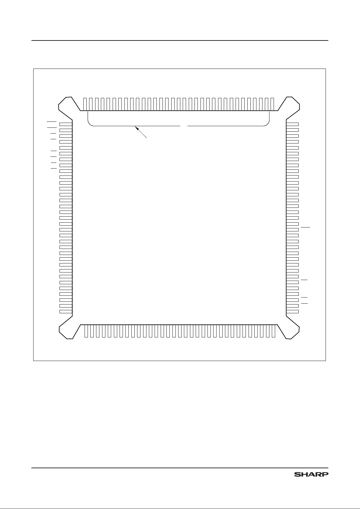
PIN CONNECTIONS
116
115
114
113
112
111
110
109
108
107
106
105
104
103
102
101
100
99
98
97
96
95
94
93
92
91
90
89
88
87
86
85
84
18
19
20
21
22
23
24
25
26
27
28
29
30
31
32
33
34
35
36
37
38
39
40
41
42
43
44
45
46
47
48
MEF
MFF
EF
AE
V
SS
HF
AF
FF
CKO
Q
35
Q
30
Q
28
Q
27
Q
25
Q
24
Q
23
Q
22
PF
V
SS
V
CC
V
SS
49
50
Q
31
515253545556575859606162636465666768697071727374757677787980818283
D
29
D
30
D
31
D
33
D
34
D
35
ENI
1
ENI
2
ADI
0
ADI
2
WSI
0
WSI
1
BYE
ENO
1
ADO
0
ADO
1
ADO
2
WSO
0
WSO
1
RS
RTMD
1
RT
OE
V
CC
ADI
1
CAPR
ENO
2
V
CC
RTMD
0
V
CC
17
16151413121110
9876543
2
Pin 1
Pin 132
131
130
129
128
127
126
125
124
123
122
121
120
119
118
117
D
0D1D2
D
3
D4D5D6D8VSSD9D
11
D
12
D25D
26
D
10
D
27
V
CC
Q
20
Q
19
Q
17
Q5Q
4
Q
2
V
SS
Q
1
Q
0
543620-4
D
7
D13D
14
V
CC
V
CC
Q
34
V
SS
Q
33
Q
32
V
CC
Q
29
V
CC
Q
26
V
SS
V
CC
Q
18
Q
21
Q
16
V
CC
Q15Q14Q13Q
12
Q
11
Q
10
Q9Q
8
Q
7
Q
6
V
SS
V
CC
V
CC
V
CC
Q
3
V
SS
V
SS
D
32
D
28
V
SS
V
CC
D15D16D17CKI
D18D19D20D21D22D23D
24
V
SS
V
SS
V
SS
TOP VIEW
CHAMFERED
EDGE
132-PIN PQFP
Figur e 2. Pin Connections f or 132-Pin PQFP Package
(T op Vi ew )
LH543620 1024 × 36 Synchronous FIFO
4
Page 5

PIN LIST
PIN NAME PIN NO.
D
14
1
D
13
2
D
12
3
D
11
4
D
10
5
D
9
6
D
8
8
D
7
9
D
6
10
D
5
11
D
4
12
D
3
13
D
2
14
D
1
15
D
0
16
MEF 18
MFF
19
EF
20
AE
21
HF
23
AF
24
FF
25
PF
26
CKO
27
Q
35 29
Q
34
30
Q
33
32
Q
32
33
Q
31
35
Q
30
36
Q
29
38
Q
28
39
Q
27 41
Q
26
42
Q
25
44
Q
24
45
Q
23
47
Q
22
48
Q
21
52
Q
20
53
Q
19 55
Q
18
56
Q
17
58
Q
16
59
PIN NAME PIN NO.
Q
15
61
Q
14
62
Q
13
64
Q
12
65
Q
11
67
Q
10
68
Q
9
70
Q
8
71
Q
7
73
Q
6
74
Q
5
76
Q
4
77
Q
3
79
Q
2
80
Q
1
82
Q
0
83
OE
85
RT
86
RTMD
1
87
RTMD
0
88
RS
89
WSO
1
90
WSO
0
91
ADO
2
93
ADO
1 94
ADO
0
95
ENO
2
96
EN0
1
97
BYE
98
CAPR
99
WSI
1
101
WSI
0
102
ADI
2 103
ADI
1
104
ADI
0
105
ENI
2
106
ENI
1
107
D
35
109
D
34
110
D
33
111
D
32 112
D
31
113
D
30
114
D
29
115
PIN NAME PIN NO.
D
28
116
D
27
117
D
26
119
D
25
120
D
24
121
D
23
122
D
22
123
D
21
124
D
20
125
D
19
126
D
18
127
CKI
128
D
17
130
D
16
131
D
15
132
V
SS
7
V
CC
17
V
SS
22
V
CC
28
V
SS
31
V
CC
34
V
SS
37
V
CC
40
V
SS
43
V
CC 46
V
SS
49
V
SS
50
V
CC
51
V
CC
54
V
SS
57
V
CC
60
V
SS
63
V
CC 66
V
SS
69
V
CC
72
V
SS
75
V
CC
78
V
SS
81
V
CC
84
V
CC
92
V
SS 100
V
CC
108
V
SS
118
V
CC
129
1024 × 36 Synchronous FIFO LH543620
5
Page 6

ABSOLUTE MAXIMUM RATINGS
1
PARAMETER RATING
Supply Voltage to VSS Potential –0.5 V to 7 V
Signal Pin Voltage to VSS Potentia l
2
–0.5 V to VCC + 0.5 V
DC O utput Cu rrent
3
± 75 mA
Stor age Temp era tur e Range –65oC to 150oC
Power Dissipat io n (Package Limit ) 2.5 Wat ts (Quad Flat Pack)
NOTES:
1. Stresses greater than those listed under ‘Absolute Maximum Ratings’ may cause permanent damage to the device. This is a stress rating for
transient conditions only. Functional operation of the device at these or any other conditions outside those indicated in the ‘Operating Range’
of this specification is not implied. Exposure to absolute maximum rating conditions for extended periods may affect reliability.
2. Negative undershoot of 1.5 V i n amplitude is permitted for up to 10 ns, once per cy cle.
3. O utp uts should not be shorted f or more than 30 seconds. No more than one output should be shorted at any time.
OPERATING RANGE
SYMBOL PARAMETER MIN MAX UNIT
T
A
T emper ature, Ambient
070
o
C
VCCSupply V olta ge
4.5 5.5 V
V
SS
Supply V olta ge
00V
VILLogic LOW Input V oltag e
1
–0.5 0.8 V
V
IH
Logic HIGH Input Volt age
2.2 Vcc + 0.5 V
NOTE:
1. Negative undershoot of 1.5 V i n amplitude is permitted for up to 10 ns, once per cy cle.
DC ELECTRICAL CHARACTERISTICS (O ver Operating Range)
SYMBOL PARAMETER TEST CONDITIONS MIN TYP MAX UNIT
I
LI
Input Le akage Cur rent VCC = 5.5 V, VIN = 0 V T o V
CC
–10 10
µA
I
LO
I/O Leakage Current
OE ≥ VIH, 0 V ≤ V
OUT
≤ V
CC
–10 10
µA
V
OL
Logic LOW Output Volt age IOL = 16. 0 mA
0.4 V
V
OH
Logic HIGH Outpu t Volt age IOH = –8.0 mA
2.4 V
I
CC
Average Supply Current
1,2
Measur ed at fC = maximum
205 380 mA
I
CC2
Average St andby Supply Current
1,3
All Input s = V
IHMIN
(Clock idle)
40 85 mA
I
CC3
Power-Dow n S upply Current
1
All Input s = VCC,
Out put s – open,
Contro l – deasserted,
Clocks = V
CC
0.01 1.0 mA
NOTE:
1. ICC, I
CC2
, and I
CC3
are dependent upon actual output loading, and ICC is also dependent on cycle times.
Specified values are with outputs open (for ICC: CL = 0 pF); and, for ICC, operating at minimum cycle times.
2. ICC (MAX): Using worst case conditions and data pattern. ICC (TYP): Using VCC = 5 V and average data pattern.
3. I
CC2
(TYP): Using VCC = 5 V and TA = 25°C.
LH543620 1024 × 36 Synchronous FIFO
6
Page 7
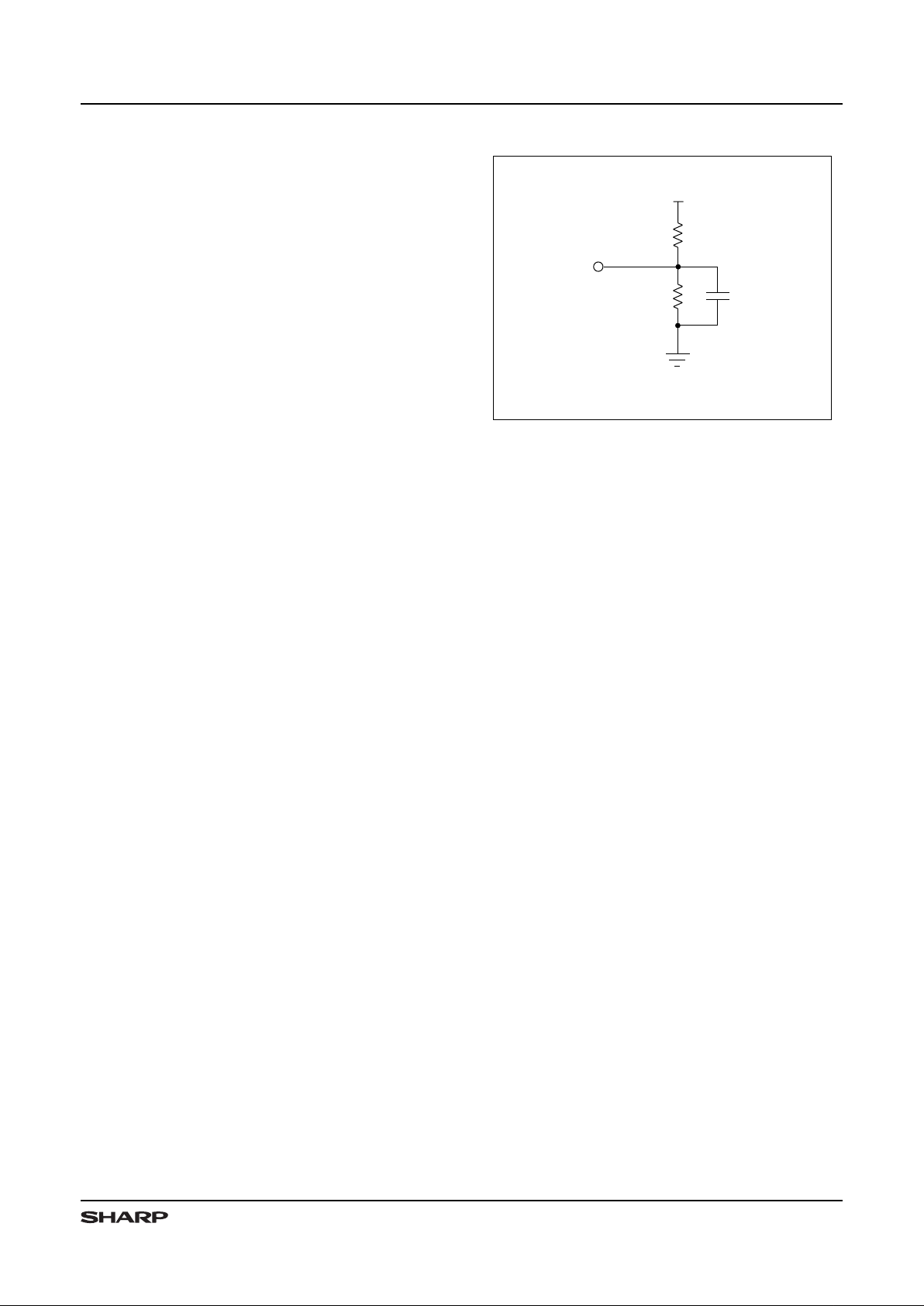
AC TEST CONDITIONS
PARAMETER RATING
Input Pulse Leve ls
VSS to 3 V
Inpu t Rise and Fall Times (10% to 90% )
3 ns
Output Re ference Levels
1.5 V
Input Timing Reference Levels
1.5 V
Output Load , Timin g T es ts
Fig ure 3
CAPACITANCE
1,2
PARAMETER RATING
CIN MAX. (Input Capacitance)
8 pF
C
OUT
MAX. (Output Capacit ance)
10 pF
NOTES :
1. Sample tested only.
2. Capacitances are maximum values at 25oC,
measured at 1.0 MHz, with VIN = 0 V.
543620-27
INCLUDES JIG AND SCOPE CAPACITANCES
*
DEVICE
UNDER
TEST
+5 V
30 pF
1.1 k Ω
680 Ω
*
Figur e 3. Output Load Circui t
1024 × 36 Synchronous FIFO LH543620
7
Page 8

AC ELECTRIC AL CHARACTERIST ICS 1 (See Timing Diagrams Pages 21-35)
SYMBOL DESCRIPTION
–20 –25 –30
UNIT
MIN MAX MIN MAX MIN MAX
f
C
Clock Cycle Frequency 50 40 33 MHz
t
C
Clock Cycle Time 20 25 30 ns
t
CH
Clock HIGH Time 8 10 12 ns
t
CL
Clock LOW Time 9 12 14 ns
t
DS
Data In Setup Time
567ns
t
DSO
Data Setup Time When Writing to Resource
Register From Output Port
10 12 14 ns
t
DH
Data In Hold Time 2 2 2 ns
t
DHO
Data Hold Time When Writing to Resource Register
From Output Port
222ns
t
A
Data Out Acc ess T im e 14 16 18 ns
t
OH
Data Out Hold Time
444ns
t
ES
Enable Setup Time 5 6 7 ns
t
EH
Enable Hold Time 2 2 2 ns
t
OES
Outp ut Enab le Setu p Ti me 6 7 8 ns
t
OEH
Outp ut Enab le Hold Tim e 2 2 2 ns
t
OL
OE to Data Out Low-Z
2
111ns
t
OZ
OE to Data Out High-Z
2
12 15 19 ns
t
OE
OE to Data Valid 10 12 14 ns
t
EF
Empt y Flag Acces s T ime
14 16 18 ns
t
FF
Full Flag Access Time 14 16 18 ns
t
AE
AE Fla g Acces s T ime 14 16 18 ns
t
AF
AF Fla g Acce ss T ime 14 16 18 ns
t
HF
HF Fla g Acce ss T ime 14 16 18 ns
t
PF
Pari ty Fla g Acce ss T im e
14 16 18 ns
t
MFF
Mail box FF Ac cess T ime 14 16 18 ns
t
MEF
Mail box EF Ac cess T ime 14 16 18 ns
t
AS
Addr ess Setu p T ime 10 12 14 ns
t
AH
Addr ess Hold Ti me 2 2 2 ns
t
WSS
WSI and WSO Setup T ime 10 12 14 ns
t
WSH
WSI and WSO Hold Ti me 2 2 2 ns
t
RTMS
Retransmit Mode Setup Time 5 6 7 ns
t
RTMH
Retr ansm it Mod e Hold T ime
222ns
t
RTS
Retr ansm it Setu p T ime 5 6 7 ns
t
RTH
Retr ansm it Hold Ti me 2 2 2 ns
t
RS
Reset Pulse Width 20 25 30 ns
t
RSR
Reset Recovery Time
2
10 12 15 ns
t
RF
Reset LOW to Flag Valid 30 35 40 ns
t
RO
Reset to Data Out LOW 18 20 22 ns
t
BA
Bypass LOW to Data Valid 12 16 18 ns
t
BD
Bypass Propagation Delay
12 16 18 ns
t
SKEW1
Skew Time Between CKO and CKI for FF
3
7911ns
t
SKEW2
Skew Time Between CKI and CKO for EF
4
7911ns
t
SKEWM
Skew Time Between Clock for Mailbox Flags 7 9 11 ns
NOTES:
LH543620 1024 × 36 Synchronous FIFO
8
Page 9
PIN NAME DESCRIPTION
DATABUS
D[35:0]
36-bit Input-Port Databus. The D port is the input port for the FIFO memory array, the resource
registe rs, and the mailbo x, or it may be directly connected to the output port. See F igure 4.
D[35:0] is sync hronous t o the rising edge of CKI.
Q[35:0]
Three-St at e 36-Bit Output -Por t Databus. Th e Q port is the out put port for the FIFO memor y array,
the resourc e reg iste rs, and the ma ilbo x, or it may be directly connect ed to the input port. See Figure
4. Q[35:0] is synchronou s to the risin g edge of CKO. The lower 16 bits of the Q port (Q[15: 0]) may
also be used as the input port for the resourc e register .
CLOCKS
CKI
Input-Port Clock. CKI is a free-running wavef or m controlled by an osc illator . It may be irre gular or
asynchronous i f minimum clock-HIGH times and clock- LOW t imes are met.
CKO
Output-Port Clock. CKO is a fr ee-running wavef orm controlled by an oscillator. It may be irregular
or asynchrono us if minimum clock-HIG H times and cloc k-LOW tim es ar e met.
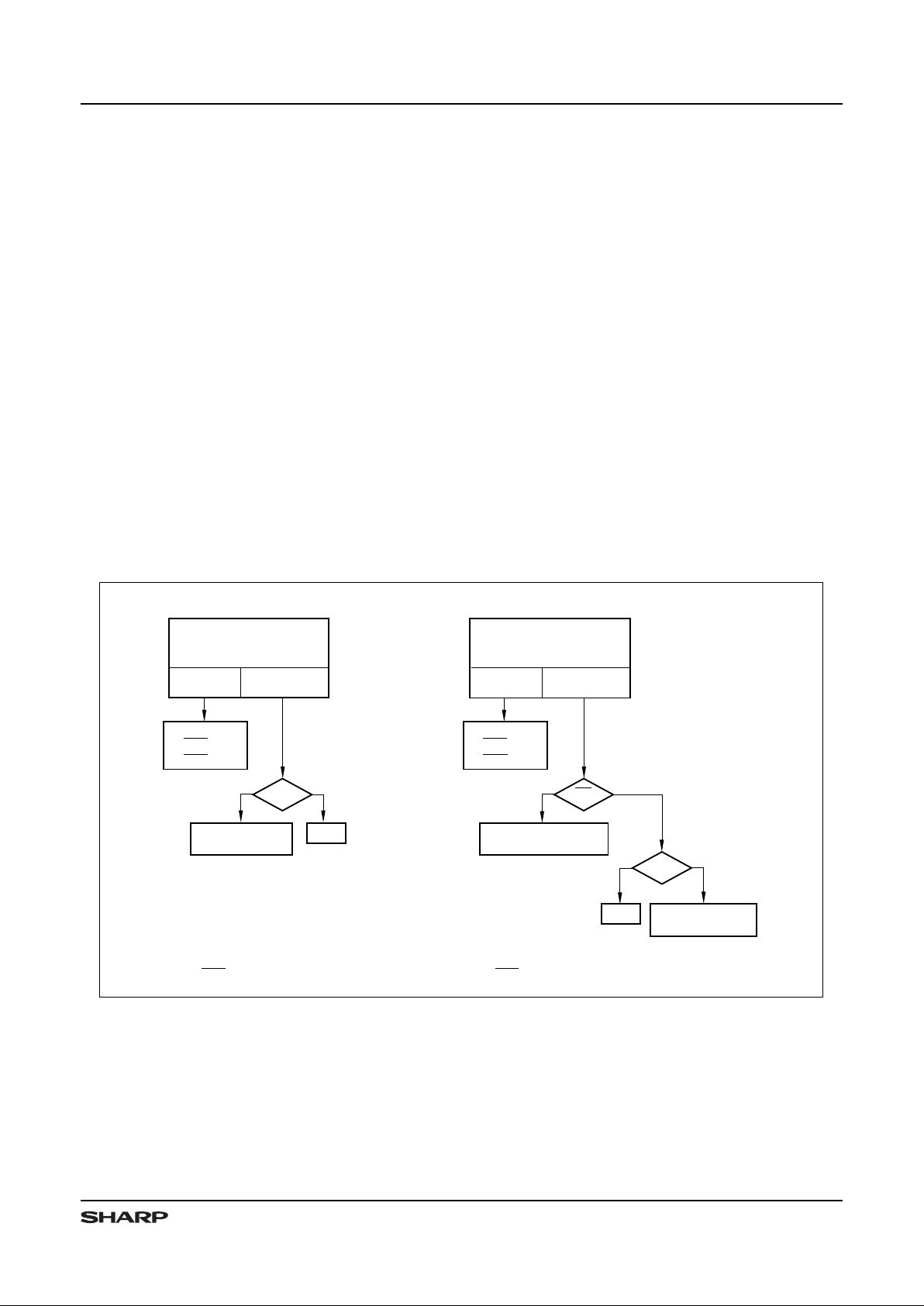
PIN DESCRIPTIONS (FUNCTIONAL)
CAPR
D → MAILBOX
MFF = L
MEF = H
IDLE
*
All the operations are synchronized to CKI,
except MEF is set HIGH on CKO.
*
All the operations are synchronized to CKO,
except MFF is set HIGH on CKI.
543620-5
SELECT INPUT
PORT FUNCTION
ADI [2:0] =
MAILBOX
RESOURCE
REGISTER
OE
MAILBOX → Q
MFF = H
MEF = L
RESOURCE
REGISTER (ADO) → Q
SELECT OUTPUT
PORT FUNCTION
ADO [2:0] =
MAILBOX
CAPR
Q → RESOURCE
REGISTER (ADO)
LH L H
LH
D → RESOURCE
REGISTER (ADI)
RESOURCE
REGISTER
IDLE
INPUT PORT
OUTPUT PORT
Figure 4. Resource Register s, Read and Write
1024 × 36 Synchronous FIFO LH543620
9
Page 10

Table 1. I nput- P ort Address
ADI2ADI1ADI
0
SELECTION
DEFAULT VALU E
(of the selected
REGISTER)
L L L RBASE register
0
LLH
ROFFSET
register
0
LHLA F off set value
8
L H H Parit y register
0
HL LAE offset value
8
HL HControl register 1
H H L Mailbox
0
HHH
Resource
regist ers writ e
disabled
T abl e 2. Input- Por t Word- Wi dt h Selecti on
WSI1WSI
0
FU NCTION
LL
9-B it Data -Path
Width
Input data D[8:0]
LH
18-Bit Dat a-Pat h
Width
Input dat a D[17:0]
HL
Reserved
HH
36-Bit Dat a-Pat h
Width
Input dat a D[35:0]
PIN NAME DESCRIPTION
ASYNCHRONOUS CONTROL
RS
Master Reset. When asser t ed LOW , the LH543620 int ern al reso urce regis ters are set to their
default value. See Table 1. The stat us flags indicate Emp ty FIFO.
OE
Output Enable. Whe n asserted LOW, OE forces Q[35:0] to be active. When deasser ted HIGH, OE
forces Q[35:0] into a Hi-Z state. Bit 6 of the control regis ter gove rns whether OE suppr esses the
advancement of the Read Pointer (RP). In this case, OE must obey setup time and hold time
relative t o CKO.
BYE
Data-Bypass Enable. When asser te d LOW, BYE conn ect s Q[35:0] directly to D[35:0].
CAPR
Command-Address Port Reference. CAPR determ ines the source of the 16-bit word t o be loaded
into the resource regist er. Whenev er CAPR is LOW, the word comes from the Input Port. Whenever
CAPR is HIGH (OE is HIGH), the word comes from the Output Port.
NOTES:
1. The destination of the resour ce reg iste r is always t he Outp ut Port .
2. CAPR is assumed to be a steady signal. It is not allowed to change ‘on- the-fl y’ during operation .
CONTROL SIGNALS SYNCHRONOUS TO THE INPUT CLOCK
ENI1, ENI
2
Input-Port Enables. ENI1 and ENI2 are active HIGH and synch ron ous to the rising edge of C KI.
Data is written into the FIFO memor y array when both ENI1 and ENI2 are asserted HIGH.
NOTE: ENI1, ENI2 DO NOT ENABLE writing data into the Resour ce Registers or the Mailbox.
ADI[2:0]
Input- Port Ad dress. ADI [2 :0] sp ecifies the In put-Port destination. Se e Table 1. ADI [ 2:0 ] is
synchro nized to the rising edge of CKI.
WSI[1:0]
Input- Port Word-Widt h Se lection. WSI[1:0] selects the Inp ut-Por t Wor d-Widt h. See Table 2.
WSI[1:0] is synchron ous t o the rising edge of CKI.
LH543620 1024 × 36 Synchronous FIFO
10
Page 11

T able 3. HF Synchronization Modes
CONTROL
REGISTER
FUNCTION
BIT 4 BIT 3
L * L * Asynchr onous Mode: HF
LH
Synchronous Mode I: HF is
synchr onou s to the risin g edge of CKO
HL
Synchronous Mode II: HF is
synchr onou s to the risin g edge of CKI
HH
* Default Mode
T abl e 4. Out put -Por t Address
ADO2ADO1ADO
0
SEL ECTION
DEFAULT VAL UE
(of the selected
REGISTER)
LLL
RBASE
register
0
LLH
ROFFSET
register
0
LHL
AF offset value
8
L H H Parity re giste r 0
HLL
AE offset value
8
HLH
Control
regis ter
1
HHL
Mailbox
0
HHH
Resour c e
regis ters r ead
disabled
Not applicable
PIN NAME DESCRIPTION
STATUS FLAGS SYNCHRONOUS TO THE INPUT CLOCK
FF
Full Flag. FF is synchronous to the rising edge of CKI. When asserted LOW , 1024 36-bit words of
the FIFO memo ry arr ay contain m eaningf ul dat a. When FF is asser t ed, writing da ta to the FIFO is
disabled.
AF
Almost-Full Flag. When asserted LOW , AF indica tes that t her e are at mo st ‘p’ vacant 36-bit
words remaining in the FIFO memory array, where ‘p’ is the value of the Alm ost-Fu ll-Of fset-Value.
AF has t wo synchronization modes depending on Bit 5 of the contro l register.
Bit 5 = 0
(Default ) Asynchr onou s Mode
Bit 5 = 1
: AF is synchr onou s to the rising edge of CKI.
HF
Half-Ful l Flag. When asserted LO W , ther e are at least 513 36-bit words in the FIFO memor y
array. HF has three synchroniza tion modes depending on Bits 3 and 4 of the control register. See
Table 3.
MFF
Mailbox-Full Fla g. MFF is synchronized to th e rising edge of CKI. When assert ed LOW, it
indicates that a new mail word has been placed in the mailbox.
CONTROL SIGNALS SYNCHRONOUS TO THE OUTPUT CLOCK
ENO1, ENO
2
Output - Port Enables. ENO1 and ENO2 are active HIGH, sync hr onous to the rising edg e of CKO.
Data is read fro m the FIFO memo ry array when bot h ENO1, ENO2 are a sserted.
NOTE: ENO1, ENO2 DO NOT ENABLE reading data from the Resource Registe r or the Mailbox.
ADO[2:0]
Output -Port Address. ADO[ 2: 0] specifies the Output-Port source/destination. See Table 4.
ADO[2: 0] is synchr onou s to the risin g edge of CKO.
NOTE: In order to read the resour ce regist er at the out put bus, BYE sho uld be deasserted and the
FIFO memory array sho uld be disabled.
1024 × 36 Synchronous FIFO LH543620
11
Page 12

Table 5. Output -Port Word-Width Selection
WSO1WSO
0
FUNCTION
LL
9-B it Data-Path
Width
Out p ut d a ta Q [ 8:0]
LH
18-Bit Dat a- Path
Width
Out p ut d a ta Q [ 17:0]
HL
36-Bit Dat a- Path
Width Wit h Byt eOrder-Rever sa l
Out p ut d a ta Q [ 35:0]
HH
36-Bit Dat a- Path
Width
Out p ut d a ta Q [ 35:0]
T able 6. Retra nsmi t Oper atio n Modes
RTMD1RTMD0OPERATION ACTION TAKEN
LL
Depth
Cascade
Mode
The Alm ost-Empt y
Flag is a handsh ake
signal for cascading
LH
Retransmit
(RBASE) +
(ROFFSET) → RP
HL
Retransmit
and Mark
(RBASE) +
(ROFFSET) → RP
and
(RBASE) +
(ROFFSET) →
RBASE
HH
Mark (RP) → RBASE
PIN NAME DESCRIPTION
CONTROL SIGNALS SYNCHRONOUS TO THE OUTPUT CLOCK (cont’d)
WSO[1:0]
Output-Port Word-Width Selection. WSO[ 1:0] is synchr onous to the rising edge of CKO.
WSO[1:0] selects the O utput -Por t Wor d-Widt h and cont r ols byte- ord er-r ever sal acco rding to
Tab le 5.
RTMD[1:0]
Retransm it Mode Contr ol. RTMD[1:0] is synchr onized to the rising edge of CKO. RTMD[1:0 ]
contr ols the plac ement of new contents int o the Read Pointer (RP) and/or the Ret rans mit Base
(RBASE) regist ers. Wheneve r Retransm it (RT) is assert ed, one of three operat ions is performed
according t o the setting of RTMD[1: 0] . See Table 6.
NOTES:
1. When RTM D[1: 0] is set to 0, the FIFO is in depth cascade mode, and the Ret ran smit
mechanism can not be used. In cascade m ode, the Almost -Empt y Flag is a han dshake signal f or
cascading. The Almost-Empt y Flag is used as an input to the ENI of the next FIFO in the chain.
2. In standard FIFO operation RTMD[ 1:0] must not be set to 0 and the Retransmit signal mus t be
HIGH.
RT
Retransm it. RT is synchronized t o the rising edge of CKO. When asser t ed LOW , RT causes one
of the Retransm it Mode operat ions to be perfor med, according to the encoding of RTMD[1: 0] . See
Tab le 6.
NOTE : When RTM D[ 1:0 ] = 0 (FIFO is in cascade mo de) RT is ignored.
LH543620 1024 × 36 Synchronous FIFO
12
Page 13

OPERATIONAL DESCRI PT ION
The LH543620 has four operating modes: Normal
Mode, Pro grammable Res our ce Reg isters, Mailbox, and
Data Bypass.
NORM AL MO DE
Normal FIFO operation refe rs to Read and Write operati ons to t he FIFO memor y array . Data W rite oper atio ns
into the FIFO memory array occur at the rising edge of
CKI. The oper ation is enabled if both ENI1 and ENI2 are
asserted HIGH. Data Read operations from the FIFO
memo ry occur at the rising edge of CKO. The operation
is enabled if both ENO1 and ENO2 are asserte d HI GH.
The FIFO write and r ead ope rations a re suppor t ed by
the following mechanisms: Byte- Order-Rever sal and Bus
Funneling/Defunn eling Functions, Status Flags, Retransmit Mechanism, Par ity Ch ecking, and Parity Gener ation.
PIN NAME DESCRIPTION
STATU S FLAGS SYNCHRONOUS TO THE OUTPUT CLOCK
AE
Almost-Empty Flag. The AE flag has two modes of oper ation depending on the RTMD[1:0]
sett in g.
1. RTMD[1:0] ≠ 0: AE is a stand ard Al m ost -Em pt y Flag. When asser ted LOW , AE implies that
ther e are at mo st ‘q ’ 36-b it wor ds in the FIFO memory ar r ay, where ‘q ’ is Alm ost - Empt y- Of fs etValue regist er value. In this mode A E has two synchr onizat ion opt ions dep ending on t he sett in g of
Bit 2 of the c o ntrol re gist er.
Bit 2 = 0
(Default ) Asynchr onou s Mode
Bit 2 = 1
Synchro nous M ode: AE is synchronous to the rising edge of CKO.
2. RTMD[1:0] = 0: AE is a handshake signal for cascad ing.
EF
Empty Fl ag. EF is synch ron ous to the rising edge of CKO. When asserted LO W, all 1024
36-bit words ar e vacant. When asser t ed, EF disables the FIFO Re ad oper at io n.
PF
Parit y- Err or Flag. P F is synchron ized to the r ising edge of CKO. When asser ted LOW , PF
implies that a par ity error has occurr ed in at least one 9-bit byte within a 36- bit w or d read from th e
FIFO memory array. If the re are no errors, it is deasserted HIGH. When an error is detected, the
parity check r esult of each 9-b it byte of the 36 -bit out put word is writ ten to t he par ity register. The
content of the parity re gis ter is froze n unt il read. The PF sig nal is delayed by one CKO cycle
compared to the output data (i.e., if the PF is asserted, ther e was an error in the previous word) .
MEF
Mailbox- Empt y Flag. MEF is synchr ono us to the r is ing edge of CKO. When ass erted LOW , MEF
indicates that the re is no new mail word in the mailbox.
VOLTAGES AND GROUNDS
V
CC
Positive Pow er .
V
SS
Ground.
1024 × 36 Synchronous FIFO LH543620
13
Page 14

Byte-Order-Reversal and Bus Funneling/
Defunneling Functions
Word width can be selected at the Input Port and/or
the Output Port to be 36, 18 or 9 bits wide. When the
Output Port width is selected to be 36 bits, it is possible
to select Byte-Order-Reversal.
The funneling mechanism is controlled by the inputs
WSI[1:0] and WSO[1:0] according to Tables 2 and 5. Data
is packed and unpacked from a 36-bit word memory array.
T able 7 describes all combi nations of funneling /defunnelin g.
Changes to the funneling/defunneling settings during
system opera tion should be made one clock before a
word boundar y, as shown in Example 3.
Example 1: 36-to-9 Funneling
CONDITIONS
RESULTS
WSI[1:0] WSO[1:0]
3–
Input 36 bits wide.
–0
Output 9 bits wide.
Pins used are Q[8:0] .
The dataflow struct ure is illustr ated by Figure 5.
Examp le 2: 18-to-36 Defunneling W ith Byte Reversal
Th is exam ple per form s two funct ions:
1. Bus width change
2. Big Endian to Little Endian conv ersio n
Th is configur ation can be used for connect ing the Intel
80286 t o the Motorola 68040.
CONDIT IONS
RES U L TS
WSI[1:0] WSO[1:0]
1–
Input 18 bits wide.
Pins used ar e D[17: 0] .
–2
Output 36 bits wide with byte
order rever sal.
The dataflow struct ure is illustrated by Figure 6.
Example 3: Changing Input Bus Width From 9 to 36
During O perat ion
CKI WSI ACTION
00
Write 1st 9-bit byte
10
Write 2nd 9-bit byte
20
Write 3rd 9- bit by te
33
Write 4th 9-bit byte
43
Write 1st 36-bit word
T abl e 7. Bus Funneling/Defunnel i ng *
INPUT OUTPUT
CKI WSI = 0 CKO WSO = 3 WSO = 2 WSO = 1 WSO = 0
cycles D[35:9] D[8:0] cycles Q[35:0] Q[35:0] Q[35:18] Q[17:0] Q[35:9] Q[8:0]
0 xxx B0 0 B3 B2 B1 B0 B0 B1 B2 B3 B3 B2 B1 B0 B3 B2 B1 B0
1 xxx B1 1 B7 B6 B5 B4 B4 B5 B6 B7 B1 B0 B3 B2 B0 B3 B2 B1
2 xxx B2 2B7B6B5 B4 B1 B0 B3 B2
3 xxx B3 3B5B4B7 B6 B2 B1 B0 B3
4 xxx B4 4 B7B6B5 B4
5 xxx B5 5
6 xxx B6 6
7 xxx B7 7
8 xxx B8 8
WSI = 1 WSO = 3 WSO = 2 WSO = 1 WSO = 0
D[35:18] D[17:0] Q[35:0] Q[35:0] Q[35:18] Q[17:0] Q[35:9] Q[8:0]
0xxB1 B0 0 B3 B2 B1 B0 B0 B1 B2 B3 B3 B2 B1 B0 B3 B2 B1 B0
1xxB3 B2 1 B7 B6 B5 B4 B4 B5 B6 B7 B1 B0 B3 B2 B0 B3 B2 B1
2xxB5 B4 2B7B6B5 B4 B1 B0 B3 B2
3xxB7 B6 3B5B4B7 B6 B2 B1 B0 B3
4xxB9 B8 4 B7B6B5 B4
WSI = 3 WSO = 3 WSO = 2 WSO = 1 WSO = 0
D[35:0] Q[35:0] Q[35:0] Q[35:18] Q[17:0] Q[35:9] Q[8:0]
0 B3 B2 B1 B0 0 B3 B2 B1 B0 B0 B1 B2 B3 B3 B2 B1 B0 B3 B2 B1 B0
1 B7 B6 B5 B4 1 B7 B6 B5 B4 B4 B5 B6 B7 B1 B0 B3 B2 B0 B3 B2 B1
B7 B6 B5 B4 B1 B0 B3 B2
B5 B4 B7 B6 B2 B1 B0 B3
B7 B6 B5 B4
* NOTE: B0, B1, . . ., represent data bytes.
LH543620 1024 × 36 Synchronous FIFO
14
Page 15

543620-30
B3
BYTE #4
B7
BYTE #8
B2
BYTE #3
B6
BYTE #7
B1
BYTE #2
B5
BYTE #6
B0
BYTE #1
B4
BYTE #5
D35
D27
D26
D18
D17
D9
D8
D0
Q35
Q27
Q26
Q18
Q17
Q9
Q8
Q0
LH543620
B3
BYTE #4B0BYTE #1B1BYTE #2B2BYTE #3
BYTE #8
B2
BYTE #3B3BYTE #4B0BYTE #1B1BYTE #2
B1
BYTE #2B2BYTE #3B3BYTE #4B0BYTE #1
B0
BYTE #1B1BYTE #2B2BYTE #3B3BYTE #4
BYTE #7
BYTE #6
BYTE #5
012 01234
INPUT: WSI[1:0]=3 OUTPUT: WSO[1:0]=0
CKI CKO
. . . . . .. . .
. . .
. . . . . .. . .
. . .
NOTES:
HEAVY SOLID LINES = Main data path.
SHADED LINES = Not used for this application.
Figure 5. Exampl e of 36-to- 9 Bu s Fu nneling
543620-31
NOT USED
B5
BYTE #6B7BYTE #8
B4
BYTE #5B6BYTE #7
D35
D27
D26
D18
D17
D9
D8
D0
Q35
Q27
Q26
Q18
Q17
Q9
Q8
Q0
LH543620
B0
BYTE #1B4BYTE #5
B1
BYTE #2B5BYTE #6
B2
BYTE #3B6BYTE #7
B3
BYTE #4B7BYTE #8
012 012
INPUT: WSI[1:0]= 1 OUTPUT: WSO[1:0]= 2
CKI CKO
. . . . . .. . .
. . .
. . . . . .. . .
NOT USED
34
B1
BYTE #2B3BYTE #4
B0
BYTE #1B2BYTE #3
3
. . .
NOTES:
HEAVY SOLID LINES = Main data path.
SHADED LINES = Not used for this application.
Motorola 68040
Intel 80286
Figur e 6. Example of 18-to- 36 Bus Defunnel ing
With Byte Order Reversal
1024 × 36 Synchronous FIFO LH543620
15
Page 16

Status Flags
There are five status fla gs:
FF Full Flag
AF Almost-Full Flag
HF Half-Full Flag
AE Almost-Empty Flag
EF Empty Flag
The function ality and the synchronizat ion of the status
flags are detailed in the
Pins Descriptions (Functional)
section. All status flags are generated for 36-bit word
widths, not according to selected input or output port
widths.
Retransmit Mechanism
With standard FIFO operations, every data word can
be read out of the FIFO once. The Retransmit mechanism
allows reading the data more than once by providing
flexible control o f the Read Pointer.
Associated with the Retransmit mechan ism are three
control lines: RTMD[1:0], RT, and two Resource registers: RBASE and ROFFSET .
RTMD[1: 0] set s th e mode of operat ion. See Table 6.
RT enables the operation synchronous to CKO.
Retra nsmit allows three modes of operat ion :
Mark: RTMD[1:0] = 3 a nd RT is asserted. The value of
the Read Pointer is saved into the RBASE register.
Retransmit: RTMD[1:0] = 1 and RT is asserted. The
Read Pointer is loaded by the value of RBASE plus the
value of ROFFSET .
R etra nsmi t and Mark : RTMD [1:0 ] = 2 and RT is asserted: The Read Pointer is loaded by the value of RBASE
plus the value of ROFFSET. Then the value of the Read
Pointer is saved into the RBASE regist er .
The t iming of the r etransmit is illustrated in Figures 26
and 27.
When RT is asserted and RTMD[1:0] is set to 1 or 2,
the flags change their value to indicate a ‘Retransmit
state’, i.e., EF, AE, FF deasserted; AF, HF asserted.
Three enable-read cycles are requi red to read the new
data word. The flags r eflect the new status. The retransmit
is acknowledged even when the output is disabled
(ENO = LOW), but enable-read cycles are needed to fill
the pipeline with new infor mation before reading the n ew
data.
NOTES
1. The Retransmit mechanism can be used independent ly and pa ralle l to the write operat ion.
2. RTMD[1:0] must be selected two cycles prior to RT
bein g asser ted and r em ain sta ble during RT low.
3. At least two words need to be in the FIFO memory
arr ay prior t o perfo rm ing a retransm it.
4. When using norm al read and write opera tions, the FF
inhibits writing when the FIFO is full and the EF
inh ibits reading when the FIFO is empt y . This behavior provides a pr otect ion fro m wrapar ound sit uat ions
(i.e., the Read point er is ahead of the Write Pointer).
Th is protectio n is NOT provide d when using r etra nsmit . Th e user should be careful not to write more t han
1024 word s from the m arked point .
5. When the re transmit mechanism is not used, the
reco mmende d connection is:
RTMD[1:0] = 3
RT = HIGH
The Retransmit mechanism can be useful in many
applications. For examp le :
1. Comput er- commun ication s applications.
When t he rec eiver reads a block of data and finds no
errors in the data block, it can mark the beginning of
the new m essage by sett ing the FIFO in MARK mode
R TMD[1: 0] = 3 and asser t the RT signal for one clock
cycle.
If the receiver finds an error in the data block, it can
read the last message again by setting the FIFO in
Retransmit mode RTMD[1:0] = 1 and asserting the
RT signal for one cycle.
2. Overlap add ressing fo r DSP applications.
A typical DSP consists of A/D-FIFO-DSP. In many
applications, the DSP needs to read a block of data
where each block overlaps the previous block (like
the overlap-and-save me thod for filtering.) The overlap addressing can be implemented by using the
LH5 43620 with no additional hardwar e as fol lows:
The FIFO is set to retransmit and mark mode:
R TMD[1:0] = 2, the AF offset register is progr amm ed
to N = Block Size, and the ROFFSET register is
prog ramm ed to (N – Overlap). The d ata is loa ded into
the FIFO each time CK in is triggered.
The DSP can sense the AF flag of the FIFO. Whenever this flag is being asserted, a new block of data
is available in the FIFO. The DSP then read s a block
of da ta, and the n asserts the FI FO’s RT sign al, which
causes the RP and RBASE register to be set at the
beginning of the new block.
LH543620 1024 × 36 Synchronous FIFO
16
Page 17

Parity Checki ng
The Parity chec king mec hanism is always ac tive . Parity checking is done separately fo r each of the 9-bit bytes
of the 36-bit word read from the memory array. Toggling
Bit 0 of the control register selects odd or even parity.
When a parity e rr or is det ect ed in one or m ore bytes, t h e
signal P F is a sser ted and the result of th e individual p arity
checks are wr itt en to the p arit y r egister. See Example 3.
T o avoid a possible in valid PF signal, ENO1 and ENO
2
should not be dea sser ted dur in g the CLKO low time.
The parit y r egist er is frozen until read. W hen read, t he
parity register is released and ready to store the next
parity er r or dat a.
Parit y Gen erat i on
After Reset, parity generation is not active. Parity
generat ion is a ctive only when Bit 1 of the control reg ister
is HIGH. The parity mechanism, when enabled, creates
a parity bit for each of the bytes of the input word. The
parity bit for each byte is created based on its 8 least
significant bits of each 9-bit byt e of the input-data word
and on Bi t 0 of the control r egister (it specif ies odd or even
parity) . The result of the parity generat io n is writt en ba ck
to the MSB of the dat a byt e. See Example 4.
PROGRAMMA BLE RESOURCE REGISTERS
The LH543620 has six progr am m able resou rce registers. The resource registe rs may be loaded from either
the In put Port or the Ou tput Por t. The y can be r ead fr om
the Output Port. The selection and loading or reading of
the resource registers is controlled by ADI, ADO and
CAPR . See Tab les 1 and 4 and Figure 4.
The resour ce register s are:
Contro l (Default = 1).
AE Off set – Off set value of the AE flag (Default = 8) .
AF Offset – Offset value of the AF flag (De fa ult = 8).
RT Offs et – Off set value of the Retr ansmit mechan ism
(De fault = 0) .
RT Ba se – Base regist er of the Retrans mit mechan ism
(De fault = 0) .
Parity
PARI TY CHECK
Q35
Q0
Output word: 100111100 000111100 100111000 000111000
Odd parity: Parity Register = 01 10; PF-Asserted Low
Even parity: Parity Register = 1001; PF-Asserted Low
PARITY GENERATION
D35 D0
Input word: 100111100 000111100 100111000 000111000
Outpu t, odd parity: 100111100 100111100 000111000 00011100 0
Outpu t, even parity: 000111100 00011 1100 100111000 10011100 0
EXAMPLE 3
EXAMPLE 4
1024 × 36 Synchronous FIFO LH543620
17
Page 18

Control Register (See Figur e 7)
After reset, the control register’s value is 1. This sets
the following conditions:
Odd parity
Disabling parity generation (par ity check is act ive) .
AF, HF, AE fla gs are asynch ronous.
OE signal does not control the Read point er.
Read/Write Resource Register Mode
It is possible to write to the resource registers from
either the Inpu t Port or the Out put Port. Reading from the
resource register is possible only from the Output Port.
The source port for the write operation is determined by
the cont ro l signal CAPR.
Input Port:
Data from the Input Port is written to a resource regist er
when:
the value of the input-addre ss field, ADI, select s the
registe r (see Table 1)
CAPR is LOW
The operation is enabled by ADI[2:0] and synchronized
to CKI.
Out put Port:
Data from the Output Port is written to a resource
regis ter when:
the value of the ou tpu t-addr ess field, ADO , selects the
register (see Table 4)
CAPR is HIGH
OE is HIGH
NOTE:
ADI[2:0] should remain stable whenev er data is
com in g in from the out put port.
Data is read from a r esource regist er to the Output Port
when:
the value of the ou tpu t-addr ess field, ADO , selects the
register (see Table 4)
OE is LOW
Both operations are enabled by ADO[2:0] and are
synch ron ous t o CKO.
MAILBOX
The mailbox mechanism includes:
One 36-bit data register.
Two status flags:
– MFF Mailbox Full Flag
– MEF Mailbox Empty Flag
543620-29
6543210
0 EVEN PARITY
1 ODD PARITY
0 PARITY GENERATION IS DISABLED
1 PARITY GENERATION IS ENABLED
0 AE ASYNCHRONOUS
1 AE SYNCHRONOUS TO CKO
0 HF ASYNCHRONOUS
1 HF SYNCHRONOUS TO CKO
2 OR 3 HF SYNCHRONOUS TO CKI
0 AF ASYNCHRONOUS
1 AF SYNCHRONOUS TO CKI
0 OE DOES NOT CONTROL THE READ POINTER
1 OE CONTROLS THE READ POINTER
Figure 7. LH543620 Control Register
LH543620 1024 × 36 Synchronous FIFO
18
Page 19

Writing to the Mailbox is enabled from the Input Port
when the Input Port addr ess field ADI[ 2: 0] = 6. The write
operat ion is synchr ono us to the rising edge of CKI.
When writing to the Mailbox, the status flags are
changed as fo llows:
MEF is deasserted HIGH on the risin g edge of CKO.
MFF is asserted LOW on the risin g edge of CKI.
A Mailbox read is enabled from the Output Port, when
the Output Port address field ADO[2:0] = 6. The Read
operat ion is synchr onized to CKO.
When reading the Mailbox, the status flags are
changed as fo llows:
MEF is asserted LOW on the rising edge of CKO.
MFF is deasserted HIGH on the rising edge of CKI.
After reset the Mailbox is em pty (i.e., MFF = HIGH,
MEF = LOW).
When using Mailbo x, the transmitt er side ca n trans fer
a message to the receiver side without interrupting the
data in the FIFO memory array.
DATA BYPASS MODE
Data Bypass mode is selected when BY E = L OW. In
this mode, data may be transfe rred asynchronously from
the Input Port to the Output Port. The device may be
placed in Data Bypass mode without voiding the cont ents
of the FIFO memory array, the Mailbox Registe r, or the
Resource Register. However, if the input is enabled
(ENI
1,2
= HIGH) then the input data D is also written to
the FIFO memory array on the rising edge of CKI. If the
Output is enabled, (ENO
1,2
= HIGH) then the input data
D is transf erred to the out put bu ffer , and the Read Pointer
is increm ented by CKO . The con trol signal O E is fun ction ing when BYE is assert ed.
The recom mended co ntr ol sett ing for bypass is:
ENI = LOW, ENO = LOW, ADI[2:0] = 7,
ADO[2: 0] = 7, OE = LOW, BYE = LO W
OPERATIONAL MODES AND CONFI GURATIONS
Interlocked Width Expansion (Figure 8A)
Two LH543620s may be configured to expand the
width to 72 bits. This is accomplished by:
Cross-conne ctin g the FF out put of each FI FO to ENI
1
(or ENI2) input of the other FIFO.
Cross-conne cting the EF out put of e ach F IFO t o ENO
1
(or ENO2) input of the other FIFO.
The compo site status flags are the OR fun ction of the
individual flags.
Pipeline Cascading Mode and ‘Two-Dimension’
Pipeline Cascadin g Mode (Figure 8B and 8C)
Depth casc ading is accom plished by:
Setting the upper FIFO into cascade m ode:
RTMD[1:0] = 0
Connecting the same free- running clock t o CKO of the
upper FIFO and to CKI input of the lower FIF O.
Connecting the AE output of t he upper FIFO to ENI
1
input (or ENI2) of the lower FIFO.
Connecting the FF output of the lower FIFO to ENO
1
input (or ENO2) of the upper FIFO.
NOTE:
R TMD[ 1: 0] should remain stab le during cascade
mode oper ation (i. e., rem ain low).
1024 × 36 Synchronous FIFO LH543620
19
Page 20

ENI
1
ENI
2
FF
D[35:0]
CKO
ENO
1
EF
ENO
2
Q[35:0]
CKI
ENI
1
ENI
2
FF
CKO
ENO
1
EF
ENO
2
CKI
ENI
1
ENI
2
FF
CKO
ENO
1
AE
ENO
2
CKI
ENI
1
ENI
2
FF
CKO
ENO
1
EF
ENO
2
CKI
ENI
1
ENI
2
FF
CKO
ENO
1
AE
ENO
2
CKI
ENI
1
ENI
2
FF
CKO
ENO
1
EF
ENO
2
CKI
ENI
1
ENI
2
FF
CKO
ENO
1
AE
ENO
2
CKI
ENI
1
ENI
2
FF
CKO
ENO
1
EF
ENO
2
CKI
A. INTERLOCKED WIDTH EXPANSION
DI[35:0] DO[35:0]
B. PIPELINED CASCADING MODE
V
CC
COMMON
CLOCK
V
CC
COMMON
CLOCK
DI[71:36]
FF
DI[35:0]
DO[71:36]
DO[35:0]
DO[71:36]
DO[35:0]
CKI
ENI
DI[71:36]
DI[35:0]
C. 'TWO-DIMENSION' PIPELINED CASCADING MODE
543620-7
V
CC
CKI
ENI
2
FF
ENI
1
CKI
ENI
EF
CKO
ENO
CKO
ENO
1
EF
ENO
2
FF
EF
CKO
ENO
RTMD[1:0]
L L
RTMD[1:0]
RTMD[1:0]
RTMD[1:0]
H H
RTMD[1:0]
RTMD[1:0]
L L
H H
L L
H H
D[35:0] Q[35:0]
D[35:0] Q[35:0] D[35:0]
Q[35:0]
D[35:0]
Q[35:0]
D[35:0]
Q[35:0]
D[35:0]
Q[35:0]
D[35:0]
Q[35:0]
NOTES:
DI = System data input width.
DO = System data output width.
Figure 8. LH543620 Width and Depth Expansion Schem e
LH543620 1024 × 36 Synchronous FIFO
20
Page 21

t
RF
543620-15
t
RO
t
RF
t
RS
t
RSR
RS
Q[35:0]
ENI
1
, ENI2,
ENO
1
, ENO
2
EF, AE
FF, HF,
AF, PF
1. After reset, the outputs will be LOW if OE = LOW, and in a high-impedance
state if OE = HIGH.
2. The clocks (CKI, CKO) may be free-running during a reset operation.
3. If CAPR = L, then ADO = XXX and ADI must be = H,H,H for proper reset.
If CAPR = H, then ADI = XXX and ADO must be = H,H,H for proper reset.
NOTES:
ADI[2:0]
3
ADO[2:0]
OE = HIGH
1
OE = LOW
Figur e 9. Reset Timin g
TIMING DIAGRAMS
1024 × 36 Synchronous FIFO LH543620
21
Page 22

CKI
CKO
D[35:0]
t
C
CL
t
CH
t
EH
t
t
ES EH
t
t
ES
DH
t
Q[35:0]
DS
t
DH
t
t
C
t
EH
t
EH
t
ES
t
ES
t
OE
t
OL
t
A
PREVIOUS DATA
t
A
t
OH
t
OH
t
OZ
t
OH
ENI1, ENI
2
ENO1, ENO
2
OE
543620-8
t
CH
t
CL
NOTES:
1. Both ENI
1
and ENI2 must be asserted (HIGH) to enable write operations.
2. Both ENO
1
and ENO2 must be asserted (HIGH) to enable read operations.
DS
t
Figu r e 10. Writ e and Re ad Oper at i on
LH543620 1024 × 36 Synchronous FIFO
22
Page 23

CKI
CKO
D[35:0]
EF
543620-9
NOTE: If t
SKEW2
< (minimum specification) then EF may change one CKO cycle later.
t
DS
t
EH
DATA VALID
t
ES
t
DH
t
SKEW2
t
EF
t
EF
t
A
t
OH
DATA-OUT VALID
OE
Q[35:0]
(NOTE)
ENI1, ENI
2
ENO1, ENO
2
Figure 11. Empty Flag Timing
1024 × 36 Synchronous FIFO LH543620
23
Page 24

CKI
CKO
D[35:0]
FF
543620-10
DATA WRITE
t
A
t
OH
DATA READ
Q[35:0]
t
DS
t
DH
t
FF
t
FF
t
ES
t
SKEW1
t
ES
t
EH
NO WRITE
WRITE
(NOTE)
ENI
1
, ENI
2
ENO1, ENO
2
NOTE: If t
SKEW1
< (minimum specification) then FF may change one CKI cycle later.
Figure 12. Full Flag Timing
LH543620 1024 × 36 Synchronous FIFO
24
Page 25

CKO
AF
543620-11
NOTES:
1. The synchronization mode of AF is set by programming bit 5 of control register.
2. When in synchronization mode and t
SKEW1
< (min specification) then AF may change one CKI later.
CKI
AF
t
AF
t
AF
t
AF
t
AF
SYNCHRONOUS MODE
ASYNCHRONOUS MODE
t
SKEW1
WORD (1024 - p-1) WRITE OCCURS WORD (1024 - p-1) READ OCCURS
ENI1, ENI
2
ENO1, ENO
2
Figure 13. Almost-Full Flag -
Synchron ous and Asynch ronous Modes
CKO
AE
543620-12
NOTES:
1. The synchronization mode is set by programming bit 2 of control register.
2. When AE is in synchronous mode and t
SKEW2
< (min specification) then AE may change one CKO cycle later.
CKI
AE
t
AE
t
AE
t
AE
SYNCHRONOUS MODE
ASYNCHRONOUS MODE
t
SKEW2
t
AE
WORD (q + 1) READ OCCURS
WORD (q + 1) WRITE OCCURS
ENI1, ENI
2
ENO1, ENO
2
Figure 14. Almost- Empt y Fla g -
Synchronous and Asynchr onous Modes
1024 × 36 Synchronous FIFO LH543620
25
Page 26

CKO
HF
543620-28
NOTE: The synchronization mode of HF is determined by the state of bits 3 and 4 of the Control Register.
CKI
HF
t
HF
SYNCHRONOUS TO CKI
ASYNCHRONOUS MODE
t
HF
t
HF
SYNCHRONOUS TO CKO
HF
t
HF
t
SKEW1
WORD 513 WRITE OCCURS
WORD 513 READ OCCURS
t
SKEW2
t
HF
t
HF
ENI1, ENI
2
ENO1, ENO
2
Figure 15 . Half- Full Fl ag -
Synchronous and Asynchr onous Modes
LH543620 1024 × 36 Synchronous FIFO
26
Page 27

CKI
EF
D[35:0]
Q[35:0]
543620-13
NOTE: 1. If t
SKEW2
< (minimum specification) then EF may change one CKO
later and the first word (N1) will appear on Q[35:0] one cycle later.
t
DH
CKO
N1 N2
N3 N4 N5
t
DS
t
SKEW2
t
EF
N1 N2 N3
t
A
t
OH
t
EH
OE
ENI1, ENI
2
ENO1, ENO
2
Figur e 16. First Word Latency
CKO
PF
543620-14
NOTE: Parity error at word N1.
t
PF
N1 N2
N3
N4
t
A
t
OH
Q[35:0]
t
PF
ENO1, ENO
2
Figure 17. Parity Fla g
1024 × 36 Synchronous FIFO LH543620
27
Page 28

D[35:0]
543620-16
I
1
t
BA
I
2
I
3
(FIFO OUT) I
2
I
3
(FIFO OUT)
t
BD
NOTES:
1. If ENI is enabled during BYE = LOW, the bypass data
will be written into the FIFO.
2. If ENO is enabled the data at the Q Port is the bypass data.
The RP will be updated according to CKO.
Q[35:0]
BYE
Figure 18. Bypass
CKO
Q[35:0]
ADO[2:0]
543620-17
NOTE: N1, N2, N3, N4 are data from the FIFO and PARITY R. is
the Parity Register value.
t
AS
OE
73 7
N1 N2 PARITY R. N3 N4
t
AH
FIFO (N2) → Q
PARITY R → Q
t
A
t
OH
FIFO (N3) → Q
t
ES
t
EH
t
ES
t
EH
ENO1, ENO
2
Figure 19. Read Resource Register
LH543620 1024 × 36 Synchronous FIFO
28
Page 29

CKI
Q[35:0]
ADI[2:0]
543620-18
t
AS
CAPR
75 7
D1 C D3 D4
t
AH
D1 → FIFO C → CONTROL REG. D2 → FIFO D3 → FIFO
D2
t
DS
t
DH
t
ES
t
EH
t
EH
t
ES
ENI1, ENI
2
Figure 20. Write Resource Register From the Input Po r t
CKO
ADO[2:0]
OE
543620-19
t
OES
CAPR
75
t
OEH
FIFO (N1) → Q Q(C) → CONTROL
REG.
7
t
AS
t
AH
t
DSO
t
DHO
N1 C N2 N3
Q[35:0]
FIFO (N2) → Q FIFO (N3) → Q
t
ES
t
EH
t
EH
t
ES
ENO1, ENO
2
Figure 21. Write Resource Register From Output P or t
1024 × 36 Synchronous FIFO LH543620
29
Page 30

CKI
WSI[1:0]
543620-20
WSI1
t
WSS
WSI2 WSI2 WSI2
WSI1 WSI2
DATA IS STORED
ACCORDING TO:
ENI1, ENI
2
Fig ur e 22. WSI[1: 0] Ti m in g
CKO
WSO[1:0]
543620-21
WSO1
t
WSS
WSO2 WSO2 WSO2
WSO1 WSO2
DATA IS READ
ACCORDING TO:
ENO1, ENO
2
Figure 23. WSO[1:0] Ti mi n g
LH543620 1024 × 36 Synchronous FIFO
30
Page 31

CKO
ADO[2:0]
543620-22
t
AS
t
AH
76 7
t
MEF
MEF
t
A
Q (FIFO) Q (FIFO)MAILBOX
t
MFF
Q[35:0]
CKI
MFF
t
OH
t
ES
t
EH
t
EH
t
ES
t
SKEWM
ENO1, ENO
2
NOTE: If t
SKEWM
< minimum specification MFF may be changed one CKI later.
Figure 24. Mailbox Read
1024 × 36 Synchronous FIFO LH543620
31
Page 32

CKI
ADI[2:0]
543620-23
t
AS
t
AH
76 7
t
MFF
MFF
I1
t
MEF
D[35:0]
CKO
MEF
t
DH
t
DS
MI2 I3 I4
tESt
EH
t
EH
t
ES
t
SKEWM
NOTE: If t
SKEWM
< minimum specification MEF may be changed one CKO later.
ENI
1
, ENI
2
Figure 25. Mailbox Wri te
LH543620 1024 × 36 Synchronous FIFO
32
Page 33

CKO
Q[35:0]
N1 N2 N3 N4 N3 N4 N5 N4 N5 N6 N5 N6
ADDRESS (N2)
→
RBASE
ADDRESS (N3)
→
RBASE
ADDRESS (N4)
→
RBASE
ADDRESS (N5)
→
RBASE
ROFFSET = 1
RTMD
3
2
OE
RT
t
RTMH
t
RTMS
t
RTH
t
RTS
N5
NORMAL FIFO
RETRANSMIT
STATUS
N3
STATUS
N4
STATUS
RETRANSMIT
STATUS
N4
STATUS
FLAGS
1. Retransmit status: EF, AE, and FF are HIGH; HF and AF are LOW. Retransmit status for synchronous AE and HF
flags (synchronized to CKO) will last for four CKO cycles.
2. RTMD[1:0] must be selected one cycle prior to RT being asserted and must remain stable during RT low.
543620-24
ENO
1
, ENO
2
NOTES:
Figur e 26. Retransmit Using Re transm it and Mark Mod e
1024 × 36 Synchronous FIFO LH543620
33
Page 34

CKO
N1
ADDRESS (N2)
→
RBASE
RETRANSMIT
DELAY = 3 CYCLE
N2 N3 N4 N4 N5 N6
OE
3
1
RTMD[0:1]
t
RTMH
t
RTMS
t
RTH
t
RTS
Q[35:0]
WITH ROFFSET=0
N1
N2 N3 N4 N2 N3 N4
Q[35:0]
WITH ROFFSET=2
N5
N5
RT
NORMAL FLAGS STATUS
N4
STATUS
N5
STATUS
FLAGS
N6
STATUS
RETRANSMIT STATUS
543620-25
ENO
1
, ENO
2
1. Retransmit status: EF, AE, and FF are HIGH; HF and AF are LOW. Retransmit status for synchronous AE and HF
flags (synchronized to CKO) will last for four CKO cycles.
2. RTMD[1:0] must be selected one cycle prior to RT being asserted and must remain stable during RT low.
NOTES:
Figure 27. Ret r ansmit Us ing M ar k Mode and
Retransm it Mode
LH543620 1024 × 36 Synchronous FIFO
34
Page 35

CKO
OE
t
OEH
t
OES
t
A
t
OL
t
OH
t
OZ
Q[35:0]
543620-26
ENO1, ENO
2
Figure 28. OE When Bit 6 of th e
Control Regi ste r is HIGH
1024 × 36 Synchronous FIFO LH543620
35
Page 36

PACKAGE DIAGRAM
132 PQFP
DIMENSIONS IN MM [INCHES]
MAXIMUM LIMIT
MINIMUM LIMIT
132PQFP (PQFP132-P-S950)
28.02 [1.103]
27.86 [1.097]
0.635
[0.025] TYP
NON-ACCUM
4.57 [0.180]
4.06 [0.160]
0.51 [0.020]
MIN.
24.21 [0.953]
24.05 [0.947]
28.02 [1.103]
27.86 [1.097]
27.69 [1.090]
27.18 [1.070]
27.69 [1.090]
27.18 [1.070]
SECTION
0.10 [0.004]
0.25 [0.010] TYP.
0.51 [0.020] MIN.
0.15 [0.006]
0° - 8°
45°
CHAMFER
TOP VIEW
24.21 [0.953]
24.05 [0.947]
132-pi n PQFP
LH543620 1024 × 36 Synchronous FIFO
36
Page 37

DIMENSIONS IN MM [INCHES]
MAXIMUM LIMIT
MINIMUM LIMIT
144TQFP (TQFP-144-P-2020)
0.50 [0.020]
TYP.
0.20 [0.008]
0.09 [0.004]
20.0 [0.787]
BASIC
144TQFP
1.45 [0.057]
1.35 [0.053]
DETAIL
20.0
[0.787]
BASIC
1.60 [0.063]
REF. MAX
0.15 [0.006]
0.05 [0.002]
22.0
[0.866]
BASIC
0.27 [0.010]
0.17 [0.007]
22.0 [0.866]
BASIC
0.75 [0.030]
0.47 [0.019]
1.00
[0.039]
REF.
1024 × 36 Synchronous FIFO LH543620
37
Page 38

ORDERING INFORMATION
20
25
30
Cycle Times (ns)
P 132-Pin, Plastic Quad Flat Package (PQFP132-P-S950)
M 144-Pin, Thin Quad Flat Package
LH543620
Device Type
X
Package
- ##
Speed
1024 x 36 Synchronous FIFO
Example: LH543620P-20 (1024 x 36 Synchronous FIFO, 20 ns, 132-Lead, Plastic Quad Flat Package)
543620-32
LH543620 1024 × 36 Synchronous FIFO
38
 Loading...