

Datasheet LH543601P-35, LH543601P-30, LH543601P-25, LH543601P-20, LH543601M-30 Datasheet (Sharp)
...Page 1

LH543601
256 × 36 × 2 Bidirectional FIFO
FEATURES
•
Fast Cycle Times: 20/25/30/35 ns
•
Pin-Compatible and Functionally-Compatible
0.7µ-Technology Replacement for Sharp LH5420
•
Two 256 × 36-bit FIFO Buffers
•
Full 36-bit Word Width
•
Selectable 36/18/9-bit Word Width on Port B
•
Independently-Synchronized (‘Fully-Asynchronous’)
Operation of Port A and Port B
•
‘Synchronous’ Enable-Plus-Clock Control at
Both Ports
•
R/W, Enable, Request, and Address Control Inputs
are Sampled on the Rising Clock Edge
•
Synchronous Request/Acknowledge ‘Handshake’
Capability; Use is Optional
•
Device Comes Up Into a Known Default State at
Reset; Programming is Allowed, but is not Required
•
Asynchronous Output Enables
•
Five Status Flags per Port: Full, Almost-Full,
Half-Full, Almost-Empty, and Empty
•
Almost-Full Flag and Almost-Empty Flag are
Programmable
•
Mailbox Registers with Synchronized Flags
•
Data-Bypass Function
•
Data-Retransmit Function
•
Automatic Byte Parity Checking
•
8 mA-IOL High-Drive Three-State Outputs with
Built-In Series Resistor
•
TTL/CMOS-Compatible I/O
•
Space-Saving PQFP and TQFP Packages
•
PQFP to PGA Package Conversion
1
FUNCTIONAL DESCRIPTION
The LH543601 contains two FIFO buffers, FIFO #1
and FIFO #2. These operate in parallel, but in opposite
directions, for bidirectional data buffering. FIFO #1 and
FIFO #2 each are organized as 256 by 36 bits. The
LH543601 is ideal either for wide uni directional appl ications or for bidirectional data applications; component
count and board area are reduced.
The LH543601 has two 36-bit ports, Port A and Port B.
Each port has its own port-synchronous clock, but the two
ports may operate asynchronously relative to each other.
Data flow is initiated at a port by the ris ing edge of the
appropriate clock; it is gated by the corresponding edgesampled enable, request, and read/write control signals.
At the maximum operating frequency, the clock duty cycle
may vary from 40% to 60%. At lower frequencies, the
clock waveform may be quite asymmetric, as long as the
minimum pulse-width conditions for clock-HIGH and
clock-LOW remain satisfied; the LH543601 is a fully-static
part.
Conceptually, the port cloc ks CK
running, periodic ‘clock’ waveforms, used to control other
signals which are edge-sensitive. However, there actually
is not any absolute requirement that these ‘clock’ wave-
must
forms
operation is possible, in one or both directions, independently, if the appropriate enabl e and request inputs
are continuously asserted, and enough aperiodic ‘ clock’
pulses of suitable duration are generated by external logic
to cause all necessary actions to occur.
A synchronous request/acknowledge handshake
facility is provided at each port for FIFO data access. This
request/ acknowledge handshake resolves FIFO full and
empty boundary conditions, when the two ports ar e operated asynchronously relative to each other.
FIFO status flags monitor the extent to which each
FIFO buffer has been filled. Full, Almost-Full, Half-Full,
Almost-Empty, and Empty flags are included for
FIFO. The Almost-Full and Almost-Empty flags are programmable over the entire FIFO depth, but are automatically initialized to eight locations from the respective FIFO
boundaries at reset. A data block of 256 or fewer words
may be retransmitted any desired number of times.
be periodic. An ‘asynchronous’ mode of
and CKB are free-
A
each
NOTE:
1. For PQFP-to-PGA conversion for thru-hole board designs, Sharp
recommends ITT Pomona Electronics’ SMT/PGA Generic
Converter model #5853.
132-pin PQFP to a generic 13 × 13, 132-pin PGA (100-mil
pitch). For more information, contact Sharp or ITT Pomona
Electronics at 150 0 Ea st Ninth Street, Pomona, CA 91766,
(909) 469-2900.
®
This converter m aps the LH543601
1
Page 2
LH543601 256 × 36 × 2 Bidirectional FIFO
FUNCTIONAL DESCRIPTION (cont’d)
Two mailbox registers provide a separate path for
passing control words or status words between ports.
Each mailbox has a New-Mail-Alert Flag, which is synchronized to the reading port’ s clock. This mailbox function facilitates the synchronization of data transfers
between asy nchr onous systems.
Data-bypass mode allows Port A to directly transfer
data to or from Port B at reset. In this mode, the device
acts as a registered transceiver under the control of
Port A. For instance, a master processor on Port A can
use the data bypass feat ure to send or receive initializa-
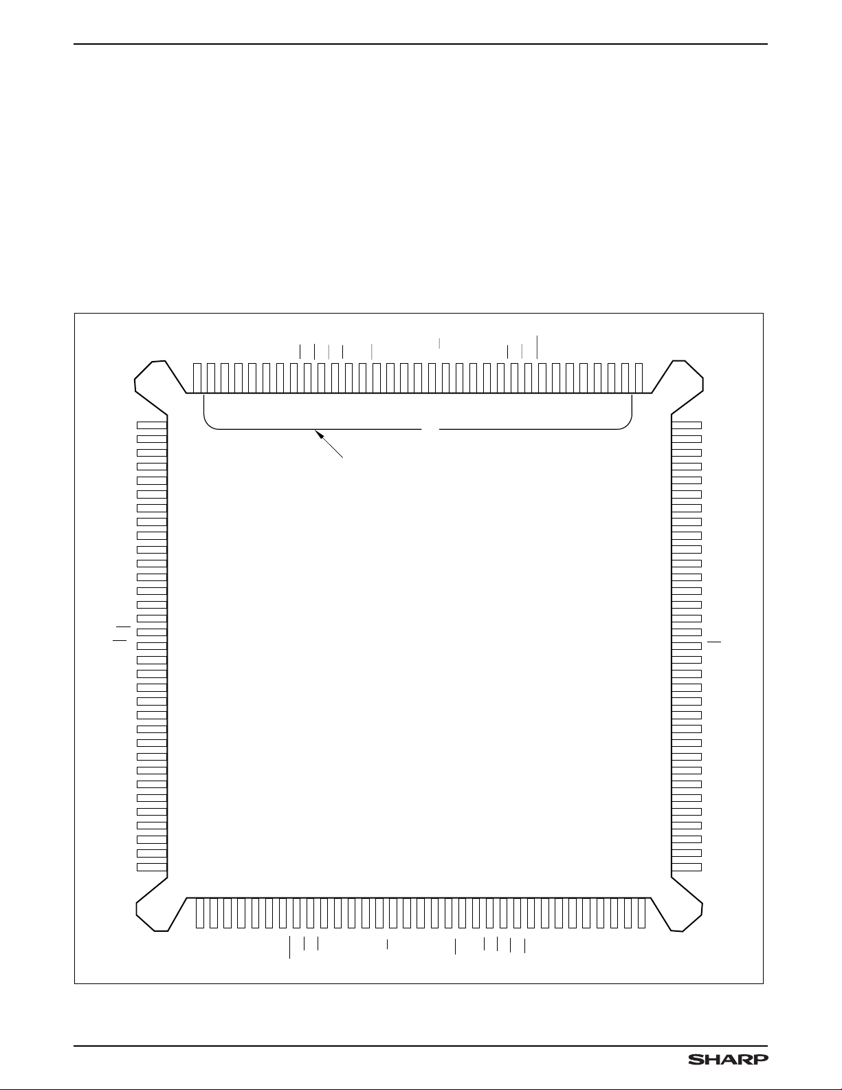
PIN CONNECTIONS
12AD13AD14A
11A
D
D
17
16151413121110
V
CCO
D
10A
D
9A
D
8A
V
SSO
D
7A
D
6A
D
5A
V
CCO
D
4A
D
3A
D
2A
V
SSO
D
1A
D
0A
RS
RT
1
D
0B
D
1B
D
2B
V
SSO
D
3B
D
4B
D
5B
V
CCO
D
6B
D
7B
D
8B
V
SSO
D
9B
D
10B
D
11B
V
CCO
18
19
20
21
22
23
24
25
26
27
28
29
30
31
32
33
34
35
36
37
38
39
40
41
42
43
44
45
46
47
48
49
50
SSO
V
D
A
15AD16AD17A
PF
9876543
HF1AF1FF1OE
CHAMFERED
EDGE
515253545556575859606162636465666768697071727374757677787980818283
A
CC
V
TOP VIEW
A2AA
tion or configuration information directly, to or from a
peripheral device on Port B, during sys te m star tup.
A word-width-select option is provided on Port B for
36-bit, 18-bit, or 9-bit data access. This feature allows
word- width matching between Por t A and Port B, with no
addit ion al logic n eeded. It a lso en sures maximum utilization of bus band widths .
A Byte Parity Check Flag at each port monitors data
integrity. Control-Register bit 0 ( zero) selects the parity
mode , odd or even. This bit is initialized for odd dat a parity
at reset; but i t may be reprogrammed for even parity, or
back a ga in to odd par it y , as des ired.
2
A
0A
1A
A
R/WAENAVSSACKAEF2MBF2D
CK
Pin 1
131
130
REQ
129
Pin 132
A
128
127
126
2
AE
125
124
18A
123
19A
D
122
SSO
V
121
20AD21AD22A
D
120
119
118
A
23
D
117
116
115
114
113
112
111
110
109
108
107
106
105
104
103
102
101
100
99
98
97
96
95
94
93
92
91
90
89
88
87
86
85
84
V
D
D
D
V
D
D
D
V
D
D
D
V
D
D
D
RT
V
D
D
V
D
D
D
V
D
D
D
V
D
D
D
V
CCO
24A
25A
26A
SSO
27A
28A
29A
CCO
30A
31A
32A
SSO
33A
34A
35A
2
SS
35B
34B
SSO
33B
32B
31B
CCO
30B
29B
28B
SSO
27B
26B
25B
CCO
12BD13BD14B
D
D
15B
SSO
V
16BD17B
D
1
MBF
1
AE
EF
1
B
ACK
B
B
REQ
EN
B
R/W
CK
SS
V
1
0
B
A
B
0B
WS
OE
WS
2
2
2
AF
HF
B
PF
D
18B
D
19B
D
20B
SSO
V
CC
FF
V
D
21B
D
22B
B
B
23
24
D
D
543601-30
Figure 1. Pin Connections f or 132-Pi n PQFP Package
(T op Vi ew )
2
Page 3
256 × 36 × 2 Bidirectional FIFO LH543601
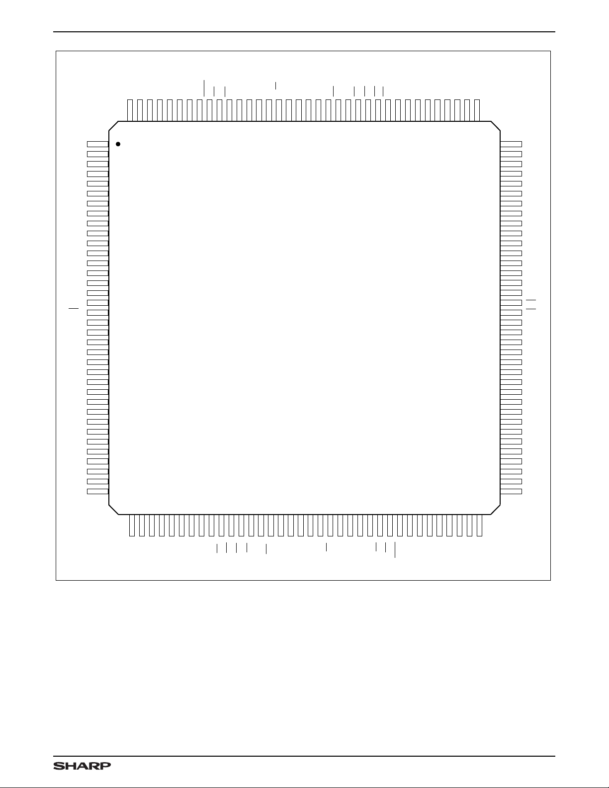
144-PIN TQFP
1
2
3
4
5
6
7
8
9
10
11
12
13
14
15
16
17
18
19
20
21
22
23
24
25
26
27
28
29
30
31
32
33
34
35
36
V
V
V
V
V
V
V
V
D
D
D
D
D
D
D
D
D
D
D
D
D
D
D
D
D
D
D
D
D
D
D
NC
CCO
24A
25A
26A
SSO
27A
28A
29A
CCO
30A
31A
32A
SSO
33A
34A
35A
RT
NC
V
35B
34B
SSO
33B
32B
31B
CCO
30B
29B
28B
SSO
27B
26B
25B
CCO
NC
2
SS
NC
144
23AD22AD21A
D
143
142
141
20A
D
140
SSO
V
139
19AD18A
D
138
137
MBF
136
2
SS
135
134
133
V
132
AE2EF2ACKAREQ
A
131
A
ENAR/W
130
129
A
CK
128
NC
127
0A
A
126
A1AA
125
2A
124
A
1
OEAVCCFF1HF1PF
123
122
121
AF
120
119
118
17A
D
117
16A
D
116
15A
D
115
SSO
V
114
14A
D
113
13A
D
112
12AD11A
D
111
110
TOP VIEW
NC
109
108
107
106
105
104
103
102
101
100
99
98
97
96
95
94
93
92
91
90
89
88
87
86
85
84
83
82
81
80
79
78
77
76
75
74
73
NC
V
D
D
D
V
D
D
D
V
D
D
D
V
D
D
RS
RT
NC
D
D
D
V
D
D
D
V
D
D
D
V
D
D
D
V
NC
CCO
10A
9A
8A
SSO
7A
6A
5A
CCO
4A
3A
2A
SSO
1A
0A
1
0B
1B
2B
SSO
3B
4B
5B
CCO
6B
7B
8B
SSO
9B
10B
11B
CCO
373839404142434445464748495051
NC
24BD23B
D
D
22B
D
21B
V
SSO
D
20B
19BD18B
D
PF
B
HF
AF
FF
CC
V
OE
2
2
2
Figure 2. Pin Connections for 144- Pin TQ FP Packa ge
53
54
52
1
0
B
NC
WS
WS
(T op Vi ew )
5556575859606162636465666768697071
1
1
B
B
B
R/W
EN
B
REQ
SS
V
0B
A
CK
B
ACK
EF
AE
1
MBF
D
17B
D
16B
V
SSO
D
15B
D
14B
13BD12B
D
72
NC
543601-38
3
Page 4

LH543601 256 × 36 × 2 Bidirect ional FIFO
PIN LIST
SIGNAL
NAME
A
0A
A
1A
A
2A
OE
A
FF
1
AF
1
HF
1
PF
A
D
17A
D
16A
D
15A
D
14A
D
13A
D
12A
D
11A
D
10A
D
9A
D
8A
D
7A
D
6A
D
5A
D
4A
D
3A
D
2A
D
1A
D
0A
RS 33 92
RT
1
D
0B
D
1B
D
2B
D
3B
D
4B
D
5B
D
6B
D
7B
D
8B
D
9B
D
10B
D
11B
D
12B
D
13B
D
14B
D
15B
PQFP
PIN NO.
1 126
2 125
3 124
4 123
6 121
7 120
8 119
9 118
10 117
11 116
12 115
14 113
15 112
16 111
17 110
19 106
20 105
21 104
23 102
24 101
25 100
27 98
28 97
29 96
31 94
32 93
34 91
35 89
36 88
37 87
39 85
40 84
41 83
43 81
44 80
45 79
47 77
48 76
49 75
51 71
52 70
53 69
54 68
TQFP
PIN NO.
SIGNAL
NAME
D
16B
D
17B
MBF
1
AE
1
EF
1
ACK
B
REQ
B
EN
B
R/
W
B
CK
B
A
0B
WS
0
WS
1
OE
B
FF
2
AF
2
HF
2
PF
B
D
18B
D
19B
D
20B
D
21B
D
22B
D
23B
D
24B
D
25B
D
26B
D
27B
D
28B
D
29B
D
30B
D
31B
D
32B
D
33B
D
34B
D
35B
RT
2
D
35A
D
34A
D
33A
D
32A
D
31A
D
30A
D
29A
PQFP
PIN NO.
56 66
57 65
58 64
59 63
60 62
61
63 59
64 58
65 57
66 56
67 55
68 53
69 52
70 51
72 49
73 48
74 47
75 46
76 45
77 44
78 43
80 41
81 40
82 39
83 38
85 34
86 33
87 32
89 30
90 29
91 28
93 26
94 25
95 24
97 22
98 21
100 18
101 17
102 16
103 15
105 13
106 12
107 11
109 9
TQFP
PIN NO.
61
SIGNAL
NAME
D
28A
D
27A
D
26A
D
25A
D
24A
D
23A
D
22A
D
21A
D
20A
D
19A
D
18A
MBF
2
AE
2
EF
2
ACK
A
REQ
A
EN
A
R/
W
A
CK
A
V
CC
V
SSO
PQFP
PIN NO.
PIN NO.
110 8
111 7
113 5
114 4
115 3
117 143
118 142
119 141
120 140
122 138
123 137
124 136
125 135
126 134
127 133
129 131
130 130
131 129
132 128
5 122
13 114
TQFP
NC 109
NC 108
V
V
V
V
CCO
SSO
CCO
SSO
18 107
22 103
26 99
30 95
NC 90
V
V
V
V
SSO
CCO
SSO
CCO
38 86
42 82
46 78
50 74
NC 73
NC 72
V
V
SSO
SS
55 67
62 60
NC 54
V
V
CC
SSO
71 50
79 42
NC 37
NC 36
V
V
V
CCO
SSO
CCO
84 35
88 31
92 27
NOTE:
PINS COMMENTS
V
V
CC
CCO
Supply internal logic. Connected to each other.
Supply output drivers only. Connected to each
other.
4
PINS COMMENTS
V
V
SS
SSO
Supply int erna l logic . Connec ted to each other .
Supply out put dri vers only. Connected to each
other .
Page 5
256 × 36 × 2 Bidirectional FIFO LH543601
RS
MBF
A
A
A
CK
R/W
EN
REQ
ACK
READ
WRITE
PORT B
I/O
PORT B
CONTROL
543601-36
PORT A
I/O
PORT A
CONTROL
WRITE
READ
FIFO 1
FIFO 2
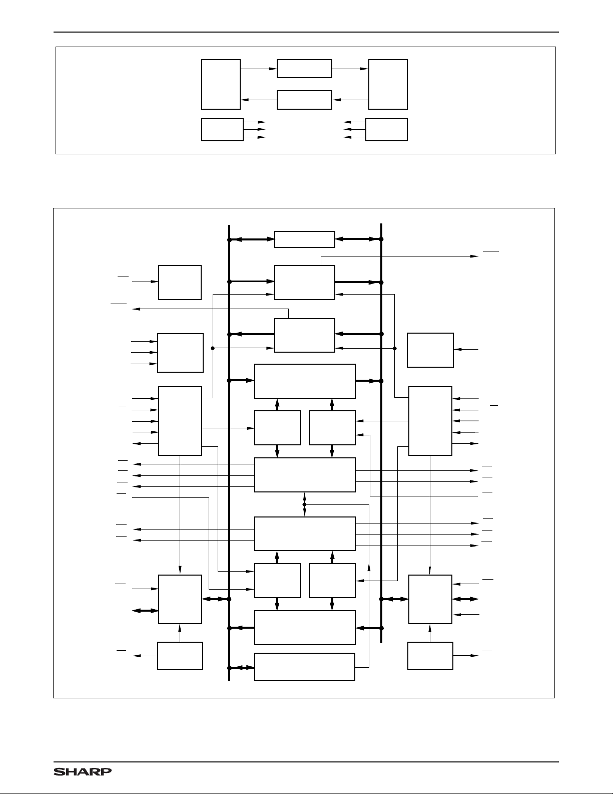
Figure 3a. Simplifie d LH543601 Bl ock Diag ram
BYPASS
MBF
1
RESET
LOGIC
2
2A
1A
0A
A
A
A
A
A
COMMAND
PORT AND
REGISTER
PORT A
SYNCH-
RONOUS
CONTROL
LOGIC
MAILBOX
REGISTER
#1
MAILBOX
REGISTER
#2
FIFO #1
MEMORY ARRAY
256 x 36
WRITE
POINTER
READ
POINTER
COMMAND
PORT AND
REGISTER
PORT B
SYNCH-
RONOUS
CONTROL
LOGIC
A
0B
CK
R/W
EN
REQ
ACK
B
B
B
B
B
D0A - D
FF
AF
HF
RT
EF
AE
OE
PF
35A
1
1
1
2
2
2
A
PORT A
I/O
FIXED AND
PROGRAMMABLE
STATUS FLAGS
FIXED AND
PROGRAMMABLE
STATUS FLAGS
READ
POINTER
FIFO #2
WRITE
POINTER
PORT B
I/O
EF
1
AE
1
RT
1
FF
2
AF
2
HF
2
OE
B
D0B - D
WS0, WS
35B
1
MEMORY ARRAY
256 x 36
A
PARITY
CHECKING
RESOURCE
PARITY
CHECKING
PF
B
REGISTERS
543601-6
Figur e 3b. Det aile d LH543601 Bl ock Diagr am
5
Page 6

LH543601 256 × 36 × 2 Bidirectional FIFO
PIN DESCRIPTIONS
PIN PIN TYPE
1
GENERAL
VCC, V
SS V
RS
I
Power, Ground
Reset
PORT A
CK
A
R/WA
EN
A I
A0A, A1A, A
OE
A
REQ
RT
2
D0A – D
FF
1
AF
1
HF
1 O
AE
2 O
EF
2
MBF
PF
A
ACK
2A I
A
35A
2
A
I
I
I
I
I
I/O/Z
O
O
O
O
O
O
Port A Free-Runn ing Clock
Port A Edg e-Sampled R ea d/ Write Contro l
Port A Edge-Sampled Enable
Port A Edge-Sampled Ad dres s Pins
Port A L evel- Sensit iv e Output Enable
Port A Request/Ena ble
FIFO #2 Retransmit
Port A Bidir ectional Dat a Bus
FIFO #1 Full Flag (Write Boundar y)
FIFO #1 Progra mmable Almo st-Fu ll Flag (Write Boundary)
FIFO #1 Half-Full Flag
FIFO #2 Program mable A lmost- Empty Flag (Read Boundar y)
FIFO #2 Empty Flag (Read Boundar y)
New-Mail-Alert Flag for Mailbox #2
Port A Parity Flag
Port A Acknowledge
PORT B
CK
B
R/W
B
EN
B
A
0B
OE
B
WS0, WS
REQ
RT
D0B – D
FF
AF
HF
AE
EF
MBF
PF
ACK
NOTE:
1. I = Input , O = O utput, Z = High-Impedance, V = Power Voltage Level
1
B
1
35B
2
2
2 O
1
1
1
B
B
I
I
I
I
I
I
I
I
I/O/Z
O
O
O
O
O
O
O
Port B Free-Run ning Clock
Port B Edge-Samp led Read/W rite Contro l
Port B Edge-Samp led Enable
Port B Edge-Sample d Address P in
Port B Level-Sensit ive Output Enable
Port B Word-Widt h Select
Port B Request / Enable
FIFO #1 Retransmit
Port B Bidirectional Data Bus
FIFO #2 Full Flag (Write Boundar y)
FIFO #2 Programm able A lmost-Full Flag ( Write Boundar y)
FIFO #2 Half-Full Flag
FIFO #1 Program mable A lmost- Empty Flag (Read Boundar y)
FIFO #1 Empty Flag (Read Boundar y)
New-Mail-Alert Flag for Mailbox #1
Port B Parity Flag
Port B Acknowled ge
DESCRIPTION
6
Page 7
256 × 36 × 2 Bidirectional FIFO LH543601
ABSOLUTE MAXIMUM RATINGS
PARAMETER RATING
1
Supply Voltage to VSS Pote n ti al –0.5 V to 7 V
Signal Pin Voltag e to VSS Potenti al
DC O utp ut C u rre nt
2
3
–0.5 V to VCC + 0 .5 V
± 40 mA
Stor age Tempera tur e Range –65oC to 150oC
Power Dissipat io n (Package Limit ) 2 Watt s (Quad Flat Pack)
NOTES:
1. Stresses greater than those listed under ‘A bsolute Maximum Ratings’ may cause
permanent damage to the device. This is a stress rating for transient conditions only.
Functional operation of the device at these or any other conditions outside those indicated
in the ‘Operating Range’ of this specification is not implied. Exposure to absolute maximum
rating conditions for extended periods may affect reliability.
2. Outputs should not be shorted f or more t han 30 seconds. No more than one output should be
shorted at any time.
3. Negat ive undershoot of 1.5 V in amplitude is permitted for up t o 10 ns, once per cycle.
OPERATING RANGE
SYMBOL PARAMETER MIN MAX UNIT
T
A
VCCSupply V olta ge
V
SS
V
IL
V
IH
NOTE:
1. Negat ive undershoot of 1.5 V in amplitude is permitted
for up to 10 ns, once per cycle.
Tem p erat ure,
Ambient
Supply V olta ge
Logic LOW
Input V olt age
Logic HIGH
Input V oltage
070
4.5 5.5 V
00V
–0.5 0.8 V
1
2.2
Vcc +
0.5
o
C
V
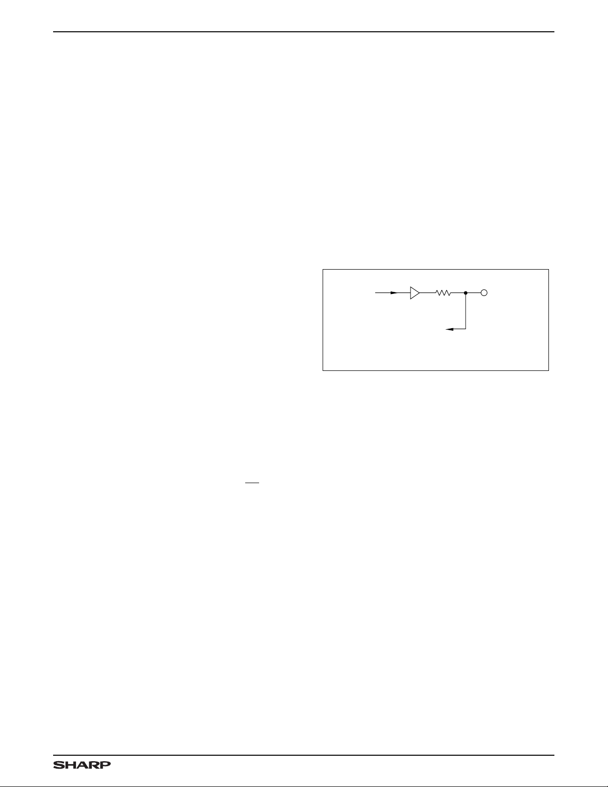
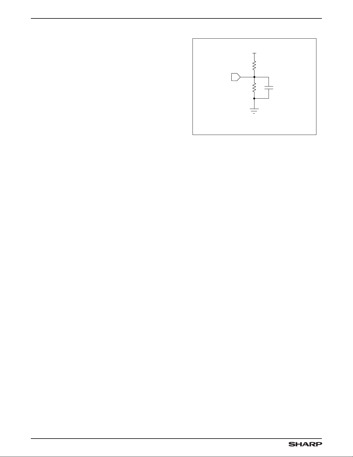
FROM PORT
INTERNAL
DATA BUS
(OR CONTROL
GATE)
IF ANY (SEE NOTE)
NOTE: Output-only pins have no
associated input buffer.
Figure 4. Struc tur e of Seri es Resis tor
15 Ω
TO ASSOCIATED
INPUT BUFFER,
Input/ Output Interface
D
nA/B
(OR FLAG)
543601-39
DC ELECTRICAL CHARACTERISTICS (Over Oper ating Range)
SYMBOL PARAMETER TEST CONDITIONS MIN TYP MAX UNIT
I
LI
I
LO
V
OL
V
OH
I
CC
I
CC2
I
CC3
I
CC4
NOTES :
1. ICC, I
with outputs open (for ICC: CL = 0 pF); and, for ICC and I
2. ICC (MAX.) using worst case conditions and data pattern. ICC (TYP.) using VCC = 5 V and and ‘average’ data pattern.
3. I
CC2
Inp ut Lea kage Cur re nt VCC = 5.5 V, VIN = 0 V T o V
I/O Leakage Current
OE ≥ VIH, 0 V ≤ V
OUT
≤ V
CC
CC
–10 10 µA
–10 10
Logic LO W Output V olt age IOL = 8 .0 mA
Logic HIG H Output Volt a ge IOH = –8.0 mA 2.4 V
Aver age Supply Cur rent
Aver age St andby Supply
Curr ent
1, 3
Po wer-Dow n S upply
Curr ent
1
Po wer-Dow n S upply
Curr ent
, I
CC2
CC 3
(TYP. ) and I
1, 3
, and I
are dependent upon actual output loading, and ICC and I
CC4
(TYP.) using VCC = 5 V and TA = 25°C.
CC4
1, 2
Measured at fCC = max
All Input s = V
(Clocks idle)
IHMIN
All Input s = VCC – 0.2 V (Clo cks idle)
All Input s = VCC – 0. 2 V
(Clocks at fcc = max)
are also dependent on cycle rates. Specified values are
, operating at minimum cycle times.
CC4
CC4
180 280 mA
13 25 mA
0.002 0.4 mA
610mA
0.4 V
µA
7
Page 8
LH543601 256 × 36 × 2 Bidirectional FIFO
AC TEST CO NDI T IO N S
PARAMETER RATING
470 Ω
240 Ω
+5 V
30 pF
*
Input Pulse Levels
Input Rise and Fall Times
(10% to 90%)
Output Refer ence Le vels
Input T iming Ref ere nce Lev els
VSS to 3 V
5 ns
1.5 V
1.5 V
DEVICE
UNDER
TEST
Output L oad, Timing Tests
CAP ACIT ANCE
1,2
PARAME TER RAT ING
CIN (Input Capacitance)
C
(Output Ca pacit ance)
OUT
NOTES:
1. Sample tested only.
2. Capacitances are maximum values at 25oC, measured at 1.0MHz,
with VIN = 0 V.
Figure 5
8 pF
8 pF
*
INCLUDES JIG AND SCOPE CAPACITANCES
Figur e 5. Outp ut Load Circui t
543601-7
8
Page 9

256 × 36 × 2 Bidirectional FIFO LH543601
AC ELECTRICAL CHARACTERISTICS 1 (VCC = 5 V ± 10%, TA = 0°C to 70°C)
SYMBOL DECRIPTION
f
CC
t
CC
t
CH
t
CL
t
DS
t
DH
t
ES
t
EH
t
RWS
t
RWH
t
RQS
t
RQH
t
AS
t
AH
t
A
t
ACK
t
OH
t
ZX
t
XZ
t
EF
t
FF
t
HF
t
AE
t
AF
t
MBF
t
PF
t
RS
t
RSS
t
RSH
t
RF
t
FRL
t
FWL
t
BS
t
BH
t
BA
NOTES:
1. Timing measurements performed at ‘AC Test Condition’ levels.
2. Values are guaranteed by design; not currently production tested.
3. t
RSS
ENB is being asserted.
4. t
FRL
5. t
FWL
Clock Cycle Frequency — 50 — 40 — 33 — 28.5 MHz
Clock Cycl e Ti me 20 — 25 — 30 — 35 — ns
Clock HIGH Ti me 8 — 10 — 12 — 15 — ns
Clock LOW T im e 8 — 10 — 12 — 15 — ns
Data Setup Time 10 — 12 — 13 — 15 — ns
Data Hold Time 0—0—0—0—ns
Enable Set up T ime
Enable Hol d T ime 0—0—0—0—ns
Read/W ri te Setu p Ti me 10.4 — 13 — 15 — 18 — ns
Read/W ri te Hold Tim e 0—0—0—0—ns
Request Setup Time 12 — 15 — 18 — 21 — ns
Request Hold Time 0—0—0—0—ns
Address Setup Time
Address Hold Time
6
6
Data Out put Access Ti me — 12.8 — 16 — 20 — 25 ns
Acknowl edge Acce ss T im e — 12 — 15 — 20 — 25 ns
Output Hold Time 2.0 — 2.0 — 2.0 — 2.0 — ns
Output Enable Time, OE LOW to D
– D35 Low-Z
Output Disable Time, OE HIGH to
– D35 High-Z
D
0
2
2
0
Clock to EF Flag V a lid (Em pty Fla g) — 17.6 — 22 — 25 — 30 ns
Clock to FF Flag V a lid (Fu ll Flag ) — 17.6 — 22 — 25 — 30 ns
Clock to HF Flag V a lid (Ha lf- Full ) — 17.6 — 22 — 25 — 30 ns
Clock to AE Flag Valid (Almost-
Empty)
Clock to AF Flag V a lid (Al most -Fu ll) — 16 — 20 — 25 — 30 ns
Clock to MBF Flag V alid (Mail box
Flag)
Data to Parity Flag Valid — 13.6 — 17 — 20 — 25 ns
Reset/ Retr ansm it Puls e Width
Reset/ Retr ansm it Set up T ime
Reset/ Retr ansm it Hol d Ti me
7
3
3
Reset LOW to Flag V ali d — 28 — 35 — 40 — 45 ns
First Read Latenc y
First Wr ite Latency
4
5
Bypass Data Setup 12 — 15 — 18 — 21 — ns
Bypass Data Hold 3—5—5—5—ns
Bypass Da ta Ac cess — 18 — 20 — 25 — 30 ns
and/or t
is the minimum first-write-to-first-read delay, following an empty condition, which is required to assure valid read data.
is the minimum first-read-to-first-write delay, following a full condtion, which is required to assure successful writing of data.
need not be met unless a rising edge of CKA occurs while ENA is being asserted, or else a rising edge of CKB occurs while
RSH
–20 –25 –30 –35
MIN MAX MIN MAX MIN MAX MIN MAX
10.4 — 13 — 15 — 15 — ns
12—15—18—21—ns
0—0—0—0—ns
1.5 — 2.0 — 3.0 — 3.0 — ns
— 9 —12—15—20ns
—16—20—25—30ns
—12—15—20—25ns
32/20 — 40/25 — 52/30 — 65/35 — ns
16—20—25—30—ns
8 —10—15—20—ns
20—25—30—35—ns
20—25—30—35—ns
UNITS
9
Page 10

LH543601 256 × 36 × 2 Bidirectional FIFO
OPERATIONAL DESCRI PT ION
Reset
The device is r eset wh enever the a synchro nous Res et
(RS) in put is taken LOW , and at leas t one rising edge an d
one falling edge of both CKA and CKB occur while RS is
LOW . A reset ope ration is r equired af ter power-u p, before
the f irst wr it e operat ion ma y occur. The LH543601 is fu lly
ready for ope ration afte r being reset . No device progra mming is required if the default states described below are
accepta ble.
A reset operation initializes the read-address and
write-a ddr ess p o inter s for FIFO #1 and FIFO #2 to t hose
FIFO’s first physical memory locations. If the respective
outputs are enabled, the initial contents of these first
locations appea r at the outputs. FIFO and mailbo x status
flags are updated to indicate an empty condition. In
addition, the progr am mab le-stat us -flag of fset values are
initialized to eight. Thus, the AE1/AE2 flags get asserted
within eight locations of an empty condition, and the
AF1/AF2 flag s likewise ge t asserted with in eight locations
of a full condition, for FIFO #1/FIFO #2 respectively.
Bypass Operation
During reset (whenever RS is LOW) the device acts
as a registered transceiver, bypassing the internal FIFO
memories. Port A acts as the m aster port. A write or read
operat ion on Port A during r ese t transf er s data dire ctly to
or from Port B. Port B is considered to be the slave, and
cannot perform write or read operations indepen dently on
its own during reset .
The direction of the bypass data trans mission is determined by th R/WA control input, which does not get
overridden by the RS input. Here, a ‘write’ operation
means passing data from Port A to Port B, and a ‘read’
operat ion me ans pas sing data f rom Por t B to Port A.
The bypass capability may be used to pass initialization or configur ation data directly bet ween a master processor and a peripher al device du ring r eset .
(CKA or CKB) whenever: the appropriat e e na ble (ENA or
ENB) is held HI GH; the appropriate request (RE QA or
REQB) is held HIGH; the appr opr iat e Read/ Wr ite contro l
(R/WA or R/WB) is held LOW; the FIFO address is
selected for the address inputs (A2A – A0A or A0B); and
the prescribed setup times and hold time s are observ ed
for all of these signals. Set up tim es and hold times mus t
also be observed on the data-bus pins (D0A – D
D0B – D
35B
).
35A
or
Normally, the appropriate Output Enable signal (OE
or OEB) is HIGH, to disable the outputs a t that port, so
that the data word present on the bus from external
sources gets stored. However, a ‘loopback’ mode of
operation also is possible, in which the data word supplied
by the outputs of one internal FIFO is ‘turned around’ at
the port and r ead ba ck int o the ot her FIFO. In this mode ,
the outputs at the port are not disabled. To remain within
specification for all timing parameters , the Clock Cycle
Frequency must be reduced slightly below the value
which otherwise would be permissible for that speed
grade of LH543601.
When a FIFO full condition is r eached, write operat ions
are locked out. Following the first read operation from a
full FIFO, another memory location is freed up, and the
cor responding Full Flag is deasserted (FF = HIGH ). The
first write operation should begin no earlier than a First
Write Latency (t
) after the first read operation from a
FWL
full FIFO, to ensure that correct read data are retrieve d.
FI FO Rea d
Po rt A r eads from FIFO #2, and Por t B reads from FIFO
#1. A read operation is initiated on the rising edge of
a clock (CKA or CKB) whenever: the appropriate enable
(ENA or ENB) is held HIGH; the appropriate request
(REQA or REQB) is held HIGH; the appropriate
Read/Write control (R/WA or R/WB) is held HIGH;
the FIFO address is selected for the address inputs
(A2A – A0A or A0B); and the prescribed setup times and
hold t imes are obse rved for all of these signals. Read data
A
Address Modes
Address pins select the device resource to be
accessed by each port. Port A has three resource -register-select inputs, A0A, A1A, and A2A, which s elect be tween
FIFO access, mailbox-register access, control-register
access (writ e only) , and p rogramm able flag- of fset -valueregister access. Port B has a single address input, A0B,
to select between FIFO access or mail box-register access.
The status of the resource-register-select inputs is
sampled at the rising edge of an enabled clock (CKA or
CKB). Resource- regist er select-input address definitions
are summarized in Table 1.
FIFO Write
Port A writ es to FIFO #1, and Por t B writes to FIFO #2.
A write operation is initiated on the rising edge of a clock
10
T abl e 1. Resource-Regi ste r Addresses
A2AA1AA
0A
HHH
HHL
HLH
HLL
LHH
LHL
LLH
FIFO
Mailbox
AF2, AE2, AF1, AE1 Flag Offsets
Register (36-Bit Mode)
Contro l Register (Par ity M ode)
AE1 Flag Offset Register
AF1 Flag Of fset Register
AE2 Flag Offset Register
RESOURCE
PORT A
LLLAF2 Flag Of fset Register
A
0B
H
L
FIFO
Mailbox
RESOURCE
PORT B
Page 11

256 × 36 × 2 Bidirectional FIFO LH543601
OPE RATIO N AL D ESCRIPT IO N (cont’d)
becomes valid on the data-bus pins (D0A – D
D0B – D
) by a time tA after the rising clock (C KA or
35B
CKB) edge, provided that the data outputs ar e enabled.
OEA and OEB are as sertiv e-LOW , asy nchr onous, O utput Enable control input signals. Their effect is only to
enable or disable t he outp ut driv ers of th e respec tive por t.
Disabling the out puts does
not
disable a read operation;
data trans mitt ed to the corres ponding o utp ut register wi ll
remain available later, when the outputs again are enabled, unless it subsequent ly is over written .
When an empty condition is reached, r ead operat io ns
are locked out until a valid write operation(s) has loaded
additional data into the FIFO. Following the first wri te to
an empty FIFO, the corresponding empty flag (EF) will be
deasser ted (HIGH). The first read oper ation should begin
no earlier than a First Read Latency (t
) after the first
FRL
write to an empty FIFO , to ensure th at corr ect read data
words are retrieved.
Dedicated FIFO Status Flags
Six dedicated FIFO status flags are i ncluded for Full
(FF1 and FF2), Half-Ful l (HF1 and HF2), and Empty (EF
and EF2). FF1, HF1, and EF1 indicate the status of FIFO
#1; and FF2, HF2, and EF2 ind icate the sta tus of FIFO #2.
A Full Flag is asser ted following the first subsequent
rising clock edge f or a write oper ation which fills the FIFO.
A Full Flag is deasserted following the first subsequent
falling clock edge for a read operation to a full FIFO. A
Half-Full Flag is updated following the first subsequent
rising clock edge of a read or w rite operation to a FIF O
which changes its ‘half-full’ status. An Empty Flag is
asserted following the firs t subsequent rising clock edge
for a read operation which empties the FIFO. An Empty
Flag is deasserted following the falling clock edge for a
write oper atio n to an empty FIFO.
Programmable Status Fla gs
Four programmable FIFO s tatus flags are provided,
two for Almost-Full (AF1 and AF2), and two for AlmostEmpty ( AE1 and AE2). Th us, each p ort has t wo programmable flags t o mon itor the st atus of t he two int ernal FIFO
buffer memories. The offset values for these flags are
initialized to eight locations from the respective FIFO
boundaries during reset , but can be reprog ram med over
the e nt ir e FI FO d e pth.
An Almost-Full Flag is asserted following the first su bsequent rising clock edge after a write operation which
has partiall y fill ed th e FIF O up to th e ‘almost-full’ offset
point. An Almost-Full F lag is deasser ted following the first
subsequent falling clock edge after a read operation
which has partially emptied the FIFO down past the
‘almost-full’ offset point. An Almost-Empty Flag is asserted following the first subsequent rising clock edge
after a read operation w hich has partially emptied the
FIFO down to the ‘almost-empty’ offs et point. An AlmostEmpty Flag is deasserted following the first subsequent
35A
or
fall ing clock edge after a write operation which has partially filled the FIFO up past the ‘almost-empty’ offset
point.
Flag off se ts may be written or r ead thr ough the Por t A
data bus. Al l four program mable FI FO status flag of fset s
can be set simultaneously through a single 36-bit status
word; or, each programmable flag offset can be set
individually, through one of four eight-bit status words.
Table 3 illustrates the data format for flag-programming
words .
Also, Table 4 defines the meaning of each of the five
flags, both the dedicated flags and the programmable
flags, for the LH543601.
WARNING: Contro l inputs which may affec t the com putation of flag values at a port generally should not change
while the clock for that port is HIGH, since some updatin g
of flag values takes place o n t he
falling
edge of t he clock.
Mailbox Operation
Two mailbox registe rs are pr ovided f or pass ing system
hardwar e or software control/ status words between ports.
Each port can read its own mailbox and write to the other
1
port’s mailbox . Mailbox access is p erf or me d on the rising
edge of the controlling FIFO’s clock, with the mailbox
address selected and the enable (ENA or ENB) H IGH.
That is, writing to Mailbox Register #1, or reading from
Mai lbox Register #2, is synch ron ized to C KA; and writin g
to Ma ilbox Regist er #2, or reading f rom M ailbox Regist er
#1, is synch ronized to CKB.
The R/W
and OE
A/B
pins control the direction and
A/B
availabi lity of mailbox-registe r accesses. Each mailbox
register has its own New-Mail-Alert Flag (MBF1 and
MBF2), which is synchronized to the reading port’s clock .
These New-Mail -Alert Flags are s tatus indicators only,
and cannot inhibit mailbox-register read or write operations.
Request Acknowledge Handshake
A sync hro nous reque st-ac knowledge ha ndsha ke feature is provided for each port, to perform boundary synchronization between asynchronously-operated ports.
The use of this feature is optional. When it is used, the
Request input (REQ
With REQ
HIGH, R/W
A/B
) is sampled at a rising clock edge.
A/B
dete rmines whether a FI FO
A/B
read operation or a FIFO write operation is being requested. The Acknowledge output (ACK
A/B
during the following clock cycle(s). ACK
setup and hold time requirements of the Enable input
(ENA or E NB). There fore, ACK
may be tied back to the
A/B
enable input to directly gate FIFO accesses, at a sl ight
decrea se in maxim um oper ating frequenc y.
The assertion of ACK
asserted. However, ACK
EN
; and thus the assert ion of ACK
A/B
signifies that REQ
A/B
does not depen d logically on
A/B
does
A/B
that a FIFO write access or a FIFO read access act ually
took place. While REQ
HIGH, ACK
may be considered as a synchronous,
A/B
predictive boundary flag. That is, ACK
and EN
A/B
are being held
A/B
A/B
) is updated
meets the
A/B
was
A/B
not
prove
acts as a syn-
11
Page 12

LH543601 256 × 36 × 2 Bidirectional FIFO
OPE RATIO N AL D ESCRIPT IO N (cont’d)
chronized predictor of the Almost-Full Flag AF for write
operat ions, or as a sy nchronized pr edictor of the AlmostEmpty Flag A E for re ad operatio ns.
Outside the ‘almost-full’ region and the ‘almo s t-em pty ’
region, ACK
REQ
is he ld cont inuously HIGH. With in t he ‘alm ost-full’
A/B
region or the ‘almost-empty’ region, ACK
on every
actual full or empty boundaries and to ensure that the t
(first write lat ency ) an d t
tions are sat isf ied befor e AC K
The ‘almost-full region’ is defined as ‘that region, where
the Almost-Full Flag is being asserted’; and the ‘almostempty region’ as ‘that region, where the Almost-Empty
Flag is being asserted. ’ Thus, t he extent of these ‘almost’
regions depends on ho w the system h as p rog ramm ed the
offset values for the Almost-Full Flags and the AlmostEmpty Flags . If the system has
then these offset values remai n at their default values,
eight in each case.
If a write attempt is unsuccessful because the correspond ing FI FO is full, or if a r ead atte mpt is unsucces sf u l
because th e corresp onding FIFO is empty , ACK
asserted in respons e to REQ
If the REQ/ACK handshake is not used, then the
REQ
input may be used as a second enable input, at
A/B
a possible mino r loss in maximum operating speed. In this
case, the ACK
WARNING : Whether or not the REQ/A CK handshake is
being used, the REQ
for that port to function at all – for FIFO, mailbox, or
data- bypas s operat ion.
Data Retransmit
A retransmit operation resets the read-address pointer of
the c orre spo nding FIF O (#1 or # 2) bac k to the fi rs t FIFO
physical memory location, so that data may be reread. The
write pointer is not aff ected. The sta tus flags are updated;
and a block of up to 256 data words, which previously had
been writt en i nto and read fr om a FIFO, can be retrieved.
The block to be retransmitted is bounded by the first FIFO
memory location, and the FIFO memory location addressed
by the write pointer. FIFO #1 retransmit is initiated by
strobing the RT1 pin LOW. FIFO #2 retransmit is initiated by
strobing the RT2 pin LOW. Read and write operations to a
FIFO should be stopped while the corresponding Retransmit signal is being asserted.
Parity Checki ng
The Parity Check Flags, PFA and PFB, are asserted
(LOW) whenever there is a parity error in the data word
present on the Port A data bus or the Port B data bus
respectively. The inputs to the parity-evaluation logic
come direct ly (via is o lation trans is tors) fr om th e data-bus
bonding
remains continuously HIGH whenever
A/B
occurs only
A/B
third
cycle, to prevent an overrun of the FIFO’s
(first read late ncy) specific a-
FRL
is received.
A/B
not
programmed them,
.
A/B
output may be ignored.
A/B
input for a port
A/B
pads
, in each case. Thus, PFA and PFB provide
must
be asserted
A/B
is
FWL
not
parity-error indications for whatever 36-bit words are
present at Port A and Port B respectively, regardless of
whether those words originated within the LH543601 or
in the external system.
The four bytes of a 36-bit data word are grouped as D0 –
D8, D9 – D17, D18 – D26, and D27 – D35. The parity of each
nine-bit byte is individually checked, and the four single-bit
parity indications are logically inclusive-ORed and inverted,
to produce the Parity-Flag output. Parity checking is initialized for odd parity at reset, but can be reprogrammed fo r
ev en par it y or for odd par ity dur ing o per atio n. Control- Register bit 00 (zero) selects the parity mode, odd or even.
(See Table 3.)
All nine bits of each byte are treated alike by the parity
log ic. The byte parit y ove r the nine bit s is compar ed w ith
the Parit y Mod e bit in the Cont r ol Reg iste r , to gene rate a
byt e-parity- error indication. Then, the four byte-parityerr or signals a re NORed t oget her, to comput e the a sser tive- LOW parity -flag value.
Word-Width Selection on Port B
The word width of data access on Port B is selected
by the WS0 and WS1 contr ol input s. WS0 and WS1 both
are tied HIGH for 36-bit access; they both are tied LOW
for single-byte access. For double-byte access, WS0 is
tied HI GH and WS1 is tied LOW . (See Table 2.)
In the single-byte-access or double-byte-access modes,
FIFO w rite operations on Port B e ssentially pack the data to
form 36-bit words, as viewed from Port A. Similarly, singlebyte or double -byte FI FO read opera tions o n Po rt B e ssentially unpack 36-bit words through a series of shift
opera tions . FI FO status flags are u pdated fo llow ing th e la st
access which forms a complete 36-bit transfer.
Sin ce the valu es for eac h st atu s fl ag a re co mpute d by
logic directly associated with one of the two FIFO-memory
array s, and not by l ogic a ssoci ated w ith P ort B,
the flag
values reflect the arra y fullness situation in term s of c omplete 36-bit words
, and no t in terms of bytes or double byte s.
However , there is no such re strict ion for switc hing from
writing t o reading, or from r eading to writing, at Port B. A s
long as t
state after
, tDS, and tA are sat isfied, R/ WB may ch ange
RW S
any
single- byte or doub le-byte access, and not
only aft er a full 36- bit- wor d access.
Also, the word-width-matching feature continues to
oper at e prop erly in ‘ loopback ’ mode.
Note that the program mable word-width-matching feature is
Data Bypass operations do
only
supported fo r FIFO accesses. Mailbox and
not
support word-width
matching between Port A and Port B. Tables 2, 3, and 4,
and Figures 6a, 6b, 7a, and 7b summarize word-width
select ion fo r Port B.
Tab le 2. Port B Word-W idt h Sel ection
WS
1
H H 36-B it
H L (Reserved)
L H 18-Bit
L L 9-Bit
WS
0
PORT B DATA WIDTH
12
Page 13

256 × 36 × 2 Bidirectional FIFO LH543601
Table 3. Resourc e-Register Programming
RESOURCE-
REGISTER
ADDRESS
A2AA1AA
0A
RESOURCE-REGISTER CONTENTS
NORMAL FIFO OPERATION
D
35A
D
0A
HHHX... ...X
MAILBOX
D
35A
D
0A
HHLX... ...X
AF2, AE2, AF1, AE1 FLAG OFFSETS REGISTER (36-BIT MODE)
D
D
35A
34A
. . . D
HLHX AF2 Offset
D
35A
H L L X... ...X Parity Mode
27A
D
26A
1
X AE2 Offset
D
25A
. . . D
18A
D
17A
1
X AF1 Offset
D
. . . D
16A
CONTROL REGISTER: (WRITE-ONLY) PARITY EVEN/ODD
8-BIT AE1 FLAG OFFSET REGISTER
9A
D
8A
1
X AE1 Offset
D
D7A . . . D
1A
0A
1
D0A
2
D
35A
D
8A
D7A . . . D
LHHX... ...X AE1 Offset
AF1 FLAG OFFSET REGISTER
8-BIT
D
35A
D
8A
D7A . . . D
LHLX... ...X AF1 Offset
8-BIT AE2 FLAG OFFSET REGISTER
D
35A
D
8A
D7A . . . D
LLHX... ...X AE2 Offset
AF2 FLAG OFFSET REGISTER
8-BIT
D
35A
D
8A
D7A . . . D
L L L X... ...X AF2 Offset
NOTES:
1. All four programmable-flag-offset values are initialized to eight (8) during a reset operation.
2. Odd parity = HIGH; even parity = LOW. The parity m ode is initialized t o odd during a res e t operation.
0A
1
0A
1
0A
1
0A
1
13
Page 14

LH543601 256 × 36 × 2 Bidirectional FIFO
1
FLAG
Table 4. Flag Definition Table
VALID REA D CYCLES REMAINING VALID WRITE CYCLES REMAINING
FLAG = LOW FLAG = HIGH FLAG = LOW FLAG = HIGH
MIN MAX MIN MAX MIN MAX MIN MAX
FF 256 256 0 255 0 0 1 256
AF 256-p 256 0 255-p 0 p p + 1 256
HF 129 256 0 128 0 127 128 256
AE 0 q q + 1 256 25 6-q 256 0 255-q
EF 0 0 1 256 256 256 0 255
NOTES:
1. q = Programmable-Almost-Empty Offset value. (Default value: q = 8.)
2. p = Programmable-Almost-Full Offset value. (Default value: p = 8.)
14
Page 15

256 × 36 × 2 Bidirectional FIFO LH543601
PORT B WORD-W IDT H S ELE CTI ON
18-Bit Data Streams36-Bit Data Stream
Bits 18-35
(2nd Halfword)
Bits 0-17
(1st Halfword)
Bits 0-17
(1st Halfword)
18
18
D
35B
2nd Halfword, then 1st Halfword
D
18B
PORT
B
D
17B
1st Halfword, then 2nd Halfword
D
0B
543601-32
PORT
A
D
35A
18
Bits 18-35
(2nd Halfword)
D
18A
D
17A
18
D
0A
Figur e 6a. 36- to-1 8 Funnel ing Through FI FO #1
PORT
A
9-Bit Data Streams36-Bit Data Stream
D
35A
9
D
27A
D
26A
9
D
18A
Bits 27-35
(4th Byte)
Bits 18-26
(3rd Byte)
D
35B
9
D
27B
D
26B
9
D
18B
4th Byte, then 1st Byte, then 2nd Byte, then 3rd Byte
3rd Byte, then 4th Byte, then 1st Byte, then 2nd Byte
PORT
D
17A
9
D
9A
D
8A
9
D
0A
Bits 9-17
(2nd Byte)
Bits 0-8
(1st Byte)
D
17B
9
D
9B
D
8B
9
D
0B
B
2nd Byte, then 3rd Byte, then 4th Byte, then 1st Byte
1st Byte, then 2nd Byte, then 3rd Byte, then 4th Byte
543601-34
Figur e 6b. 3 6-to- 9 Funnel ing Through FIFO #1
NOTES:
1. The heavy black borders on register segments indicate the main
data path, suitable for most applications. Alternate paths feature
a different ordering of bytes within a word, at Port B.
2. The fu nneling process does not change the ordering of bits within
a byte. Half words ( Figure 6a) or bytes (Fig ure 6b) are transferred in parallel form from Port A to Port B.
3. The word-width setting may be changed during system operation;
howev er, two clock intervals should be allowed for these signals
to settle, before again attempting to read D
dummy w ords should be passed through initially. Also, incom-
– D
0B
, and three
35B
plete data words may occur, when the word width is changed
from shorter to longer at an inappropriat e point in t he data block
passing through the FIFO.
15
Page 16

LH543601 256 × 36 × 2 Bidirectional FIFO
PORT B WORD-WIDTH SELECTIO N
18-Bit Data Stream36-Bit Data Stream
PORT
A
PORT
A
D
D
D
D
D
35A
27A
26A
18A
17A
9
9
9
D
35A
D
18A
D
17A
D
0A
18
18
Bits 27-35
(4th Byte)
Bits 18-26
(3rd Byte)
Bits 9-17
(2nd Byte)
D
35B
Bits 18-35
18
(2nd Halfword)
D
18B
PORT
B
D
17B
1st Halfword, then 2nd Halfword
Bits 0-17
(1st Halfword)
18
D
0B
Figure 7a. 18-to-36 Defunneling Through FIFO #2
9-Bit Data Stream36-Bit Data Stream
D
35B
9
D
27B
D
26B
9
D
18B
PORT
D
17B
9
B
543601-33
D
9A
D
8A
Bits 0-8
9
(1st Byte)
D
0A
Figur e 7b. 9- to-3 6 Defunnel ing Thr ough FIFO #2
NOTES:
1. The heavy black borders on register segments indicate the only
data paths used. The other byte segments of Port B do not participate in the data path during defunneling.
2. The defunneling process does not change the ordering of bits
within a byte. Halfwords (Figure 7a) or bytes (Figure 7b) are
transferred in parallel form from Port B t o Port A.
16
D
9B
D
8B
9
D
0B
1st Byte, then 2nd Byte, then 3rd Byte, then 4th Byte
543601-35
3. The word-width setting may be changed during system operation;
however, two clock intervals should be allowed for these signals
to settle, before aga in attempting to send data, and three
dummy words should be passed through initia lly. Also, incomplete data words may occur, when the word width is changed
from short er to longer at an inappropriate point in the data block
passing through the FIFO.
Page 17

256 × 36 × 2 Bidirectional FIFO LH543601
TIMING DIAGRAMS
t
RS
RS
CK
EN
REQ
CK
EN
t
RSS
A
t
A
t
RQStRQH
A
t
RSS
B
t
B
t
RQStRQH
t
ES
ES
EH
t
EH
t
t
RSH
RSH
t
RSS
t
ES
t
RQStRQH
t
RSS
t
ES
t
RQStRQH
t
EH
t
EH
REQ
B
t
RF
EF, AE
t
RF
HF, AF, FF, MBF
NOTES:
1. RS overrides all other input signals, except for R/W
asynchronously. RS operates whether or not ENA and/or ENB are asserted. However,
, ENA, and REQA. It operates
A
at least one rising edge and one falling edge of both CKA and CKB must occur while
RS is being asserted (is LOW), with timing as defined by t
2. Otherwise, t
occurs while that clock is enabled.
RSS
, t
need not be met unless the rising edge of CKA and/or CK
RSH
RSS
and t
RSH
.
B
3. The parity-check even/odd selection (Control Register bit 00) is initialized to odd byte
parity at reset (HIGH).
4. The AE and AF flag offsets are initialized to eight locations from the boundary at reset.
Figure 8. Re s et Tim in g
543601-26
17
Page 18

LH543601 256 × 36 × 2 Bidirectional FIFO
TIMING DI AGRAMS (cont ’d)
RS
CK
R/W
EN
REQ
OE
t
RSS
A
RWS
ES
RQS
t
BS
t
RWH
t
t
t
EH
RQH
BH
t
t
A
t
A
t
A
B
t
RWS
t
t
A
ZX
t
RWH
t
RQStRQH
t
ES
EH
t
BA
t
OH
t
RSH
D0B - D
D0A - D
35B
OE
35A
A
BYPASS IN
PREVIOUS DATA
t
BA
t
OH
BYPASS
OUT
NOTES:
, t
1. t
RSS
need not be met unless the rising edge of CKA or CKB occurs while that clock is enabled.
RSH
2. Port A is considered the master port for bypass operation. Thus, CK
the transmission of data between ports at reset.
Figure 9. Dat a Bypass Timin g
BYPASS DATA OUT
t
t
BH
BS
t
XZ
BYPASS
IN
, R/WA, ENA, and REQA control
A
543601-27
18
Page 19

256 × 36 × 2 Bidirectional FIFO LH543601
TIMING DI AGRAMS (cont ’d)
CK
R/W
EN
REQ
A
READ FROM
FIFO #2
t
CH
A
t
A
A
t
A
2A
t
RWS
t
RQStRQH
t
RWH
t
ES
AS
EH
t
AH
t
CC
t
CL
WRITE TO
FIFO #1
t
t
RWS
t
t
RQStRQH
t
RWH
t
ES
AS
EH
t
AH
A
1A
A
0A
OE
A
t
A
t
ZX
D0A - D
35A
PF
A
NOTES:
1. The Port A Parity Error Flag (PF
2. The status of OE
3. If OE
is left LOW during a write operation, then the previous data held in the output latch is
A
does not gate read or write operations.
A
written back into FIFO #1.
t
t
PREVIOUS
t
PF
) reflects the parity status of data present on the data bus.
A
t
AS
AS
AH
t
AH
t
A
t
OH
DATA
t
VALID PF VALID PF VALID PF
DATA OUT
PF
t
XZ
t
t
t
t
PF
AS
AS
DS
DATA IN
t
AH
t
AH
t
DH
543601-24
Figure 10. Port A FIFO Read/W rite
19
Page 20

LH543601 256 × 36 × 2 Bidirectional FIFO
TIMING DI AGRAMS (cont ’d)
CK
R/W
EN
REQ
READ FROM
FIFO #1
t
B
RWS
t
t
RQS
t
AS
t
RWH
t
t
t
EH
RQH
AH
ES
t
B
B
B
A
0B
CH
t
CC
t
CL
WRITE TO
FIFO #2
t
RWS
t
ES
t
RQS
t
AS
t
RWH
t
t
RQH
t
AH
EH
OE
B
t
D0B - D
35B
PF
B
NOTES:
1. The Port B Parity Error Flag (PF
2. The status of OE
3. If OE
is left LOW during a write operation, then the previous data held in the output latch is
B
does not gate read or write operations.
B
written back into FIFO #2.
t
A
ZX
PREVIOUS
t
PF
) reflects the parity status of data present on the data bus.
B
DATA
t
A
t
OH
VALID PF
DATA OUT
t
PF
VALID PF
t
XZ
t
DS
t
PF
DATA IN
Figure 11. Port B FI FO Re ad/Wri te
t
DH
VALID PF
543601-25
20
Page 21

256 × 36 × 2 Bidirectional FIFO LH543601
TIMING DI AGRAMS (cont ’d)
CK
R/W
EN
REQ
A
A
WRITE TO
MAILBOX #1
A
t
t
A
t
A
t
A
t
2A
t
1A
RWH
RWS
t
EH
ES
RQStRQH
t
AH
AS
t
AH
AS
READ FROM
MAILBOX #2
t
t
t
RWH
RWS
t
t
ES
RQStRQH
t
t
AS
t
t
AS
EH
AH
AH
t
A
MBF
CK
t
0A
2
AH
AS
MAXIMUM OF 2 CK
CYCLES LATENCY
B
t
B
t
MBF
1
OE
A
t
A
t
D
0A - D35A
t
DS
MAILBOX IN
DH
t
ZX
NOTES:
1. Both edges of MBF
2. Both edges of MBF
3. There is a maximum of two CK
is asserted to indicate valid new mailbox data.
are synchronized to the Port A clock, CKA.
2
are synchronized to the Port B clock, CKB.
1
clock cycles of synchronization latency before MBF
B
4. The status of mailbox flags does not prevent mailbox read or write operations.
AS
MBF
t
AH
t
MBF
t
A
t
OH
MAILBOX OUT
1
543601-22
Figure 12. Port A Mailbox Access
21
Page 22

LH543601 256 × 36 × 2 Bidirectional FIFO
TIMING DI AGRAMS (cont ’d)
CK
R/W
EN
REQ
A
WRITE TO
MAILBOX #2
B
t
B
B
t
B
0B
t
RWS
t
RQStRQH
RWH
t
ES
t
EH
t
AS
AH
READ FROM
MAILBOX #1
RWS
t
ES
t
RQS
t
t
RWH
t
EH
t
RQH
t
AH
AS
t
MBF
t
MBF
1
D0B - D
CK
MBF
OE
35B
MAXIMUM OF 2 CK
CYCLES LATENCY
A
2
B
t
MAILBOX IN
DS
t
DH
A
t
A
t
ZX
NOTES:
1. Both edges of MBF
2. Both edges of MBF
3. There is a maximum of two CK
are synchronized to the Port A clock, CKA.
2
are synchronized to the Port B clock, CKB.
1
clock cycles of synchronization latency before MBF2
A
is asserted to indicate valid new mailbox data.
4. The status of mailbox flags does not prevent mailbox read or write operations.
t
MBF
t
A
t
OH
MAILBOX OUT
543601-23
22
Figure 13. Por t B Mailbox Access
Page 23

256 × 36 × 2 Bidirectional FIFO LH543601
TIMING DI AGRAMS (cont ’d)
CK
R/W
EN
REQ
A
LOAD FLAG
POSITIONS
A
t
A
t
A
t
A
2A
t
RWS
RQStRQH
t
t
RWH
t
ES
AS
EH
t
AH
t
AH
AS
READ FLAG
POSITIONS
t
t
t
RWS
t
RQStRQH
t
t
RWH
t
ES
t
AS
t
AS
EH
AH
AH
A
1A
t
t
A
t
AS
AH
t
A
t
OH
A
OE
D0A - D
35A
AE1, AE2, AF1, AF
AS
DS
t
AH
t
DH
t
RF
t
ZX
t
0A
A
t
FLAG DATA IN
2
NOTES:
1. For valid flag address codes and data formats, see Table 3.
2. If flag status is altered by flag programming, the updated flags will be valid within a time t
3. The Control Register may be loaded as shown here, with A2A, A1A, A
is not available for reading back.
= HLL. However, it
0A
FLAG DATA OUT
RF.
543601-18
Figur e 14. Flag Program ming
23
Page 24

LH543601 256 × 36 × 2 Bidirectional FIFO
TIMING DI AGRAMS (cont ’d)
CK (CK )
AB
R/W (R/W )
A
EN (EN )
AB
REQA (REQB)
EF2 (EF1)
CK (CK )
B A
R/W (R/W )
B
t
B
t
A
t
RWS
t
RQStRQH
RWH
t
ES
EH
t
EF
RWS
t
ES
t
RWH
t
EH
t
t
EF
EN (EN )
BA
t
RQStRQH
REQB (REQA)
NOTES:
and A
1. A
2A, A1A,
A
2. Parameters without parentheses apply to FIFO #2 operation.
is held HIGH for FIFO access at Port B.
0B
all are held HIGH for FIFO access at Port A.
0A
Parameters with parentheses apply to FIFO #1 operation.
3. Assertion of the Empty Flags is controlled by rising clock edges,
whereas deassertion of the Empty Flags is controlled by falling
clock edges.
Figur e 15. Empty Fl ag Ti ming
543601-1
24
Page 25

256 × 36 × 2 Bidirectional FIFO LH543601
TIMING DIAGRAMS (cont’d)
CK (CK )
AB
R/W (R/W )
A
EN (EN )
AB
REQ (REQ )
AB
AE2 (AE1)
CK (CK )
BA
R/W (R/W )
A
B
RWS
t
t
RQS
t
RWH
t
t
EH
RQH
t
AE
RWS
t
RWH
t
t
AE
ES
t
B
EN (EN )
BA
t
RQS
REQ (REQ )
BA
NOTES:
1. A
A
2. Parameters without parentheses apply to FIFO #2 operation.
and A
2A, A1A,
is held HIGH for FIFO access at Port B.
0B
all are held HIGH for FIFO access at Port A.
0A
Parameters with parentheses apply to FIFO #1 operation.
3. Assertion of the Almost-Empty Flags is controlled by rising clock
edges, whereas deassertion of the Almost-Empty Flags is controlled
by falling clock edges.
Figur e 16. Almost- Empt y Fla g Ti ming
t
tt
EHES
RQH
543601-2
25
Page 26

LH543601 256 × 36 × 2 Bidirectional FIFO
TIMING DI AGRAMS (cont ’d)
CK (CK )
AB
R/W (R/W )
A
EN (EN )
AB
REQA (REQB)
FF1 (FF2)
CK (CK )
B
R/W (R/W )
B
B
A
A
t
t
RWS
t
ES
t
RQStRQH
RWH
t
EH
t
FF
RWS
t
RWH
t
t
FF
EN (EN )
BA
REQB (REQA)
NOTES:
1. A
A
2. Parameters without parentheses apply to FIFO #1 operation.
and A
2A, A1A,
is held HIGH for FIFO access at Port B.
0B
all are held HIGH for FIFO access at Port A.
0A
Parameters with parentheses apply to FIFO #2 operation.
3. Assertion of the Full Flags is controlled by rising clock edges,
whereas deassertion of the Full Flags is controlled by falling
clock edges.
Figure 17. Full Flag Timing
t
t
RQStRQH
t
ES
EH
543601-3
26
Page 27

256 × 36 × 2 Bidirectional FIFO LH543601
TIMING DIAGRAMS (cont’d)
CK (CK )
AB
R/W (R/W )
A
EN (EN )
AB
REQA (REQB)
AF1 (AF2)
CK (CK )
BA
R/W (R/W )
B
t
B
t
A
t
RWS
t
RQStRQH
RWH
t
ES
EH
t
AF
RWS
t
RWH
t
t
AF
t
ES
EN (EN )
BA
t
RQStRQH
REQB (REQA)
NOTES:
and A
1. A
2A, A1A,
A
2. Parameters without parentheses apply to FIFO #1 operation.
is held HIGH for FIFO access at Port B.
0B
all are held HIGH for FIFO access at Port A.
0A
Parameters with parentheses apply to FIFO #2 operation.
3. Assertion of the Almost-Full Flags is controlled by rising clock edges,
whereas deassertion of the Almost-Full Flags is controlled by falling
clock edges.
Figure 18. Almost-Full Flag T imin g
t
EH
543601-4
27
Page 28

LH543601 256 × 36 × 2 Bidirectional FIFO
TIMING DI AGRAMS (cont ’d)
CK (CK )
AB
R/W (R/W )
A
EN (EN )
AB
REQA (REQB)
HF1 (HF2)
CK (CK )
BA
R/W (R/W )
B
t
B
t
A
t
RWS
t
RQStRQH
RWH
t
ES
EH
t
RWH
t
EH
t
HF
t
HF
t
RWS
t
ES
EN (EN )
BA
REQB (REQA)
NOTES:
and A
1. A
2A, A1A,
A
2. Parameters without parentheses apply to FIFO #1 operation.
is held HIGH for FIFO access at Port B.
0B
all are held HIGH for FIFO access at Port A.
0A
Parameters with parentheses apply to FIFO #2 operation.
3. Both assertion and deassertion of the Half-Full Flags are controlled
entirely by rising clock edges, rather than by falling clock edges.
Figure 19. Half-Ful l Flag Ti min g
t
RQStRQH
543601-5
28
Page 29

256 × 36 × 2 Bidirectional FIFO LH543601
TIMING DIAGRAMS (cont’d)
CK
A
t
RWS
R/W
A
EN
REQ
RT
CK
R/W
t
t
ES
EH
A
t
RQStRQH
A
t
RSH
2
t
RSH
B
t
RWS
B
t
EStEH
t
t
ES
t
RQStRQH
t
EStEH
EH
t
ES
t
RQS
t
RSS
t
RS
t
RSS
t
ES
EN
B
t
RQStRQH
REQ
t
RQStRQH
B
NOTES:
1. t
2. t
3. t
and t
RSS
is the time needed to deassert RT2 before returning to a normal FIFO cycle.
RSS
is the time needed before asserting RT2 after a normal FIFO cycle.
RSH
need not be met unless a rising edge of CKA or CKB occurs while that clock is enabled.
RSH
4. Read and write operations to FIFO #2 should be disabled while RT
Figur e 20. FIFO #2 Retransm it
t
RQS
is being asserted.
2
543601-20
29
Page 30

LH543601 256 × 36 × 2 Bidirectional FIFO
TIMING DI AGRAMS (cont ’d)
CK
B
t
RWS
R/W
B
EN
t
EStEH
B
t
EStEH
t
ES
REQ
RT
CK
R/W
EN
t
RQStRQH
B
1
A
t
RWS
A
tESt
EH
A
t
RQStRQH
t
t
RSH
RSH
t
RQStRQH
t
t
ES
t
RQStRQH
EH
t
RQS
t
RSS
t
RS
t
RSS
t
ES
t
RQS
REQ
A
NOTES:
1. t
2. t
3. t
and t
RSS
is the time needed to deassert RT1 before returning to a normal FIFO cycle.
RSS
is the time needed before asserting RT1 after a normal FIFO cycle.
RSH
need not be met unless a rising edge of CKA or CKB occurs while that clock is enabled.
RSH
4. Read and write operations to FIFO #1 should be disabled while RT
Figur e 21. FIFO #1 Retransm it
30
is being asserted.
1
543601-21
Page 31

256 × 36 × 2 Bidirectional FIFO LH543601
TIMING DI AGRAMS (cont ’d)
CK
A
t
RWH
t
EH
t
RWS
t
ES
R/W
EN
t
RWH
t
RWS
A
t
EH
t
ES
A
REQ
D0A - D
R/W
CK
EN
EF
35A
t
RQH
t
RQS
A
t
DH
t
DS
N1 N2
1
B
B
B
t
t
t
DS
t
EF
RWH
EH
t
RQH
t
RQS
t
DH
t
t
RWH
t
EF
t
RWS
EH
t
ES
t
FRL
t
RWS
t
ES
REQ
B
D0B - D
35B
NOTES:
1. A
, A1A, A0A, and A0B are all held HIGH for FIFO access.
2A
2. OE
3. OE
4. t
may begin no earlier than t
is held HIGH.
A
is held LOW.
B
(First Read Latency) - The first read following an empty condition
FRL
after the first write to an empty FIFO,
FRL
to ensure that valid read data is retrieved.
Figure 22 . FIFO #1 Writ e and Read Ope rat i on in
t
RQH
t
RQS
t
A
t
OH
PREVIOUS DATA
Near-Empty Region
t
RQH
t
RQS
t
A
t
OH
N1 N2
543601-16
31
Page 32

LH543601 256 × 36 × 2 Bidirectional FIFO
TIMING DI AGRAMS (cont ’d)
CK
B
t
RWH
t
RWS
t
EH
t
ES
t
RQH
t
RQS
t
DH
t
DS
R/W
EN
REQ
t
RWH
t
RWS
B
t
EH
t
ES
B
t
RQH
t
RQS
B
t
DH
t
DS
D0B - D
R/W
REQ
EF
CK
EN
35B
N1 N2
t
EF
2
t
FRL
A
t
RWH
t
RWS
A
t
EH
t
ES
A
t
RQH
t
RQS
A
t
A
t
OH
t
t
t
t
t
EF
RWH
EH
RQH
t
A
OH
t
t
t
RWS
ES
RQS
D0A - D
35A
NOTES:
1. A
2. OE
3. OE
4. t
may begin no earlier than t
, A1A, A0A, and A0B are all held HIGH for FIFO access.
2A
is held HIGH.
B
is held LOW.
A
(First Read Latency) - The first read following an empty condition
FRL
FRL
to ensure that valid read data is retrieved.
32
PREVIOUS DATA
N1 N2
after the first write to an empty FIFO,
Figure 23. FIFO #2 W rite and Rea d Operat ion in
Near-Empt y Regi on
543601-17
Page 33

256 × 36 × 2 Bidirectional FIFO LH543601
TIMING DI AGRAMS (cont ’d)
CK
A
t
RWH
t
RWS
t
EH
t
ES
t
RQH
t
RQS
t
DH
t
DS
R/W
EN
REQ
t
RWH
t
RWS
A
t
EH
t
ES
A
t
RQH
t
RQS
A
t
DH
t
DS
D0A - D
R/W
REQ
CK
EN
35A
FF
t
FWL
1
t
FF
B
t
RWS
t
RWH
B
t
EH
t
ES
B
t
RQH
t
RQS
B
t
A
t
OH
t
t
t
t
RWH
EH
RQH
t
A
OH
t
RWS
t
t
RQS
ES
t
FF
D0B - D
35B
PREVIOUS DATA
NOTES:
1. A
A
2. OE
3. OE
4. t
FWL
may begin no earlier than t
and A
2A, A1A,
is held HIGH for FIFO access at Port B.
0B
is held HIGH.
A
is held LOW.
B
all are held HIGH for FIFO access at Port A.
0A
(First Write Latency) - The first write following a full condition
after the first read from a full FIFO,
FWL
to ensure that valid write data is written.
Figure 24 . FIFO #1 Read and Write Ope rati on in
543601-14
Near-Full Region
33
Page 34

LH543601 256 × 36 × 2 Bidirectional FIFO
TIMING DI AGRAMS (cont ’d)
CK
B
t
RWH
t
RWS
R/W
t
RWH
t
RWS
B
REQ
D0B - D
R/W
EN
FF
CK
35B
t
EH
t
ES
B
t
RQH
t
RQS
B
t
2
t
FF
A
t
RWS
t
RWH
A
t
EH
t
ES
FWL
t
t
t
DS
RWH
EH
t
RWS
t
DH
t
ES
t
EH
t
ES
t
RQH
t
RQS
t
DH
t
DS
t
FF
EN
REQ
D0A - D
35A
NOTES:
and A
1. A
2A, A1A,
A
2. OE
3. OE
4. t
is held HIGH for FIFO access at Port B.
0B
is held HIGH.
B
is held LOW.
A
(First Write Latency) - The first write following a full condition
FWL
may begin no earlier than t
all are held HIGH for FIFO access at Port A.
0A
FWL
to ensure that valid write data is written.
34
A
t
RQH
t
OH
t
RQS
t
A
A
t
RQH
PREVIOUS DATA
t
RQS
t
A
t
OH
after the first read from a full FIFO,
Figur e 25. FIFO #2 Read and Write Operat ion in
Near-Ful l Region
543601-15
Page 35

256 × 36 × 2 Bidirectional FIFO LH543601
TIMING DI AGRAMS (cont ’d)
CK
B
t
RWS
R/W
B
t
ES
EN
B
t
RQS
REQ
B
t
A
D0B - D
17B
BITS
0-17
WORD # n
D
- D
18B
35B
BITS
18-35
WORD # n
NOTES:
1. A
2. OE
3. WS
4. Data-access time t
is held HIGH for FIFO access.
0B
is held LOW.
B
is held HIGH and WS1 is held LOW for double-byte access.
0
, after the rising edge of CKB, shown for the
A
first read cycle, applies similarly for all subsequent read cycles.
Figure 26. Port B Double-B yt e FI FO #1 Read Access for
36-to-18 Funneling
BITS
18-35
WORD # n+1
BITS
0-17
WORD # n+1
BITS
0-17
BITS
18-35
BITS
18-35
WORD # n+2
BITS
0-17
WORD # n+2
BITS
0-17
BITS
18-35
543601-13
35
Page 36

LH543601 256 × 36 × 2 Bidirectional FIFO
TIMING DI AGRAMS (cont ’d)
CK
B
t
RWS
R/W
B
t
ES
EN
B
t
RQS
REQ
B
t
DH
t
DS
D0B - D
17B
WORD # n
NOTES:
1. A
2. OE
3. WS
4. Data-setup time t
the rising edge of CK
is held HIGH for FIFO access.
0B
is held HIGH.
B
is held HIGH and WS1 is held LOW for double-byte access.
0
and data-hold time tDH, before and after
DS
, shown for the first write cycle, apply
B
similarly for all subsequent write cycles.
Figur e 27. Port B Double-Byte FIFO #2 Write Access for
BITS
0-17
BITS
18-35
BITS
0-17
WORD # n+1
18-to-36 Def unnel ing
BITS
18-35
WORD # n+2
BITS
0-17
BITS
18-35
543601-12
36
Page 37

256 × 36 × 2 Bidirectional FIFO LH543601
TIMING DI AGRAMS (cont ’d)
CK
B
t
RWS
R/W
B
t
ES
EN
B
t
RQS
REQ
B
t
A
D0B - D
D9B - D
D
18B
D
27B
- D
- D
8B
17B
26B
35B
BITS
0-8
BITS
9-17
BITS
18-26
BITS
27-35
BITS
BITS
18-26
BITS
27-35
BITS
WORD # n
NOTES:
1. A
2. OE
3. WS
4. Data-access time t
is held HIGH for FIFO access.
0B
is held LOW.
B
and WS1 both are held LOW for single-byte access.
0
, after the rising edge of CKB, shown for the
A
first read cycle, applies similarly for all subsequent read cycles.
Figure 28 . Port B Single- By te FIFO #1 Read Access for
36-to-9 Funneling
9-17
0-8
BITS
18-26
BITS
27-35
BITS
0-8
BITS
9-17
BITS
27-35
WORD # n+1WORD # n
BITS
0-8
WORD # n+1WORD # n
BITS
9-17
WORD # n+1WORD # n
BITS
18-26
WORD # n+1
BITS
0-8
BITS
9-17
BITS
18-26
BITS
27-35
543601-11
37
Page 38

LH543601 256 × 36 × 2 Bidirectional FIFO
TIMING DI AGRAMS (cont ’d)
CK
B
t
RWS
R/W
B
t
ES
EN
B
t
RQS
REQ
B
t
t
DS
DH
D0B - D
8B
WORD # n
NOTES:
is held HIGH for FIFO access.
1. A
0B
2. OE
3. WS
4. Data-setup time t
the rising edge of CK
is held HIGH.
B
and WS1 both are held LOW for single-byte access.
0
and data-hold time tDH, before and after
DS
, shown for the first write cycle, apply
B
similarly for all subsequent write cycles.
Figur e 29. Port B Single -Byt e FIFO # 2 Write Acces s for
BITS
0-8
BITS
9-17
BITS
18-26
9-to-36 Defunneling
BITS
27-35
WORD # n+1
BITS
0-8
BITS
9-17
543601-10
38
Page 39

256 × 36 × 2 Bidirectional FIFO LH543601
TIMING DI AGRAMS (cont ’d)
R/W
REQ
ACK
CK
A
A
AF
A
(R/W )
A
(REQ )
(ACK )
1
(CK )
B
(AF
2
Outside the 'almost-full' region,
acknowledge is continuous
for a continuous request.
Starting at the third cycle after entering the
'almost-full' region, acknowledge
occurs on every third cycle to prevent overrun
of the full condition.
*** **
B
t
RWS
B
t
RQS
B
t
ACK
1
t
AF
2
)
t
ACK
t
ACK
t
ACK
NOTES:
1. For a FIFO access to occur, REQ and EN must be held HIGH for the required setup and hold times.
2. ACK can be tied directly to EN to directly gate FIFO accesses.
Indicates where a write would take place, if ACK were tied to EN.
*
3. REQ must be maintained HIGH throughout the entire clock cycle for ACK to be generated.
4. When the REQ/ACK handshake is not used, ACK can be ignored,
and REQ may be tied HIGH or used as a second enable.
5. Parameters without parentheses apply to Port A. Parameters with parentheses apply to Port B.
Figure 30. Writ e Request/ Acknow ledge Handshak e
543601-8
39
Page 40

LH543601 256 × 36 × 2 Bidirectional FIFO
TIMING DI AGRAMS (cont ’d)
R/W
REQ
ACK
CK
A
AE
A
A
(REQ )
A
2
(CK )
(R/W )
(ACK )
(AE
Outside the 'almost-empty' region,
acknowledge is continuous
for a continuous request.
Starting at the third cycle after entering the
'almost-empty' region, acknowledge
occurs on every third cycle to prevent underrun
of the empty condition.
** *
B
t
RWS
B
t
RQS
B
t
ACK
1
B
t
AE
2
)
1
**
t
ACK
t
ACK
t
ACK
NOTES:
1. For a FIFO access to occur, REQ and EN must be held HIGH for the required setup and hold times.
2. ACK can be tied directly to EN to directly gate FIFO accesses.
Indicates where a read would take place, if ACK were tied to EN.
*
3. REQ must be maintained HIGH throughout the entire clock cycle for ACK to be generated.
4. When the REQ/ACK handshake is not used, ACK can be ignored,
and REQ may be tied HIGH or used as a second enable.
5. Parameters without parentheses apply to Port A. Parameters with parentheses apply to Port B.
Figure 31. Read Request/Acknowl edge Handshake
543601-9
40
Page 41

256 × 36 × 2 Bidirectional FIFO LH543601
PACKAGE DIAGRAMS
132PQFP (PQFP132-P-S950)
45°
CHAMFER
0.635
[0.025] TYP
NON-ACCUM
SECTION
0° - 8°
0.15 [0.006]
0.25 [0.010] TYP.
0.51 [0.020] MIN.
0.10 [0.004]
28.02 [1.103]
27.86 [1.097]
27.69 [1.090]
27.18 [1.070]
24.21 [0.953]
24.05 [0.947]
DIMENSIONS IN MM [INCHES]
MAXIMUM LIMIT
MINIMUM LIMIT
TOP VIEW
24.21 [0.953]
24.05 [0.947]
27.69 [1.090]
27.18 [1.070]
28.02 [1.103]
27.86 [1.097]
132-pi n PQFP
0.51 [0.020]
MIN.
4.57 [0.180]
4.06 [0.160]
132 PQFP
41
Page 42

LH543601 256 × 36 × 2 Bidirectional FIFO
144TQFP (TQFP-144-P-2020)
0.50 [0.020]
TYP.
0.27 [0.010]
0.17 [0.007]
20.0
[0.787]
BASIC
0.20 [0.008]
0.09 [0.004]
22.0
[0.866]
BASIC
DIMENSIONS IN MM [INCHES]
42
20.0 [0.787]
BASIC
22.0 [0.866]
BASIC
MAXIMUM LIMIT
MINIMUM LIMIT
144-pin TQFP
1.45 [0.057]
1.35 [0.053]
DETAIL
1.60 [0.063]
REF. MAX
0.15 [0.006]
0.05 [0.002]
0.75 [0.030]
0.47 [0.019]
1.00
[0.039]
REF.
144TQFP
Page 43

256 × 36 × 2 Bidirectional FIFO LH543601
ORDERING INFO RMATION
LH543601
Device Type
X
Package
- ##
Speed
20
25
Cycle Times (ns)
30
35
M 144-Pin, Thin Quad Flat Package (TQFP144-P-2020)
P 132-Pin, Plastic Quad Flat Package (PQFP132-P-S950)
256 x 36 x 2 Bidirectional FIFO
Example: LH543601P-20 (256 x 36 x 2 Bidirectional FIFO, 20 ns, 132-Lead, Plastic Quad Flat Package)
543601-37
43
 Loading...