

Datasheet LH540245U-35, LH540245U-25, LH540245U-20, LH540245M-35, LH540245M-20 Datasheet (Sharp)
...Page 1
LH540235/45
FEATURES
•
Fast Cycle Times: 20/25/35 ns
•
Pin-Compatible Drop-In Replacements for
IDT72235B/45B FIFOs
•
Choice of IDT-Compatible or
Mode; Selected by an Input Control Signal
•
Device Comes Up into One of Two Known Default
States at Reset Depending on the State of the
EMODE
Control Input: Programming is Allowed, but
is not Required
•
Internal Memory Array Architecture Based on CMOS
Dual-Port SRAM Technology, 2048 × 18 or 4096 × 18
•
‘Synchronous’ Enable-Plus-Clock Control at Both
Input Port and Output Port
•
Independently-Synchronized Operation of Input Port
and Output Port
•
Control Inputs Sampled on Rising Clock Edge
•
Most Control Signals Assertive-LOW for
Noise Immunity
Enhanced
Operating
2048 × 18 / 4096 × 18 Synchronous FIFOs
•
May be Cascaded for Increased Depth, or
Paralleled for Increased Width
•
16 mA-IOL High-Drive Three-State Outputs
•
Five Status Flags: Full, Almo st- Full, Half- Full,
Almost-Empty, and Empty; ‘Almost ’ Flags are
Programmable
•
In Enhanced Operating Mode, Almost-Full,
Half-Full, and Almost-Empty Flags can b e Made
Completely Synchronous
•
In Enhanced Operating Mode, Duplicate Enables
for Interlocked Paralleled FIFO Operation, for
36-Bit Data Width, when Selected and
Appropriately Connected
•
In Enhanced Operating Mode, Disabling
Three-State Outputs May be Made to Suppress
Reading
•
Data Retransmit Function
•
TTL/CMOS-Compatible I/O
•
Space-Saving 68-Pin PLCC Package; Even-Smaller
64-Pin TQFP Package
RS
FL/
RT
WXI/
WEN
2
WXO/HF
RXI/
REN
2
RXO/
EF
2
WCK
WEN
WXI/
WEN
2
FF
PAF
WXO/HF
D0 - D
17
LD
BOLD ITALIC = Enhanced Operating Mode.
RESET
LOGIC
EXPANSION
LOGIC
INPUT
PORT
CONTROL
LOGIC
INPUT
PORT
EMODE
FIFO
MEMORY ARRAY
2048 x 18/4096 x 18
WRITE
POINTER
DEDICATED AND
PROGRAMMABLE
STATUS FLAGS
PROGRAMMABLE
REGISTERS
READ
POINTER
OUTPUT
PORT
CONTROL
LOGIC
OUTPUT
PORT
RCK
REN
RXI/
EF
PAE
RXO
OE
Q
0
- Q
REN
/EF
17
2
2
540235-1
BOLD ITALIC = Enhanced Operating Mode
Figure 1. LH540235/45 Block Diagram
1
Page 2

LH540235/45 2048 x 18/4096 x 18 Synchronous FIFOs
FUNCTIONAL DESCRIPTION
NOTE: Throughout this data sheet, a
font is used for all references to
features which do not function in IDT-Compatible
Mode
Operating Mode; and also for all references to the
transmit
feature), even though it may be used – s ubject to some
restrictions – in either of these two operating modes.
Thus, readers interested only in using the LH540235/45
FIFOs in IDT-Compatible Operating Mode may skip over
BOLD ITALIC
memory devices, based on fully-static CMOS dual-port
SRAM technology , capable of co ntaining up to 2048 or 4096
18-bit words respectively. They can replace two or more
byte-wide FIFOs in many a pplication s, for micropro cessorto-microprocessor or microprocessor-to-bus communication. Their archite cture supports synchronous operatio n, tied
to two independent free-running clocks at the input and
output ports respectively. However, these ‘clocks’ also may
be aperiodi c, asynchronous ‘d emand’ sig nals. Almost all
control-input signals and status-output signals are synchronized to these clocks, to simplify system design .
pendently of each other, unless the FIFO becomes either
totally full or else totally empty. Data flow is initiated at a
port by the rising edge of its corresponding clock, and is
gated by the appropriate edge-sampled enable signals.
which the internal memory has been filled: Ful l, AlmostFull, Half-Full, Almost-Empty, and Empty . The Almost-Full
and Almost-Empty flag offsets are programmable over the
entire FIFO depth; but, during a reset operation, each of
these is initialized to a default offset value of 12710
FIFO-memory words, from the respective FIFO boundary .
If this default offset value is satisfac tory, no further programming is required.
input was not asserted (was HIGH), these FIFOs operate
in the IDT-Compatible Operating Mode. In this mode,
each part is pin-compatible and functionally-compatible
with the IDT72235B/45B part of similar depth and speed
grade; and the
or visible to the external-system logic which is controlling
the FIFO, although it still performs the same control
functions.
facility (which is not an IDT72235B/45B FIFO
sections, if they wish.
The LH540235/45 parts are FIFO (First-In, First-Out)
The input and output ports operate altogether inde-
The following FIFO status flags monitor the extent to
After a reset opera tion during which the
Control Register
BOLD IT ALIC
Enhanced Operating
EMODE
is not even accessible
However, assertion of the EMODE control input
during a reset operation leaves Control Reg ister bits
00-05 set, and causes the FIFO to operate in the
Enhanced Operating Mode. In essence, asserting
EMODE chooses a different default state for the Con-
type
re-
control
trol Register. The system optionally then may program the Control Register in any desired manner to
activate or deactivate any or all of the Enhanced-Operating-Mode features which it can control, in cluding
selectable-clock-edge flag synchronization, and read
inhibition when the data outputs are disabled.
Whenever
EMODE is being asserted, interlockedoperation paralleling also is available, by appropriate
interconnection of the FIFO’ s expansion inp uts.
The retransmit facility is available during standalone
operation, in either IDT-Compatible Operating Mode or
Enhanced Operating Mode (see Tables 1 and 2). It is
inoperative if the
an IDT72235B/45B feature.
FL/RT input signal is grounded. It is not
The Retransmit control
signal causes the internal FIFO read-address pointer
to be set back to zero, without affecting the internal
FIFO write-address pointer. Thus, the Retransmit
control signal also provides a mechanism whereby a
block of data delimited by the zero physical address
and the current write-address-pointer address may
be read out repeatedly, an arbitrary number of times.
The only restrictions are that neither the read-address pointer nor the write-address pointer may
‘wrap around’ during this entire process, and that the
retransmit facility is not available during depth-cascaded operation, either in IDT -Compat ible Operating
Mode or in Enhanced Operating Mode (see Tables 1
and 2). Also, the flags behave differently for a short
time after a retransmit operation. Otherwise, the retransmit facility is available during standalone o peration, in either IDT-Compatible Operating Mode or
Enhanced Operating Mode.
Note that, when
FL/RT is being used as RT, RT is
an assertive-HIGH signal, rather than assertive-LOW
as it is in most other FIFOs having a retransmit
facility.
Programming the programmable-flag offsets,
the timing synchronization of the various status flags, the
optional read-suppression functionality of
OE, and
the behavior of the pointers which access the offsetvalue registers and the Control Register
vidually controlled by asserting the signal
reset operation. When
is being enabled by asserting
input bus word D
WCLK to program one or more of the programmable
registers on successive write clocks. Likewise, the values
programmed into these programmable registers may be
read out for verification by asserting
the outputs Q
grammable registers should not be initiated while they are
being written into. Table 3 defines the possible modes of
operation for loading and reading out the contents of
programmable registers.
– Q17 enabled. Reading out these pro-
0
LD is being asserted, and writing
WEN, some portion of the
– D17 is used at the next rising edge of
0
may be indi-
LD, without any
LD and REN, with
BOLD ITA LIC = Enhanced Operating Mode
2
Page 3
2048 x 18/4096 x 18 Synchronous FIFOs LH540235/45
In the Enhanced Operating Mode, coordinat ed operation of two 18-bit FIFOs as one 36-bit FIFO may be
ensured by ‘interlocked’ crosscoupling of the statusflag outputs from each FIFO to the expan sion inp uts
of the other one; that is,
FF to WXI/WEN2, and EF to
RXI/REN2, in both directions between two paralleled
FIFOs. This ‘interlocked’ operation takes effect
17
SS
D15D16D
D
10
14
11
D
13
D
12
12
D
13
11
D
14
10
D
15
9
16
V
CC
17
D
8
V
18
SS
D
19
7
D
20
6
D
21
5
D
22
4
D
23
3
24
D
2
D
25
1
D
26
0
RT
PAE
FL/
WCLK
BOLD ITALIC = Enhanced Operating Mode.
V
WEN
RCLK
2
WEN
WXI/
REN
33 34 35 36 37 38 39 40 41 42 4327 28 29 30 31 32
CC
V
LD
3 2 1 6867666564636261987654
PAF
automatically, if two paralleled FIFOs are crossconnected in this manner , with the
EMODE control input
being asserted (LOW) (see Tables 1 and 2, also Figures 28 and 31). IDT-compatible depth cascading no
longer is available when operating in this ‘interlocked-paralleled’ mode; however, pipelined depth
cascading remains available.
17
OE
2
REN
RXI/
RS
FF
CC
SS
V
V
2
EF
WXO/HF
RXO/
Q
EF
0
Q
SS
V
16
Q
Q2Q
CC
V
1
Q
15
SS
V
Q
60
V
CC
59
Q
14
Q
58
13
57
V
SS
56
Q
12
55
Q
11
54
V
CC
53
Q
10
52
Q
9
51
V
SS
Q
50
8
Q
49
7
EMODE
48
Q
47
6
Q
46
5
V
45
SS
Q
44
4
3
CC
V
TOP VIEW
540235-2
Figure 2. Pin Connections for PLCC Package
BOLD ITALIC = Enhanced Operating Mode
3
Page 4
LH540235/45 2048 x 18/4096 x 18 Synchronous FIFOs
64-PIN TQFP
TOP VIEW
17
16
D16D
17
SS
V
RCLK
REN
LD
OE
RS
CC
SS
Q
V
V
EF
Q
15
SS
V
CC
Q
V
58 57 56 55 54 53 52 51 50 4964 63 62 61 60 59
D
15
D
14
D
13
D
12
D
11
D
10
D
9
D
8
D
7
D
6
D
5
D
4
D
3
D
2
D
1
D
0
1
2
3
4
5
6
7
8
9
10
11
12
13
14
15
16
48
47
46
45
44
43
42
40
39
38
37
36
35
34
33
41
Q
14
Q
13
V
SS
Q
12
Q
11
V
CC
Q
10
Q
9
V
SS
Q
8
Q
7
Q
6
Q
5
V
SS
Q
4
EMODE
23 24 25 26 27 28 29 30 31 3217 18 19 20 21 22
RT
PAE
FL/
NOTE:
BOLD ITALIC
= Enhanced operating mode.
Figure 3. Pin Connections for Thin Quad Flat Package
SUMMARY OF SIGNALS/PINS
PIN NAME
D0 – D
17
RS Reset
EMODE Enhanced Operating Mode
WCLK Write Clo ck
WEN Write Enable
RCLK Read Clock
REN Read Enable
OE Output Enable
LD Load
FL
/RT
RXI
/REN
Data Inputs
First Load/
Read Expansio n In pu t/
2
Retransmit
2
WCLK
WEN
WEN
V
WXI/
Read Enable 2
CC
PAF
2
REN
RXI/
1
2
FF
2
EF
WXO/HF
RXO/
0
Q
Q
V
3
SS
Q
Q
PIN NAME
WXI
/WEN
Write Expansion Input/
2
Write Enable 2
FF Full Flag
P AF Programmable Almost-Full Flag
WXO/HF Write Expansion Output/Half-Full Flag
P AE Programmable Almost-Empty Flag
EF Empty Flag
RXO/
Q0 – Q
V
CC
V
SS
EF
2
17
Read Expansion Out put
Data Outputs
Power
Ground
/Empty Flag 2
540235-34
BOLD ITA LIC = Enhanced Operating Mode
4
Page 5

2048 x 18/4096 x 18 Synchronous FIFOs LH540235/45
PIN LIST
SIGNAL NAME PLCC PIN NO. TQFP PIN NO.
RS
OE
LD
REN
RCLK
D
17
D
16
D
15
D
14
D
13
D
12
D
11
D
10
D
9
D
8
D
7
D
6
D
5
D
4
D
3
D
2
D
1
D
0
PAE
FT/
RT
WCLK
WEN
WXI/
WEN
2
PAF
RXI/
REN
2
FF
WXO/HF
RXO/
EF
2
Q
0
157
258
359
460
561
763
864
91
10 2
11 3
12 4
13 5
14 6
15 7
17 8
19 9
20 10
21 11
22 12
23 13
24 14
25 15
26 16
27 17
28 18
29 19
30 20
31 21
33 23
34 24
35 25
36 26
37 27
38 28
SIGNAL NAME PLCC PIN NO. TQFP PIN NO.
Q
1
Q
2
Q
3
Q
4
Q
5
Q
6
EMODE
Q
7
Q
8
Q
9
Q
10
Q
11
Q
12
Q
13
Q
14
Q
15
Q
16
Q
17
EF
V
SS
V
CC
V
SS
V
CC
V
SS
V
CC
V
SS
V
SS
V
CC
V
SS
V
CC
V
SS
V
CC
V
SS
V
CC
39 29
41 31
42 32
44 34
46 36
47 37
48 33
49 38
50 39
52 41
53 42
55 44
56 45
58 47
59 48
61 50
63 52
64 53
66 54
662
16 NC
18 NC
32 22
40 30
43 NC
45 35
51 40
54 43
57 46
60 49
62 51
65 NC
67 55
68 56
BOLD ITALIC = Enhanced Operating Mode
5
Page 6

LH540235/45 2048 x 18/4096 x 18 Synchronous FIFOs
PIN DESCRIPTIONS
PIN NAME
D0 – D
17
Data Inputs
PIN
TYPE
RS Reset
Enhanced
EMODE
Operating
Mode
WCLK Write Clo ck
WEN Write Enable
RCLK Read Clock
REN Read Enable I
OE Output Enable
1
Data inputs fr om an 18-bit bus.
I
When
RS is taken LO W, the FIF O ’s internal read an d w ri te p oi nters are set to
DESCRIPTION
address the first physical location of the RAM array; FF, PAF, an d HF go HIGH;
and
I
P AE and EF go LOW. The programmable-flag-offset registers
Control Register
EMODE
, below.) A reset operation is required before an initial read or write
are set to their default values. (But see the description of
operation after power-up.
When EMODE is tied LOW, the de fa ul t setting for Control Re gi ster bits 0005 after a reset operation changes to HIGH rather than LOW, thus enabling
all Control-Re gi st er- co nt r ol la bl e Enh an ce d O pe rat in g Mode features, and
allowing access to t he Co nt rol Re gi st er for reprogramming or readbac k
(see Tables 1, 2, and 5). If this behavior is desired,
EMODE may be
grounded; however, Con tro l Register bits 00-06 still may be ind iv id ua ll y
programmed to selectively enable or disable certain of the Enhanced Mode
I
features, ev en though those feat ur e s associated with i nt er l oc ke d-paralleled
operation al w ay s ar e e nabled whenever
Table 2). Alternatively, EMODE may be ti ed t o V
EMODE is being as se rte d (s ee
so that the FIFO is
CC,
functionall y IDT-compat ib le , an d the Control Register i s no t accessible or
visible, and al l of its bits rem ain LOW.
Controlling EMODE dynamically
during system operation is not recommended.
Data is written i nt o th e FIFO on a LOW-t o-HIGH transition of WCL K, whe ne ve r
WEN (Write En able) is being asserted (L O W) , and LD is HIGH. If LD is LOW, a
programmable register rather than the internal FIFO memory is written into.
I
the Enhanced O p era ti ng M o de , w he ne ver Co nt rol Re gi ster bit 06 is HIGH,
WEN
is ANDed with WEN to produce an effective internal write-enable
2
2
signal.
When
WEN is LOW an d LD is HIGH, an 18-bit data wo rd i s wri tten into the FIFO
on every LOW- to -HIG H tra nsit ion of WCLK. Whe n WEN is HI G H, th e FIFO
internal memory continues to hold the previous data (see Table 3). Data will not
I
be written into the FIFO if
whenever Contro l Register bit 06 is HI GH, WEN
produce an e ffective interna l w r it e-enable signal.
FF is LOW.
In the Enhanc ed O p era ti ng Mode,
is ANDed with WEN to
2
2
Data is read from the FIFO on a LO W -to -HIG H trans itio n of RCLK when ever
REN (Read Enable) is being asserted (LOW), and LD is HIGH. If LD is LOW , a
programma ble re gist er rat her than the int erna l FIFO memo ry is re ad fro m.
I
Enhanced Opera ti ng M o de , whenever Control Regist er bit 06 is HIGH, REN
is ANDed with REN (and whenev er Control Register bit 05 is HI G H, al so
with
OE) to pro du ce an effective internal read-ena bl e signal.
When
REN is LOW and LD is HIGH, an 18-bit data word is rea d from the FI FO
on every LOW- to -HIG H tra nsit ion of RCLK. When
REN is HIGH, and/or also
2
when EF is LOW, the FIFO’s output registe r continues to hold th e previous data
word, whether or not Q
– Q17 (the data outputs) are enabled (see T able 3).
0
the Enhanced O p era ting Mode, whenever Control Register bit 06 i s HIG H,
REN
is ANDed with REN (and whenever Control Register bi t 05 is HIGH,
2
also with OE) to produce an effective internal read-enable signal.
When
OE is LOW, the FIFO’s data outputs drive the bus to which they are
connected. If OE is HIGH, the FI FO ’s outputs are in hi gh-Z (high-impedanc e)
state.
I
In the Enhanc ed O p era ti ng Mode, OE not only continues to con trol
the outputs in this same manner, but also c an function as an additional
ANDing input to th e co mbin ed e ffective read-enable signa l, a lo ng with
and REN2, whenever Control Register b it 05 is HIGH (see Table 5).
and the
2
2
In
In the
2
In
REN
BOLD ITA LIC = Enhanced Operating Mode
6
Page 7
2048 x 18/4096 x 18 Synchronous FIFOs LH540235/45
PIN DESCRIPTIONS (cont’d)
PIN NAME
LD Load
WEN
REN
2
2
Write Enable 2
Read Enable 2
FF Full Flag
PAF
Programmable
Almost-Full Fl ag
HF Half-Full Flag
Programmable
PAE
Almost-Empty
Flag
EF Empty Flag
EF
2
Q0 – Q
17
V
CC
V
SS
NOTES:
1 I = Input, O = Output, Z = H igh-Impedance, V = Power V olta ge Le ve l
2 The ostensible differences in signal assertiveness are reconciled before ANDing.
Empty Flag 2
Data Outputs O/Z Data outputs to drive an 18-bit bus.
Power V +3.3 V power-supply pins.
Ground V 0 V ground pins.
PIN
TYPE
I
I
I
O
O
O
O
O
O
1
DESCRIPTION
When LD is LOW , the data word on D0 – D17 (the data in puts) is written into a
programmable-flag-offset register,
Enhanced Opera ting Mode),
or into the Co nt rol Re gi ster (when in the
on the LOW-to -HIG H tra nsitio n of WC LK, when ever
WEN is LOW (see Table 3). Also, when LD is LOW, a word is r ead to Q0 – Q17 (the
data outputs) from the offset registers
Enhanced Opera t i ng M o de )
on the LO W-to-HIGH transi ti on o f R CLK, whenever
and/or the Control Register (when in the
REN is LOW (s ee again Table 3, and p ar t i cu la rl y th e N ot es fo llowing this table) .
When LD is HIGH, normal FIFO write and read operations are enabled.
Tie L O W in St andard Mode, cascad in g is n ot supported.
Operating Mode, whenever Control Register Bit06 is HIGH,
functions as a second write-enable signal,
WEN
In the Enhand ed
WXI/WEN
, which is ANDed with WEN
2
to produce a n effective internal w r it e-enable signal.
Tie L OW in Standard Mode.
Control Register Bit06 is HIGH,
signal,
which is ANDed with REN to produce an effect ive int ernal read-
REN2,
In the Enhanc ed O p era ti ng M o de, whenever
RXI/
functions as a second read-enable
REN
2
enable signal.
When
FF is LOW, the FIFO i s fu ll ; further advanceme nt o f its internal writ e- address
pointer, and further data writes through its Data Inputs into its internal memory
array, are inhibited. When
FF is HIGH, th e FI FO is n ot f ul l. FF is synchronized to
WCLK.
P AF is LOW, the FIFO is ‘a lmo st ful l,’ based on the almost -f ull- of f set va lue
When
programme d int o t he FI FO’ s Almo st-F ul l Of f set Re gi ster. The def ault valu e of th is
offset a t re set is 127
Operating M ode, PAF is asynchronous.
, measured from ‘full’ (see Table 4). In the IDT-Compatible
10
In the Enhanced Operating Mode, PAF is
synchronized to WCLK after a reset operation, according to the state of
Control Re gi ster bit 04 (see Table 5).
In the standalo ne or para llel ed con fi gura tion , whe neve r
more than half full. In IDT-Compatible Oper at ing Mod e,
HF is LOW the device is
HF is asynch ronous;
Enhanced Opera t i ng M o de , HF may be synchroniz ed e ither to WCLK or to
RCLK after a reset operation, according to the state of Control Register bits
02 and 03 ( see Table 5) .
When
P AE is LOW, th e FIFO is ‘almost emp ty,’ based on the alm o st-empty-offset
value progra mmed into the F IF O’ s Alm ost- Empt y Of f set Re gist er. The defa ult valu e
of this offset at reset is 127
Compatible Operating Mode, PAE is asynchronous.
Mode,
P A E is s yn ch r on iz ed t o RCLK after a reset op er a ti on , according to the
, measured from ‘empty’ (see Table 4). In IDT-
10
In the Enhanced Operating
state of Control Register bit 01. (See Table 5.)
When
EF is LOW, the FIFO is empty; further advancement of its internal readaddress pointer, and further readout of data words from its internal memory array to
its Data Outputs, are inhibited. When
EF is HIGH, the FIFO is not empty. EF i s
synchronized to RCLK.
In the Enhanced Operating Mode, Control Register bit 06 is HIGH, EF
behaves as an exact duplicate of EF, but delayed by one full cycle of RCLK
with respect to
EF.
2
in the
2
BOLD ITALIC = Enhanced Operating Mode
7
Page 8
LH540235/45 2048 x 18/4096 x 18 Synchronous FIFOs
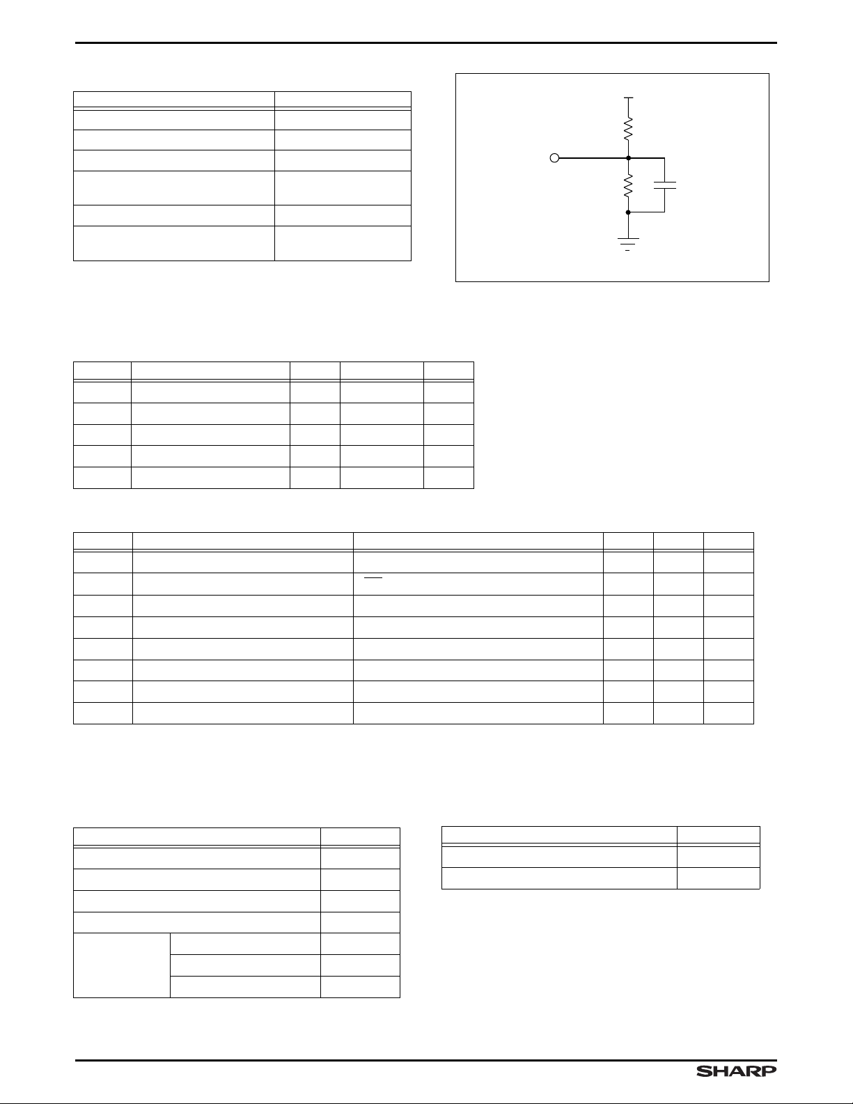
ABSOLUTE MAXIMUM RATINGS
1.1 k Ω
680 Ω
+5 V
30 pF
*
540235-3
PARAMETER RATING
Supply V olta ge to VSS Potential –0.5 V to 7 V
Signal Pin Voltage to VSS Potential –0.5 V to VCC + 0.5 V
DC Output Current
Temperature Range with Power
Applied
2
Storage T emperature Range
Power Dissipation (PLCC Pack-
age Limit)
NOTES:
1. Only one output may be shorte d at a time, for a period not
exceeding 30 seconds.
2. Measured with clocks idle.
1
75 mA
±
–55°C to 125°C
–65°C to 150°C
2 W
DEVICE
UNDER
TEST
*
INCLUDES JIG AND SCOPE CAPACITANCES
Figure 4. Output Lo ad Cir cu it
OPERATING RANGE
SYMBOL PARAMETER MIN. MAX. UNIT
T
A
V
CC
V
SS
V
IL
V
IH
T emperature, Ambient
Supply Voltage
Supply Voltage
Logic LOW Input Voltage
Logic HIGH Input Voltage
070C
4.5 5.5 V
00V
–0.5 0.8 V
2.0 V
+ 0.5 V
CC
DC ELECTRICAL CHARACTERISTICS (Over Operating Range)
SYMBOL PARAMETER TEST CONDITIONS MIN. MAX. UNIT
I
LI
I
LO
V
OH
V
OL
I
CC
I
CC2
I
CC3
I
CC4
NOTES:
1. Output load is disconnecte d.
2. I
CC
outputs open; and, for ICC and I
AC TEST CONDITIONS
Input Pulse Leve ls VSS to 3 V
Input Rise and Fal l T i mes (10% to 90 %) 3 ns
Input Timing Reference Levels 1.5 V
Output T i ming R efe renc e Level s 1.5 V
Output Load,
Timing Tests
(Figure 5)
Input Leakage VCC = 5.5 V , VIN = 0 V to V
I/O Leakage
OE ≥ VIH, 0 V ≤ V
OUT
≤ V
CC
CC
–10 10
–10 10
Output HIGH Voltage IOH = –8.0 mA 2.4 V
Output LOW Voltage IOL = 16.0 mA 0.4 V
Average O pe ra ting Supply Current
Average Sta nd by Su pply Current
Power-Down Supply Current
Power-Down Supply Current
, I
CC2
, and I
are dependent up on actual output loading, and ICC and I
CC3
CC4
, operating at mini mum cycle times.
1,2
Measured at fCC = 50 MHz 245 mA
2
All inputs = V
2
2
All inputs = VCC – 0.2 V (clocks idle) 1 mA
All inputs = VCC – 0.2 V (clocks at 50 MHz) 1 mA
(clocks idle) 25 mA
IHMIN
are also dependent on cycle rates. Specified values are with
CC4
CAPACITANCE
PARAMETER RATING
(Top Resistor)
R
1
(Bottom Resistor)
R
2
(Load Capacitance) 30 pF
C
L
1.1k
680
Ω
Ω
CIN (Input Capacitance) VIN = 0 V 9 pF
C
(Output Ca pa ci tance) V
OUT
PARAMETER RATING
= 0 V
OUT
9 pF
A
µ
A
µ
BOLD ITA LIC = Enhanced Operating Mode
8
Page 9

2048 x 18/4096 x 18 Synchronous FIFOs LH540235/45
AC ELECTRICAL CHARACTERISTICS
SYMBOL PARAMETER
f
CC
t
A
t
CLK
t
CLKH
t
CLKL
t
DS
t
DH
t
ENS
t
ENH
t
RS
t
RSS
t
RSR
t
RSF
t
OLZ
t
OE
t
OHZ
t
WFF
t
REF
t
PAF
Clock Cycle Frequency
Data Access T ime 2 12 3 15 3 20
Clock Cycle Time
Clock HIGH Time 8 10 14
Clock LOW Time
Data Setup Time 5 6 7
Data Hold Time 2 2 2
Enable Setup Time
Enable Hold Time 2 2 2
Reset Pulse Width
Reset Setup Time
Reset Recove ry T i m e
1
2
2
Reset to Flag and Output Time 30 35 40
Output Enab le t o O ut pu t in Low-Z
2
Output Enable t o Outpu t Valid
Output Enable t o Outpu t in Hi gh-Z
2
Write Clo ck to Full Flag
Read Clock to Em pty Flag 12 15 20
Clock to Progra mm able Almo st-F ull Flag (ID T-Compatible
Operating M ode)
–20 –25 -35
MIN. MAX. MIN. MAX. MIN. MAX.
50 40 28.6
20 25 35
81014
567
20 25 35
12 15 20
12 15 20
000
91215
19112115
12 15 20
14 17 23
t
PAE
t
HF
t
PAFS
t
PAES
t
HFS
t
XO
t
XI
t
XIS
t
SKEW1
t
SKEW2
NOTES:
1. Pulse widths less than the s t ate d mi nimum values may cause incorrect operation.
2. Values are guaranteed by design; not currently tested.
3. These times also apply to the Programmable-Almost-Full and Half-Full flags when they are synchronized to WCLK.
4. These times also apply to the Half-Full and Programmable-Almost-Empty flags when they are synchronized to RCLK.
Clock to Progr amm abl e Almo st -Emp ty Fla g (I DT-Compatibl e
Operating M ode)
Clock to Half-Full Flag (IDT-Compatible O p er ating Mode)
Clock to Progra mmab le Alm ost- Fu ll Fl ag (En hanc ed
Operating Mode)
Clock to Progra mmab le Alm ost- Emp ty Fl ag (En hanc ed
Operating Mode)
Clock to Half -F ull Flag (Enhanced Operating Mode)
14 17 23
14 17 23
14 17 23
14 17 23
14 17 23
Clock to Expa ns io n- O ut 12 15 20
Expansion-In Pu ls e Wi dt h
8913
Expansion-In Setup Time 8 9 14
Skew Tim e Betwee n Rea d Clock and Wr it e Clock for Fu ll Fl ag
Skew Tim e Betwee n W ri te Cloc k and Rea d Clo ck for Em pty F lag
3
91116
4
91116
BOLD ITALIC = Enhanced Operating Mode
Rev. B, 8/8/96
9
Page 10
LH540235/45 2048 x 18/4096 x 18 Synchronous FIFOs
DESCRIPTION OF SIGNALS AND OPERATING SEQUENCES
EMODE
1
H
1
H
H
H
Table 1. Grouping-Mode Determination
WXI/
WEN
RXI/
2
REN
FL/
2
RT
HHH
HHL
HLX
LHX
During a Reset Operation
MODE
Cascaded
2
Slave
Cascaded
Master
2
(Reserved)
(Reserved)
WXO/HF
USAGE
WXO WXI RXI FL RXO
WXO WXI RXI FL RXO
–––––
–––––
5
WXI/
USAGE
WEN
RXI/
2
REN
USAGE
2
FL/
RT
USAGE
RXO
/EF
USAGE
(Not
H
LL H
3
During
HF) (none) (none)
(
(RT)
(none)
Allowed
Reset)
3
H
LL L
Standalone HF (none) (none)
RT
(none)
(Not
LX X
H
3
During
HF) (WEN2)(REN2)(RT) (EF2)
(
Allowed
Reset)
Interlocked
LX X
NOTES:
1. In IDT-compatib l e c ascading, a reset operation fo rces
HIGH for the (n + 1)st FIFO.
2. The terms ‘master’ and ‘slave’ r efe r to IDT-compatible cascad ing. In pipelined cascading
3. Once grouping mode has been determined during a reset operation, FL/RT then may go HIGH to activate a retransmit operation.
EMODE must be asserted for access to the Control Register to be enabled. Also, FIFOs being used in a pipelined-cascading
4.
configuration should be in Interlocked Paralleled mode.
5. Setup-time and recovery-time specifications apply during a reset operation.
3
L
Paralleled
WXO/HF and RXO/
HF WEN
4
EF2
2
HIGH for the nth FIFO, thus for cing WXI/
4
, there is no such distinction.
REN
2
RT EF
WEN2
2
and RXI/
2
REN
2
I/O PIN
I WXI /
O
I RXI/
O
I FL/
NOTE:
1.
FL/RT may be grounded if
BOLD ITA LIC = Enhanced Operating Mode
WEN
2
WXO/HF To WXI ((n+1 )s t FI FO ) To WXI ( (n+1)st FIFO) Becomes HF
REN
2
RXO
/EF
2
RT
DEPTH-CASCADED
MASTER
From WXO (( n-1)st FIFO) From WXO (( n-1)st FIFO) Grounded
From RXO ((n-1)st FIFO) From RXO ((n-1)st FIFO) Grounded
To RXI ((n+1)st F IFO) T o R XI ((n+1)st FIFO) Unused
Grounded (Logic LOW) Logic HIGH
the Retransmit fa cility
Table 2. Expansion-Pin Usage According to
Grouping Mode
IDT-COMPATIBLE OPERATING MODE
DEPTH-CASCADED
SLAVE
is not being us ed .
STANDALONE
Becomes RT1Becomes RT
ENHANCED
OPERATING MODE
INTERLOCKED
PARALLELED
From FF (other FIFO)
Becomes HF
From EF (other FIFO)
Becomes EF
2
1
10
Page 11

2048 x 18/4096 x 18 Synchronous FIFOs LH540235/45
Table 3. Selection of Read and Write Operations
LD WEN
3,4
L X X – – No operation.
LL L
LL H
LH H
LH L X
LH H X
HL X
HX L X
HL X – X
HH X X X
H X L X – No read oper atio n.
HX H X X
HL L – –
H H H X X No operation.
KEY:
H = Logic ‘HIGH’; L = Logic ‘LOW’; X = ‘Don’t-care’ (logic ‘HIGH,’ logic ‘LOW,’ or any transition);
∧
= A ‘LOW’-to-‘HIGH’ tra ns ition; – = Any condition EXCEPT a ‘LOW’-to-‘HIGH’ transition.
NOTES:
1. The selection of a programmable register to be written or read is controlled by two simple state machines. One state machine controls the selection for writi n g; the other state machine cont ro l s the selection for reading. Th ese two state machines op erate independently of each other.
Both state machines are reset to point to Word 0 by a r es et o pe ra t ion .
both state machines are also reset to point to Word 0 by deassertion of LD after LD has been asserted (that is, by a rising edge of
LD), followed by a valid memory a r r ay w r ite cy cle for t h e w riting-control state machine and/or by a valid memory a rr ay r ead cy c le
for the reading-control state machine.
2. The order of the two programmable registers which are accessible in IDT-Compatible Operating Mode, as selected by either state machine, is
always:
Word 0: Almost-Empty Offset Register
Word 1: Almost-Ful l O ffse t Regi st er
Word 0: Almost-Empty Offset Register
...
(repeats indefini te l y)
...
The order of the three programmable registers which are accessible in Enhanced Operating Mode, as selected by either state
machine, is always:
Word 0: Almost-Empty Offset Register
Word 1: Almo st-Fu ll Of fse t Reg ister
Word 2: Control Register
Word 0: Almost-Empty Of fset Register
(repeats indefinitely)
Note that, in IDT-Compatible Operating Mode, W or d 2 is n ot a cc es se d; Word 0 and Word 1 alternate.
3. After normal FIFO operatio n h as begun, writing new contents into either of the offset regi sters should only be done w he n the FIFO is empty.
4. WEN2, REN2, and OE may be ANDed terms in the enabling of read and write operations, according to the state of the EMODE control
input and of Control Register bit 05.
……
……
REN
3,4
WCLK RCLK ACTION
∧∧
∧
∧
∧
Illegal combin atio n, wh ich wil l caus e erro rs.
Write to a programmable re gi st er.
X
X Hold present value of programmable-register write counter, and do not write.
Read from a programmable regi st er.
∧
Hold present value of programmable-register read counter, and do not read.
∧
Normal FIFO write operation.
X
Normal FIFO read operation.
∧
No write operation.
No write operation.
No read op er ation.
No operation.
In the Enhanced Operating Mode, if Control Register bit 00 is set,
1
2
1
2
BOLD ITALIC = Enhanced Operating Mode
11
Page 12
LH540235/45 2048 x 18/4096 x 18 Synchronous FIFOs
Table 4. Status Flags
NUMBER OF UNREAD DATA WORDS PRESENT WITHIN FIFO
2048 × 18 FIFO 4096 × 18 FIFO
1, 2
FULL
FLAG
FF PAF HF PAE EF
MIDDLE FLAGS
EMPTY
FLAG
0 0 HHHLL
1 to q 1 to q H H H L H
(q + 1) to 1024 (q + 1) to 2048 HHHHH
1025 to (2048 – (p + 1)) 2049 to (4096 – (p + 1)) H H L H H
(2048 – p) to 2047 (4096 – p) to 4095 H L L H H
2048 4096 L L L H H
NOTES:
1. q = Programmable-Almos t-Em p ty Offset value. (Default va l ue : q = 1 27.)
2. p = Programmable-Almos t-F u l l O ffset value. (Default value: p = 127.)
3. Only 11 (2048 × 18), or all 12 (409 6 × 18), of the 12 of fse t-value-register bits shou l d b e p rogrammed. The unneeded m o st-significant-end
2048 × 18 bit should be LOW (zero).
4. The flag output is delayed b y o ne full clock cycle in Enh an ce d O perating Mode, when synchronous operation is speci fi e d for intermediate flags.
BOLD ITA LIC = Enhanced Operating Mode
12
Page 13
2048 x 18/4096 x 18 Synchronous FIFOs LH540235/45
DESCRIPTION OF SIGNALS AND OPERATING SEQUENCES (cont’d)
Table 5. Control-Reg ister Format
COMMAND
REGISTER
BITS
CODE
VALUE AFTER RESET FLAG
EMODE = H EMODE = L
AFFECTED,
IF ANY
DESCRIPTION NOTES
Deasserti on of LD does not
L
reset the progra mmab leregister writ e po inter and
IDT - co mpatible addressing
of programmable registers.
read pointer.
Deasserti on of
LD resets
the programmable-register
write pointer and read
00
H
LH–
pointer to address Word 0,
the Programm ab le -Al mo stEmpty-Flag-O f fse t Regis ter.
The change takes effect
Non-ambiguous
addressing of
programmable r e gi sters.
after a valid writ e opera tion
or a valid read operation,
respectively, to the mem ory
array.
↑
01
03, 02
04
L
H
LL
LH
HL,
HH
L
H
LH
PAE
LL HH HF
L
H
PAF
Set by
↑
Set and reset b y
Set by
↑
Set and reset b y
Set and reset b y
Set by
↑
Set and reset b y
RCLK, reset by
WCLK.
↑
WCLK, reset by
RCLK.
↑
WCLK, reset by
RCLK.
↑
RCLK.
↑
RCLK.
↑
WCLK.
↑
WCLK.
OE has no e ffect on an
L
internal read operation,
apart from disablin g the
outputs.
05
LH–
H
Deasserti on of OE inhibits
a read ope ration; whenever
the data outputs Q
– Q
0
17
are in the h igh-Z state, the
read pointer does n ot
advance.
L
06
11, 10,
09, 08, 07
NOTES:
When
1.
IDT72235B/45B FIFO of similar depth and speed grade. Under these conditions, the
ternal system which inclu des th e FIFO .
If
2.
EMODE
LOW) during a reset operation, Control Register bits 00-05 are forced HIGH, and remain HIGH until changed. Control Register bits
06-11 are unaffected by EMODE.
H
LLLLL LLLLL LLLLL
is HIGH, and
EMODE
is not asserted (is HIGH),
LL
Control Register bits 00-05 are LOW,
Control Register bits 00-05 remain LOW
–
–
Reserved.
Reserved. Reserved.
the FIFO behaves in a manner functionally equivalent to the
Control Register
after a reset operation.
Asynchronous flag
clocking.
Synchronous flag clocking.
Asynchronous flag
clocking.
Synchronous flag clocking
at output port.
Synchronous flag clocking
at input port.
Asynchronous flag
clocking.
Synchronous flag clocking.
Allows the read-address
pointer to ad va nce even
when Q
– Q17 are not
0
driving the output bus.
Inhibits the re ad -a dd res s
pointer from a dv anci ng
when Q
– Q17 are not
0
driving the output bus;
thus, guards agai nst da ta
loss.
Future use to c on tro l de pt h
cascading and in ter lock ed
paralleling.
is not visible or accessible to the ex-
However, if EMODE is asserted (is
BOLD ITALIC = Enhanced Operating Mode
13
Page 14

LH540235/45 2048 x 18/4096 x 18 Synchronous FIFOs
Data Inputs
DATA IN (D0 – D17)
Data, programmable-flag-offset values, and
Register
D
0
trol-Register
codes are input to the FIFO as 18-bit words on
– D17. Unused bit positions in offset-value
words should be zero-filled.
Control-
and Con-
Control Inputs
RESET (RS)
The FIFO is reset whenever the asynchronous Reset
RS) input is taken to a LOW state. A reset operation is
(
required after power-up, before the first write operation
may occur. The state of the FIFO is fully defined after a
reset operation. If the default values which are entered
into the Programmable-Flag-Offset-Value Registers
the Control Register
able, then no device programming is required. A reset
operation initializes the FIFO’s internal read-address and
write-address pointers to the FIFO’s first physical memory
location. The five status flags,
are updated to indicate that the FIFO is completely empty;
thus, the first three of these are reset to HIGH, and the
last two are reset to LOW . The flag-of fset values for
PAE each are initialized to 12710. If
and
being asserted (i.e., if
Register
to operate in the IDT72235B/45B-Compatible Operating
Mode. Until a write operation occurs, the data outputs
D
0
bits are initialized to LOW, to configure the FIFO
– D17 all are LOW whenever OE is LOW.
by a reset operation are accept-
FF, PAF, HF, P AE, and EF,
EMODE
EMODE
is HIGH), all
ENHANCED OPERATING MODE (EMODE)
Whenever
EMODE is asserted during a reset operation, Control Register bits 00-05 remain HIGH
rather than LOW after the completion of the reset
operation. Thus,
EMODE has the effect of activating
all of the Enhanced-Operating-Mode features during
a reset operation. Subsequently, they may be individually disabled or re-enabled by changing the setting of Control-Register bits. The behavior of these
Enhanced-Operating-Mode features is described in
Table 5. For permanent Enhanced-Operating-Mode
operation,
trol of
EMODE must be grounded; dynamic con-
EMODE during system operation is not recom-
mended.
Asserting
causes
EMODE during a reset operation also
WXI/WEN2 to be configured as WEN2, and
RXI/REN2 to be configured as REN2, to support in terlocked-paralleled operation of two FIFOs ‘side by
side’ (see Figu re 28). Additionally ,
ured as
EF2, which duplicates the EF signal with one
RXO/EF2 is config-
extra RCK cycle delay, in order to provide proper
timing for ‘pipelined’ cascaded op eration.
and
PAF
is not
Control
WRITE CLOCK (WCLK)
A rising edge (LOW-to-HIGH transition) of WCLK initiates a FIFO write cycle if
ble-register write cycle if
and all input-side synchronous control inputs, must meet
setup and hold times with respect to the rising edge of
WCLK. The input-side status flags are meaningful after
specified time intervals, following a rising edge of WCLK.
Conceptually , the WCLK input receives a free-running,
periodic ‘clock’ waveform, which is used to control other
signals which are edge-sensitive. However, there actually
is not any absolute requirement that the WCLK waveform
must
be periodic. An ‘asynchronous’ mode of operation
is in fact possible, if
is, is continuously held LOW), and WCLK receiv es aperiodic ‘clock’ pulses of suitable duration. There likewise is
no requirement that WCLK must have any particular
synchronization relation to the read cloc k RCLK. These
two clock inputs may in fact receive the same ‘clock’
signal; or they may receive totally-different signals, which
are not synchronized to each other in any way.
WRITE ENABLE (
Whenever
HIGH, and the FIFO is not full, an 18-bit data word is
loaded into the effective input register for the memory
array at every WCLK risi ng edge (LOW-to-HIGH transition). Data words are stored into the two-port memory
array sequentially, regardless of any ongoing read operation. Whenever
input register retains whatever data word it contained
previously, and no new data word gets loaded into the
memory array.
To prevent overrunning the internal FIFO boundaries,
further write operations are inhibited whenever the Full
FF) is being asserted (is LOW). If a valid read
Flag (
operation then occurs, upon the completion of that read
FF again goes HIGH after a time t
cycle
write operation is allowed to begin whenever WCLK
makes another LOW-to-HIGH transition. Effectively,
WEN is overridden by FF; thus, during normal FIFO
operation,
WEN is being asserted (is LOW) and LD is
WEN is not being asserted (is HIGH), the
WEN has no effect when the FIFO is full.
LD is HIGH, or a programma-
LD is LOW. The 18 data inputs,
WEN is continuously asserted (that
WEN)
, and another
WFF
In the Enhanced Operating Mode, WXI/WEN2 functions as WEN
, an additional duplicate (albeit asser-
2
tive-HIGH) write-enable input, in order to provide
an‘interlocking’ mechanism for reliable synchronization of two parallel ed FIFOs. To control w riting,
is ANDed with WEN; this logic-AND function
WEN
2
WEN •• WEN2) then behaves like WEN in the forego-
(
ing description.
BOLD ITA LIC = Enhanced Operating Mode
14
Page 15

2048 x 18/4096 x 18 Synchronous FIFOs LH540235/45
DESCRIPTION OF SIGNALS AND
OPERA TING SEQUENCES (cont’d)
READ CLOCK (RCLK)
A rising edge (LOW-to-HIGH transition) of RCLK initiates a FIFO read cycle if
ble-register read cycle if
synchronous control inputs must meet setup and hold
times with respect to the rising edge of RCLK. The 18 data
outputs, and the output-side status flags, are meaningful
after specified time intervals, following a rising edge of
RCLK.
Conceptually , the RCLK input receives a free-running,
periodic ‘clock’ waveform, which is used to control other
signals which are edge-sensitive. However, there actually
is not any absolute requirement that the RCLK waveform
must
be periodic. An ‘asynchronous’ mode of operation
is in fact possible, if
is, is continuously held LOW), and RCLK receives aperiodic ‘clock’ pulses of suitable duration. There likewise is
no requirement that RCLK must have any particular
synchronization relation to the write clock WCLK. These
two clock inputs may in fact receive the same ‘clock’
signal; or they may receive totally-different signals, which
are not synchronized to each other in any way.
READ ENABLE (
Whenever
REN)
REN is being asserted (is LOW), and the
FIFO is not empty , an 18-bit data word is loaded into the
output register from the memory array at every RCLK
rising edge (LOW-to-HIGH transition). Data words are
read from the two-port memory array sequentially , regardless of any ongoing write operation. Whenever
not being asserted (is HIGH), the output register retains
whatever data word it contained previously, and no new
data word gets loaded into it from the memory array.
T o prevent underrunning the internal FIFO boundaries,
further read operations are inhibited whenever the Empty
EF) is being asserted (is LOW). If a valid write
Flag (
operation then occurs, upon the completion of that write
EF again goes HIGH after a time t
cycle
read operation is allowed to begin whenever RCLK
makes another LOW-to-HIGH transition. Effectively ,
is overridden by
EF; thus, during normal FIFO operation,
REN has no effect when the FIFO is empty.
In the Enhanced Operating Mode, one (or, sometimes two) additional read-enable inputs may be
ANDed with
REN to control reading, depending on
the state of Control-Register bit 05. The additional
read-enable input(s) are REN
LD is HIGH, or a programma-
LD is LOW. All output-side
REN is continuously asserted (that
REN is
, and another
REF
REN
(and OE).
2
Also in the Enhanced Operating Mode,
RXI/REN
functions as REN2, an additional duplicate (albeit
assertive-HIGH) Read-Enable input, in order to provide an ‘interlocking’ mechanism for reliable
synchronization of two p ar alleled F IFOs.
Also, if Control Register bit 05 is HIGH,
OE takes
on the extra role of serving as yet another duplicate
read-enable input, in addition to its usual function of
controlling the FIFO’s data outputs, in order t o inhibit
further read operations whenever the FIFO’s data
outputs are disabled, and thereby to prevent data
loss under some circumstances.
OUTPUT ENABLE (OE)
OE is an assertive-LOW, asynchronous, output
enable. In the IDT-Compatible Operating Mode,
OE has
only the effect of enabling or disabling the data outputs
– Q17. That is, disabling Q0 – Q17 does not inhibit a
Q
0
read operation, for data being transmitted to the output
register; the same data will remain available later, when
the outputs are again enabled, unless subsequently overwritten. When Q
– Q17 are enabled, each of these 18
0
data outputs is in a normal HIGH or LOW state, according
to the bit pattern of the data word in the output register.
When Q
– Q17 are disabled, each of these outputs is in
0
the high-Z (high-impedance) state.
In the Enhanced Operating Mode, if Control Reg-
ister bit 05 is HIGH,
OE behaves as an additional
read-enable control input, as well as enabling and
disabling the data outputs Q
– Q17. Under these
0
circumstances, incrementing the read-address
pointer is inhibited whenever Q
– Q17 are in the
0
high-Z state. Thus, ‘reading’ successive words which
fail ever to reach the outputs is prevented, as a
safeguard against data loss.
LOAD (LD)
three
The Sharp LH540235/45 FIFOs contain
18-bit
programmable registers. The contents of these three
registers may be loaded with data from the data inputs
– D17, or read out onto the data outputs Q0 – Q17. The
D
0
first two registers are the Programmable-Flag-OffsetValue Registers, for the Programmable Almost-Empty
P AE) and the Programmable Almost-Full Flag (PAF)
Flag (
respectively.
The third register is the Control Register ,
which includes several configuration-control bits
for selectively enabling and disabling Sharp’s
Enhanced-Operating-Mode features.
2
BOLD ITALIC = Enhanced Operating Mode
15
Page 16

LH540235/45 2048 x 18/4096 x 18 Synchronous FIFOs
WORD 0
WORD 1
WORD 2
12 7
CONTROL-REGISTER BITS:
6
Future use to control depth cascading and interlocked paralleling.
5
Enables suppressing reading whenever data outputs are disabled.
4
Makes PAF synchronous.
3
2
Makes HF synchronous. (See the Control-Register Format
table for the encoding of bits 02-03.)
Makes PAE synchronous.
1
Selects reinitialized addressing of the programmable registers.
0
NOTES:
1. Default offset values all are 127
2. Bits 11-17 (LH540235) or bits 12-17 (LH540245) of both offset-value registers should
in all cases be programmed LOW (zero).
3. This bit position is used for offset values in the LH540245 only. In the LH540235, it
always should be programmed LOW.
4. See the Control-Register Format table for the default states of the Control Register,
for EMODE = HIGH (IDT-Compatible Operating Mode) and for EMODE = LOW (Enhanced Operating Mode).
The Control Register is not accessible or visible in IDT-Compatible Operating Mode.
5. The assertion of EMODE (LOW) forces Control Register bits 00-05 HIGH during a reset operation.
After that, these bits may be programmed at will.
= Reserved. Do not load with non-zero information.
BOLD ITALIC = Enhanced Operating Mode.
= 7F16.
10
3
10
3
1112 10
Reserved for
future use.
PROGRAMMABLE-ALMOST-EMPTY-FLAG-OFFSET VALUE
PROGRAMMABLE-ALMOST-FULL-FLAG-OFFSET VALUE
CONTROL REGISTER
6
See Table 5 for a
more complete
description of these
effects.
4, 5
4
5
3
1, 2
0111217
1, 2
017
2
1 0
12345617
540235-4
011
Figure 5. Programmable Registers
None of these three registers makes use of all of its
available 18 bits. Figure 6 shows which bit positions of
each register are operational. The two ProgrammableFlag-Offset-V alue Registers each contain an offset value
in bits 0-10 (LH540235) or bits 0-11 (LH540245); bits
1 1-17 (LH540235) or bits 12-17 (LH540245) are unused.
The default values for both offsets are 127
The
Control Register
ure 6 and in Table 5. For the
configuration is shown in Fig-
Control Register
IDT-Compatible Operating Mode, with
.
10
EMODE
, in the
deasserted (HIGH), the default value for all Control-Regist er
bits is zero (LO W).
EMODE asserted (LOW), the default value for
with
In the Enhanced Operating Mode,
bits 00-05 is HIGH, and the default value for bits 06-1 1
is LOW.
BOLD ITA LIC = Enhanced Operating Mode
16
Whenever
LD and WEN are simultaneously being
asserted (are both LOW), the 18-bit data word from the
data inputs D
– D17 is written into the Programmable-
0
Almost-Empty-Flag-Offset-Value Register at the first rising edge (LOW-to-HIGH transition) of the write clock
(WCLK). (See Table 3.) If
LD and WEN continue to be
simultaneously asserted, another 18-bit data word from
the data inputs D
– D17 is written into the Programma-
0
ble-Almost-Full-Flag-Offset-Value Register at the second
rising edge of WCLK.
Page 17

2048 x 18/4096 x 18 Synchronous FIFOs LH540235/45
DESCRIPTION OF SIGNALS AND
OPERA TING SEQUENCES (cont’d)
What happens next is determined by the state of the
EMODE
18-bit word from the data inputs D
into the Programmable-Almost-Empty-Flag-Offset-Value
Register again.
18-bit data word from the data inputs D
written into the Control Register at the third rising
edge of WCLK . At the fourth rising edge of WCLK,
writing again occurs to the Programmable-AlmostEmpty-Flag-Offset-Value Register; and the same
three-step writing sequence gets repeated on subsequent WCLK rising edges.
use of by the 2048-word LH540235, and the lower 12 bits
by the 4096-word LH540245.
for the Control Register, by both the LH540235 and
the LH540245
may occur in these offset-value
fields. However,
LOW, in order to maintain forward compatibility.
registers does not have to occur all at one time, or to be
effected by one single sequence of steps. Whenever
is being asserted (is LOW) but
(is HIGH), the FIFO’s internal programmable-registerwrite-address pointer maintains its present value, without
any writing actually taking place at each rising edge of
WCLK (see Table 3). Thus, for instance, one or two
programmable registers may be written, after which the
FIFO may be returned to normal FIFO-array-read/write
operation by deasserting
being asserted (are both LOW) the 18-bit data word
(zero-filled as necessary) from the Programmable-Almost-Empty-Flag-Offset-Value Register is read to the
data outputs Q
HIGH transition) of the read clock (RCLK) (see Table 3).
If
another 18-bit data word from the Programmable-AlmostFull-Flag-Offset-V alue Register is read to the data outputs
Q
EMODE
18-bit word again comes from the Programmable-AlmostEmpty-Flag-Offset-Value Register; it is read to the data
outputs Q
18-bit data word instead comes from the Control
Register; it is read to the data outputs Q
third rising edge of RCLK. At the fourth rising edge
of RCLK, reading again occurs from the Programmable-Almost-Empty-Flag-Offset-Value Register; and
control input. If it is deasserted (HIGH), the next
– D17 is written back
0
But, if EMODE is asserted (LOW), then still another
– D17 is
0
The lower 1 1 bits of these offset-value words are made
Six active bits are used
.
There is no restriction on the values which
and Control-Register
reserved
Writing contents to these two
bit positions must be encoded
or three
programmable
LD
WEN is not being asserted
LD (to HIGH).
Likewise, whenever
– Q17 at the first rising edge (LOW-to-
0
LD and REN are simultaneously
LD and REN continue to be simultaneously asserted,
– Q17 at the second rising edge of RCLK.
0
What happens next is determined by the state of the
control input. If it is deasserted (HIGH), the next
– Q17.
0
But, if EMODE is asserted (LOW), then the next
– Q17 at the
0
the same three-step reading sequence gets repeated
on subsequent RCLK rising edges.
Reading contents from these two
or three
programmable registers does not have to occur all at one time, or
to be effected by one single sequence of steps. Whenever
LD is being asserted (is LOW) but REN is not being
asserted (is HIGH), the FIFO’s internal programmableregister-read-address pointer maintains its present value,
without any reading actually taking place at each rising
edge of RCLK. (See Table 3.) Thus, for instance, one or
two programmable registers may be read, after which the
FIFO may be returned to normal FIFO-array-read/write
operation by deasserting
LD (to HIGH).
T o ensure correct operation, the simultaneous reading
and writing of a register should be avoided.
FIRST LOAD/
FL
/RT is a dual-purpose signal.
RETRANSMIT (FL/RT)
It is one of four input
signals which select the grouping mode in which the FIFO
operates after being reset; the other three of these input
WXI
WEN
signals are
four
are
/
possible grouping modes: standalone,
locked paralleled
RXI
,
/
REN2, and EMODE. Th er e
2
inter-
, cascaded ‘master’ or ‘first-load,’ and
cascaded ‘slave.’ The designations ‘master’ and ‘slave’
pertain to IDT-compatible depth cascading. Tables 1 and
2 show the signal encodings which select each grouping
mode.
In standalone or paralleled operation, the
FL/RT pin
should be grounded for strict IDT72235B/45B-compatible
operation.
the state of the
However, if it is taken HIGH, regardless of
EMODE control input, the FIFO’s
internal read-address pointer is reset to address the
FIFO’s first physical memory location, without the
other usual reset actions being taken; in particular,
the FIFO’s internal write-address pointer is unaffected. Subsequent read operations may then again
read out the same block of data, delimited by the
FIFO’s first physical memory location and the current
value of the write pointer, as was read o ut previously.
There is no limit on the number of times t hat a blo ck
of data may be retransmitted. The only restrictions
are that neither the read-address pointer nor the
write-address pointer may ‘wrap around’ and add ress
the FIFO’s first physical memory location a second
time during the retransmission process,
and that
the
retransmit facility is unavailable during cascaded operation.
In IDT-compatible cascaded operation,
FL/RT is
grounded for the ‘master’ or ‘first-load’ FIFO, to distinguish
it from the other ‘slave’ FIFOs in the cascade, which must
all have their
FL/RT inputs HIGH during a reset operation
(see again Tables 1 and 2). The cascade will not operate
correctly either without any ‘master ’ FIFO, or with more
than one ‘master’ FIFO.
BOLD ITALIC = Enhanced Operating Mode
17
Page 18

LH540235/45 2048 x 18/4096 x 18 Synchronous FIFOs
WRITE EXPANSION INPUT/
(WXI/
WXI
WEN
/WEN
)
2
is a dual-purpose signal. It is one of four
2
WRITE ENABLE 2
input signals which select the grouping mode in which the
FIFO operates after being reset; the other three of these
input signals are
possible grouping modes: standalone,
four
are
locked paralleled
FL/RT, RXI/
REN2, and EMODE
, cascaded ‘master ’ or ‘first-load,’ and
. There
inter-
cascaded ‘slave.’ The designations ‘master’ and ‘slave’
pertain to IDT-compatible depth cascading. Tables 1 and
2 show the signal encodings which select each grouping
mode.
In standalone operation,
WXI/
WEN
and RXI/
2
REN
both must be grounded so that the FIFO comes up in the
standalone grouping mode after a reset operation.
interlocked-paralleled operation,
WXI/WEN2 is tied to
In
FF of the other paralleled FIFO, and RXI/REN2 is tied
EF of that same other FIFO. This interconnection
to
scheme ensures that both FIFOs will operate
together , and remain coordinat ed, regard less of timing skews.
In cascaded operation, WXI/
WEN
is connected to the
2
WXO (Write Expansion Output; actually WXO/HF) output
RXI/
REN
WXI/
is likewise
2
WEN
and
2
of the previous FIFO in the cascade.
connected to the
RXO/
EF
) output of that previous FIFO. A reset operation
2
forces
WXO/HF and RXO/
RXO (Read Expansion Output; actually
EF
HIGH for each FIFO;
2
consequently, all FIFOs with their
RXI/
REN
inputs thus connected come up i n one of the
2
two cascaded grouping modes, according to whether
FL/RT inputs are grounded or tied HIGH (see T ables
their
1 and 2).
READ EXPANSION INPUT/
(RXI/
RXI
REN
/REN2
)
2
is a dual-purpose signal. It is one of four
READ ENABLE 2
input signals which select the grouping mode in which the
FIFO operates after being reset; the other three of these
input signals are
four
are
FL/RT, WXI/
possible grouping modes: standalone,
locked-paralleled
, cascaded ‘master’ or ‘first-load,’ and
WEN2, and EMODE
. There
inter-
cascaded ‘slave.’ The designations ‘master’ and ‘slave’
pertain to IDT-compatible depth cascading. Tables 1 and
2 show the signal encodings which select each grouping
mode.
In standalone operation,
and RXI/
2
REN
WXI/
WEN
both must be grounded, so that the FIFO comes up in the
standalone grouping mode after a reset operation.
interlocked-paralleled operation,
WXI/WEN2 is tied to
In
FF of the other paralleled FIFO, and RXI/REN2 is tied
EF of that same other FIFO. This interconnection
to
scheme ensures that both FIFOs will operate together , and remain coord inated, regardless o f timing
skews.
In cascaded operation, RXI/
REN
is connected to
2
RXO (Read Expansion Output; actually RXO/
WXI/
previous FIFO in the cascade.
connected to
WXO (Write Expansion Output; actually
WEN
WXO/HF) output of that previous FIFO. A reset operation
RXO/
EF
forces
consequently, all FIFOs with their
WXI/
WEN
and WXO/HF HIGH for each FIFO;
2
RXI/
inputs thus connected come up in one of the
2
two IDT-compatible cascaded grouping modes, according to whether their
FL/RT inputs are grounded or tied
HIGH (see again Tables 1 and 2).
Data Outputs
2
DATA OUT (Q0 – Q17)
Data, programmable-flag-offset values, and
Register
on Q
and
codes are output from the FIFO as 18-bit words
– Q17. Unused bit positions in offset-value words
0
Control-Register
words are zero-filled.
Control/Status Outputs
FULL FLAG (FF)
FF goes LOW whenever the FIFO is completely full.
That is, whenever the FIFO’s internal write pointer has
completely caught up with its internal read pointer; so that,
if another word were to be written, it would have to
overwrite the unread word which is now in position for
reading out by the next requested read operation. Under
these conditions, the FIFO is filled to its nominal capacity,
which is 2048 18-bit words for the LH540235 or 4096
18-bit words for the LH540245 respectively. Write operations are inhibited whenever
assertion or deassertion of Write Enable (
If the FIFO has been reset by asserting
initially is HIGH. But, whenever no read operations have
been performed since the completion of the reset opera-
FF goes LOW after 2048 write operations for the
tion,
LH540235, or after 4096 write operations for the
LH540245 (see Table 4).
FF gets updated after a LOW-to-HIGH transition of the
Write Clock (WCLK).
PROGRAMMABLE ALMOST-FULL FLAG (
P AF goes LOW whenever the FIFO is ‘almost’ full; that
is, whenever subtracting the value of the FIFO’s internal
2
read pointer from the value of its internal wr ite pointer
yields a difference which is less than the value of the
Programmable-Almost-Full-Flag Offset ‘p.’ The subtraction is performed using modular arithmetic, modulo the
total nominal number of 18-bit words in the FIFO’s physical memory , which is 2048 for the LH540235 or 4096 for
the LH540245 respectively.
FF is LOW , regardless of the
EF
)) of the
2
is likewise
2
REN
and
2
Control-
WEN).
RS (LOW), FF
PAF)
BOLD ITA LIC = Enhanced Operating Mode
18
Page 19

2048 x 18/4096 x 18 Synchronous FIFOs LH540235/45
DESCRIPTION OF SIGNALS AND
OPERA TING SEQUENCES (cont’d)
The default value of ‘p’ after the completion of a reset
operation is 127
which does not exceed this total nominal number of words
for the device, as explained in the description of Load
LD).
(
If the FIFO has been reset by asserting
no read operations have been performed since the
completion of the reset operation,
(2048-p) write operations for the LH540235, or after
(4096-p) write operations for the LH540245 (see T able 4).
If p is still at its default value,
the FIFO is from seven-eighths full to completely full.
In the IDT-Compatible Operating Mode,
from HIGH to LOW only after a LOW-to-HIGH transition
of the Write Clock WCLK, and from LOW to HIGH only
after a LOW-to-HIGH transition of the Read Clock RCLK.
Thus, in this operating mode,
chronous flag.’
In the Enhanced Operating Mode, on the other
hand, PAF gets updated only after a LOW-to-HIGH
transition of the Write Clock WCLK, and thus behaves
as a ‘synchronous flag,’ whenever Control Register
bit 04 is HIGH (see Table 5).
WRITE EXPANSION OUT/HALF-FULL FLAG
(WXO/HF)
WXO/HF is a dual-purpose signal. In ‘standalone’
operation, it behaves as a Half-Full Flag (
ance with Table 4. In IDT-compatible ‘cascaded’ operation, it behaves as a Write Expansion Output (
signal to coordinate writing operations with the next FIFO
in the cascade. Under these same conditions, also, the
dual-purpose
as Write Expansion Input (
RXI) signals respectively.
Input (
When two or more LH540235 or LH540245 FIFOs are
‘cascaded’ to operate as a deeper ‘effective FIFO,’ in an
IDT-style ‘daisy-chain’ ring configuration, the Write Expansion Input (
of the previous FIFO in the ring, with
or ‘master’ FIFO being connected to
so as to complete the ring. Similar connections are made
for each FIFO in the ring, parallel to these
connections, for Read Expansion Input (
Expansion Output (
RXO).
When the last physical location has been written in a
FIFO operating in cascaded mode, a LOW-going pulse is
emitted by that FIFO on its
deactivated for writing at the nex t valid WCLK; and the
next FIFO in the ring is simultaneously activated for
. However, ‘p’ may be set to any value
10
RS (LOW), and
PAF goes LOW after
PAF is LOW whenever
P AF changes
P AF behaves as an ‘asyn-
HF), in accord-
WXO)
WXI/
WEN
and RXI/
2
REN
inputs behave
2
WXI) and Read Expansion
WXI) of each FIFO is connected to WXO
WXI of the ‘first-load’
WXO of the last FIFO
WXO-to-WXI
RXI) and Read
RXO/
EF
, when it is behaving as
2
WXO output, and the FIFO is
writing. Otherwise,
WXO remains constantly HIGH when-
ever the FIFO is operating in cascaded mode. This LOW-
WXO pulse serves as a ‘write token’ in the
going
‘token-passing’ FIFO-cascading scheme; it is passed on
to the next FIFO in the ring via its
WXI input. When this
next FIFO receives the write token, it is activated for
writing at the next valid WCLK.
The foregoing description applies both to the ‘first-load’
or ‘master’ FIFO in the ring, and to any and all ‘slave’
FIFOs in the ring. However,
WXO has no necessary
function for FIFOs operating in the ‘standalone’ mode.
Consequently , in that mode, the same output pin is used
HF; it follows that HF is not available as an output from
for
any FIFO which is operating in the IDT-compatible cascaded mode. A FIFO is initialized into ‘cascaded master’
mode, into ‘cascaded slave’ mode,
alleled mode
state of its
, or into standalone mode according to the
WXI/
WEN
, RXI/
2
inputs during a reset operation,
into interlocked-par-
REN
, and FL/RT control
2
and of EMODE
(see
Table 1, T able 2, and Table 5).
In standalone
or interlocked-paralleled
operation,
HF goes LOW whenever the FIFO is more than half full;
that is, whenever subtracting the value of the FIFO’s
internal read pointer from the value of its internal write
pointer yields a difference which is less than half of the
total nominal number of 18-bit words in the FIFO’s physical memory , which is 1024 for the LH540235 or 2048 for
the LH540245 respectively (see T able 4). The subtraction
is performed using modular arithmetic, modulo this total
nominal number of words, which is 2048 for the
LH540235 or 4096 for the LH540245 respectively.
If the FIFO has been reset by asserting
it is operating in standalone mode
mode, and no read operations have been per-
alleled
or in interlocked-par-
formed since the completion of the reset operation,
RS (LOW), and
HF
goes LOW after 1025 write operations for the LH540235,
or after 2049 write operations for the LH540245 (see
again Table 4).
In the IDT-Compatible Operating Mode,
HF changes
from HIGH to LOW only after a LOW-to-HIGH transition
of the Write Clock WCLK, and from LOW to HIGH only
after a LOW-to-HIGH transition of the Read Clock RCLK.
Thus, in this operating mode,
HF behaves as an ‘asyn-
chronous flag.’
In the Enhanced Operating Mode, on the other
hand, HF gets updated only after a LOW-to-HIGH
transition of the Read Clock RCLK, or else after a
LOW-to-HIGH transition of the Write Clock WCLK,
according to the setting of bits 03 and 02 of the
Control Register (see Tab le 5). Thus, in this mode HF
behaves as a ‘synchronous flag,’ and may be synchronized either to the input side of the FIFO (i.e., to
WCLK), or to the output side of the FIFO (i.e., to
RCLK).
BOLD ITALIC = Enhanced Operating Mode
19
Page 20

LH540235/45 2048 x 18/4096 x 18 Synchronous FIFOs
PROGRAMMABLE ALMOST-EMPTY FLAG (PAE)
P AE goes LOW whenever the FIFO is ‘almost empty’;
that is, whenever subtracting the value of the FIFO’s
internal write pointer from the value of i ts internal read
pointer yields a difference which is less than q + 1, where
‘q’ is the value of the Programmable-Almost-Empty-Flag
Offset. The subtraction is performed using modular arithmetic, modulo the total nominal number of 18-bit words
in the FIFO’s physical memory, which is 2048 for the
LH540235 or 4096 for the LH540245 respectively.
The default value of q after the completion of a reset
operation is 127
. However, q may be set to any value
10
which does not exceed this total nominal number of words
for the device, as explained in the description of Load
LD).
(
If the FIFO has been reset by asserting
RS (LOW), and
no write operations have been performed since the completion of the reset operation, then
P AE is LOW (see T able
4).
If q is still at its default value,
PAE is LOW whenever
the FIFO is from one-eighth full to completely empty.
In the IDT -Compatible Operating Mode,
P AE changes
from HIGH to LOW only after a LOW-to-HIGH transition
of the Read Clock RCLK, and from LOW to HIGH only
after a LOW-to-HIGH transition of the Write Clock WCLK.
Thus, in this operating mode,
P AE behaves as an ‘asyn-
chronous flag.’
In the Enhanced Operating Mode, on the other
hand,
PAE gets updated only after a LOW-to-HIGH
transition of the Read Clock RCLK, and thus behaves
as a ‘synchronous flag,’ whenever Control Register
bit 01 is HIGH (see Table 5).
EMPTY FLAG (EF)
EF goes LOW whenever the FIFO is completely empty .
That is, whenever the FIFO’s internal read poi nter has
completely caught up with its internal write pointer; so
that, if another word were to be read out, it would have to
come from the physical memory location which is now in
position to be written into by the next requested write
operation. Read operations are inhibited whenever
EF is
LOW, regardless of the assertion or deassertion of Read
Enable (
REN).
If the FIFO has been reset by asserting
RS (LOW), and
no write operations have been performed since the
completion of the reset operation, then
EF is LOW. (See
Table 4.)
EF gets updated after a LOW-to-HIGH transition of the
Read Clock RCLK.
READ EXPANSION OUT/
RXO/
EF
is a dual-purpose signal. In ‘standalone’
2
EMPTY FLAG 2
(RXO/
EF
2
operation, it has no function. In IDT-compatible ‘cascaded’ operation, it behaves as a Read Expansion Output
BOLD ITA LIC = Enhanced Operating Mode
RXO) signal to coordinate writing operations with the
(
next FIFO in the cascade. Under these same conditions,
RXI/
REN
also, the dual purpose
behave as Read Expansion Input (
sion Input (
WXI) signals respectively.
and WXI/
2
RXI) and Write Expan-
When two or more LH540235 or LH540245 FIFOs are
operating in IDT-compatible ‘cascaded’ mode as a deeper
‘effective FIFO,’ the dual-purpose
WXI/
WEN2
inputs behave as Read Expansion Input (RXI)
and Write Expansion Input (
WXI) signals respectively. An
RXI/
IDT-style cascade of these FIFO devices has a ‘daisychain’ ring configuration; the Read Expansion Input (
of each FIFO is connected to
RXO) of the previous FIFO in the ring, with RXI of the
as
RXO (RXO/
‘first-load’ or ‘master’ FIFO being connected to
the last FIFO so as to complete the ring. Similar connections are made for each FIFO in the ring, parallel to these
RXO-to-RXI connections, for Write Expansion Input
WXI) and Write Expansion Output (WXO).
(
When the last physical l ocation has been read in a
FIFO operating in IDT-style cascaded mode, a LOW-going pulse is emitted by that FIFO on its
otherwise,
RXO pulse serves as a ‘read token’ in the token-pass-
ing
RXO remains constantly HIGH. This LOW-go-
ing FIFO-cascading scheme; it is passed on to the next
FIFO in the ring via its
RXI input. When this next FIFO
receives the read token, it is activated for reading at the
next valid RCLK.
After a FIFO emits an
RXO pulse, the FIFO is deactivated for reading at the next valid RCLK. Also, its data
outputs go into high-Z state, regardless of the assertion
or deassertion of its Output Enable (
OE) control input,
until it again receives the token. Simultaneously, the next
FIFO in the ring is activated for reading.
The foregoing description applies both to the ‘first-load’
or ‘master’ FIFO in the ring, and to any and all ‘slave’
FIFOs in the ring. However,
RXO has no necessary
function for a FIFO which is operating in ‘standalone’
mode. Consequently, in that mode,
RXO is never asserted, and remains constantly HIGH. A FIFO is initialized
into ‘standalone’ mode, into ‘cascaded master’ mode, or
into ‘cascaded slave’ mode according to the state of its
WXI/
WEN
, RXI/
REN
2
a reset operation.
locked-paralleled mode by
, and FL/RT control inputs during
2
It also may be forced into inter-
EMODE (see Table 1, Ta-
ble 2, and Table 5).
In the Enhanced Operating Mode,
haves as a second Empty Flag
duplicate of the main Empty Flag
delayed with respect to
EF By one full cycle of the
EF2. EF2 is an exact
EF, except that it is
Read Clock RCLK.
)
WEN
inputs
2
REN
and
2
RXI)
EF
, behaving
2
RXO of
RXO output;
RXO/EF2 be-
20
Page 21

2048 x 18/4096 x 18 Synchronous FIFOs LH540235/45
TIMING DIAGRAMS
t
RS
RS
t
RSS
REN, WEN, LD
t
RSF
EF, PAE
t
RSF
FF, PAF, HF
t
RSF
Q0 - Q
17
NOTES:
1. After reset, the outputs will be LOW if OE = LOW, and in a high-impedance state if OE = HIGH.
2. The clocks (RCLK, WCLK) may be free-running during a reset operation.
t
RSR
OE = HIGH
OE = LOW
1
540235-5
WCLK
D
0
- D
WEN
RCLK
Figure 6. Reset Timing
t
CLK
t
CLKH
17
t
WFF
FF
(1)
t
SKEW1
t
CLKL
t
ENS
t
DS
VALID
DATA IN
t
DH
t
ENH
NO OPERATION
t
WFF
REN
NOTE:
1. t
is the minimum time between a rising RCLK edge and a
SKEW1
rising WCLK edge for FF to change predictably during the current
clock cycle. If the time between the rising edge of RCLK and the
rising edge of WCLK is less than t
that FF will change state until the next following WCLK edge.
, then it is not guaranteed
SKEW1
Figure 7. Synchronous Write Operation
540235-6
21
Page 22

LH540235/45 2048 x 18/4096 x 18 Synchronous FIFOs
TIMING DIAGRAMS (cont’d)
t
CLK
RCLK
t
ENS
t
ENH
t
CLKH
t
CLKL
REN
t
REF
EF
t
A
- Q
Q
0
17
t
OLZ
t
OE
OE
(1)
t
SKEW2
WCLK
WEN
NOTE:
1. t
rising RCLK edge for EF to change predictably during the current
is the minimum time between a rising WCLK edge and a
SKEW2
clock cycle. If the time between the rising edge of WCLK and the
rising edge of RCLK is less than t
that EF will change state until the next following RCLK edge.
, then it is not guaranteed
SKEW2
NO OPERATION
t
REF
VALID DATA OUT
t
OHZ
540235-7
22
Figure 8. Synchronous Read Operation
Page 23

2048 x 18/4096 x 18 Synchronous FIFOs LH540235/45
TIMING DIAGRAMS (cont’d)
WCLK
t
DS
D0 - D
WEN
RCLK
REN
Q0 - Q
EF
17
17
D0 (FIRST
VALID WRTE)
t
ENS
t
SKEW2
(1)
t
FRL
D
1
(2)
t
REF
t
OLZ
D
2
(3)
t
A
t
OE
D
3
t
A
D
0
D
4
D
1
OE
NOTES:
1. t
WCLK edge for FF to change predictably during the current clock cycle.
is the minimum time between a rising RCLK edge and a rising
SKEW2
If the time between the rising edge of RCLK and the rising edge of
WCLK is less than t
state until the next following WCLK edge.
2. t
edge and a rising RCLK edge to assure a correct readout of the first data
word D
If t
one more clock cycle delay at 2 t
(First-Read Latency) is the minimum time between a rising WCLK
FRL
in response to the next RCLK edge. Thus, t
0
is not met, D0 may be available either at t
FRL
timing restrictions apply only when the FIFO has been empty (EF = LOW).
3. EF may be used to determine when the first data word D
always is available on the next cycle after EF has gone HIGH.
D
0
, then it is not guaranteed that FF will change
SKEW2
= t
FRL
+ t
CLK
CLK
+ t
. The First-Read Latency
SKEW2
SKEW2
+ t
CLK
SKEW2
, or after
may be read.
0
.
Figure 9. Latency for the First Data Word After a
Reset Operation, With Simultaneous Read and Write
540235-8
23
Page 24

LH540235/45 2048 x 18/4096 x 18 Synchronous FIFOs
TIMING DIAGRAMS (cont’d)
WCLK
D0 - D
WEN
RCLK
REN
FF
OE
NO WRITE
t
SKEW1
1
t
DS
NO WRITE
t
SKEW1
1
t
DS
DATA WRITE
17
t
WFF
t
ENS
t
ENH
DATA WRITE
t
WFF
t
ENS
t
ENH
t
WFF
LOW
t
A
t
A
Q0 - Q
17
NOTE:
1. t
rising WCLK edge for FF to change predictably during the current
is the minimum time between a rising RCLK edge and a
SKEW1
DATA IN
OUTPUT REGISTER
clock cycle. If the time between the rising edge of RCLK and the
rising edge of WCLK is less than t
that FF will change state until the next following WCLK edge.
, then it is not guaranteed
SKEW1
Figure 10. Full-Flag Timin g
DATA READ
NEXT
DATA READ
540235-9
24
Page 25

2048 x 18/4096 x 18 Synchronous FIFOs LH540235/45
TIMING DIAGRAMS (cont’d)
WCLK
D
0
- D
WEN
RCLK
EF
EF
t
DS
17
2
DATA WRITE 1
t
ENS
t
ENH
t
SKEW2
(2)
t
FRL
(1)
t
REF
t
REF
t
DS
DATA WRITE 2
t
ENH
t
ENS
t
REF
t
SKEW2
(2)
t
FRL
(1)
t
REF
t
REF
REN
OE
Q0 - Q
17
NOTES:
1. t
rising RCLK edge for EF to change predictably during the current
is the minimum time between a rising WCLK edge and a
SKEW2
LOW
DATA IN OUTPUT REGISTER
t
A
clock cycle. If the time between the rising edge of WCLK and the
rising edge of RCLK is less than t
that EF will change state until the next following RCLK edge.
2. t
edge and a rising RCLK edge to assure a correct readout of the first data
word D
If t
one more clock cycle delay at 2 t
(First-Read Latency) is the minimum time between a rising WCLK
FRL
in response to the next RCLK edge. Thus, t
0
is not met, D0 may be available either at t
FRL
timing restrictions apply only when the FIFO has been empty (EF = LOW).
3. EF may be used to determine when the first data word D
D
always is available on the next cycle after EF has gone HIGH.
0
, then it is not guaranteed
SKEW2
CLK
+ t
CLK
. The First-Read Latency
SKEW2
+ t
FRL
SKEW2
= t
+ t
CLK
SKEW2
, or after
may be read.
0
.
BOLD ITALIC = Enhanced Operating Mode.
DATA READ
540235-10
Figure 11. Empty-Flag Timing
25
Page 26

LH540235/45 2048 x 18/4096 x 18 Synchronous FIFOs
TIMING DIAGRAMS (cont’d)
t
CLK
CLKH
t
CLKL
t
ENS
t
DS
t
ENS
t
ENH
t
WCLK
LD
WEN
D
- D
0
RCLK
15
LD
t
DH
CONTROL REGISTER
PAE OFFSET PAF OFFSET
Figure 12. Programmable-Register Write Operation
t
CLK
CLKH
t
CLKL
t
ENS
t
ENS
t
ENH
t
540235-11
26
REN
t
A
CONTROL REGISTER
- Q
Q
0
15
UNKNOWN PAE OFFSET PAF OFFSET
540235-12
Figure 13. Programmable-Register Read Operation
Page 27

2048 x 18/4096 x 18 Synchronous FIFOs LH540235/45
TIMING DIAGRAMS (cont’d)
t
CLKHtCLKL
WCLK
t
ENS
t
ENH
WEN
t
PAE
PAE
RCLK
REN
NOTE:
1. PAE offset = q. Also, number of data words written into FIFO already = q.
Figure 14. Programmable-Almost-Empty Flag T iming ,
IDT-Comp atib le Operatin g Mode
q + 1 words
in FIFO
t
ENS
t
q words in FIFO
PAE
540235-13
27
Page 28

LH540235/45 2048 x 18/4096 x 18 Synchronous FIFOs
TIMING DIAGRAMS (cont’d)
Enhanced Operating Mode Timing Diagram
A C
WCLK
D0 - D
WEN
RCLK
PAE
REN
OE
t
DS
17
DATA WRITE 1 DATA WRITE 2
t
ENS
t
ENH
(1)
t
SKEW2
t
ENS
t
DS
t
ENH
(1)
t
SKEW2
B
t
PAES
t
PAES
t
PAES
LOW
t
A
Q0 - Q
17
NOTES:
1. t
rising RCLK edge for PAE to change predictably during the current
is the minimum time between a rising WCLK edge and a
SKEW2
DATA IN OUTPUT REGISTER
clock cycle. If the time between the rising edge of WCLK and the
rising edge of RCLK is less than t
that PAE will change state until the next following RCLK edge.
, then it is not guaranteed
SKEW2
2. PAE offset = q. Also, number of data words written into FIFO already = q.
3. The internal state of the FIFO:
At , q+1 words.
At , q words.
At , q+1 words again.
A
B
C
Figure 15. Programmable-Almost-Empty Flag Timing,
When Synchronous (Enhanced Operating Mode
DATA READ
540235-23
)
28
Page 29

2048 x 18/4096 x 18 Synchronous FIFOs LH540235/45
TIMING DIAGRAMS (cont’d)
t
CLKHtCLKL
WCLK
(1)
t
ENS
t
ENH
WEN
t
PAF
PAF
2048 - p words
in FIFO (2)
t
PAF
2047 - p words
in FIFO (3)
RCLK
t
ENS
REN
NOTES:
1. PAF offset = p. Number of data words written into FIFO already = 2047 - p for the LH540235 and 4095 - p for the LH540245.
2. 2048 - p words in FIFO for LH540235. 4096 - p words in FIFO for LH540245.
3. 2047 - p words in FIFO for LH540235. 4095 - p words in FIFO for LH540245.
Figure 16. Programmable Almost- Full-F lag T imin g,
IDT-Comp atib le Operatin g Mode
540235-14
29
Page 30

LH540235/45 2048 x 18/4096 x 18 Synchronous FIFOs
TIMING DIAGRAMS (cont’d)
Enhanced Operating Mode Timing Diagram
WCLK
D0 - D
PAF
WEN
RCLK
REN
OE
NO WRITE
t
SKEW1
B
(1)
t
DS
NO WRITE
t
SKEW1
(1)
t
DS
DATA WRITE
17
A
t
ENS
t
ENH
DATA WRITE
t
PAFS
t
PAFS
t
ENS
t
PAFS
C
t
ENH
LOW
t
A
t
A
Q0 - Q
17
NOTES:
1. t
rising WCLK edge for PAF to change predictably during the current
is the minimum time between a rising RCLK edge and a
SKEW1
DATA IN
OUTPUT REGISTER
DATA READ
clock cycle. If the time between the rising edge of RCLK and the
rising edge of WCLK is less than t
that PAF will change state until the next following WCLK edge.
2. PAF offset = p. Number of data words written into FIFO already = 2047 - p
, then it is not guaranteed
SKEW1
for the LH540235 and 4095 - p for the LH540245.
3. The internal state of the FIFO:
At , 2047 - p words in FIFO for LH540235 and 4095 - p words in FIFO for LH540245.
A
At , 2048 - p words in FIFO for LH540235 and 4096 - p words in FIFO for LH540245.
B
At , again 2047 - p words in FIFO for LH540235 and 4095 - p words in FIFO for LH540245.
C
Figure 17. Programmable-Almost-Full-Flag Timing,
When Synchronous (Enhanced Operating Mo de
NEXT
DATA READ
)
540235-24
30
Page 31

2048 x 18/4096 x 18 Synchronous FIFOs LH540235/45
TIMING DIAGRAMS (cont’d)
t
t
CLKH
CLKL
WCLK
t
ENS
t
ENH
WEN
t
HF
HF
RCLK
REN
HALF FULL OR LESS
Figure 18. Half-Full-Flag Timin g,
IDT -Compat ible Operat ing Mod e
HALF FULL +1
OR MORE
t
HF
t
ENS
HALF FULL OR LESS
540235-15
31
Page 32

LH540235/45 2048 x 18/4096 x 18 Synchronous FIFOs
TIMING DIAGRAMS (cont’d)
Enhanced Operating Mode Timing Diagram
WCLK
D0 - D
WEN
RCLK
REN
HF
OE
NO WRITE
t
SKEW1
B
1
t
DS
NO WRITE
t
SKEW1
1
t
DS
DATA WRITE
17
A
t
ENS
t
ENH
DATA WRITE
t
HFS
t
t
ENS
HFS
t
HFS
C
t
ENH
LOW
t
A
t
A
Q0 - Q
17
NOTES:
1. t
rising WCLK edge for HF to change predictably during the current
is the minimum time between a rising RCLK edge and a
SKEW1
DATA IN
OUTPUT REGISTER
DATA READ
clock cycle. If the time between the rising edge of RCLK and the
rising edge of WCLK is less than t
that HF will change state until the next following WCLK edge.
, then it is not guaranteed
SKEW1
2. The internal state of the FIFO:
At , exactly half full.
At , half+1 words.
At , exactly half full again.
A
B
C
Figure 19. Half-Full-Flag Timing , When Synch ron ized
to Input Port (Enhanced Operating Mode)
NEXT
DATA READ
540235-25
32
Page 33

2048 x 18/4096 x 18 Synchronous FIFOs LH540235/45
TIMING DIAGRAMS (cont’d)
Enhanced Operating Mode Timing Diagram
WCLK
D0 - D
WEN
RCLK
REN
HF
A
t
DS
17
DATA WRITE 1 DATA WRITE 2
t
ENS
t
ENH
(1)
t
SKEW2
t
C
t
ENS
DS
t
ENH
t
SKEW2
(1)
B
t
ENStENH
t
HFS
t
HFS
t
HFS
OE
Q0 - Q
NOTE:
1. t
rising RCLK edge for HF to change predictably during the current
is the minimum time between a rising WCLK edge and a
SKEW2
LOW
t
A
17
DATA IN OUTPUT REGISTER
clock cycle. If the time between the rising edge of WCLK and the
rising edge of RCLK is less than t
that HF will change state until the next following RCLK edge.
2. The internal state of the FIFO:
At , half+1 words.
At , exactly half full.
At , half+1 words again.
A
B
C
, then it is not guaranteed
SKEW2
Figure 20. Half-Full-Flag Timing, When Synchronized
to Output Port
(Enhanced Operating Mode)
DATA READ
540235-26
33
Page 34

LH540235/45 2048 x 18/4096 x 18 Synchronous FIFOs
TIMING DIAGRAMS (cont’d)
Q [17:0]
RCLK
REN
FL/RT
FF
PAF
HF
t
A
R
1
1
PREVIOUS VALID FF
PREVIOUS VALID PAF
PREVIOUS VALID HF
D
R1
t
A
D
R2
t
A
2
D
RT1
D
RT2
t
A
AB
t
ENS
R
2
t
RSF
RT
t
ENS
RT
2
1
t
ENH
RT
3
t
WFF
RT
4
NEW VALID FF
t
PAF
UNKNOWN
UNKNOWN
t
HF
NEW VALID PAF
NEW VALID HF
PREVIOUS VALID PAE
UNKNOWN
PAE
PREVIOUS VALID EF
EF
NOTES:
1. It is not necessary for REN to be LOW for the device to recognize a retransmit request.
2. In order to actually read data words from the memory arrary, in IDT-Compatible
Operating Mode, REN = LOW;
(and OE = LOW, if Control Register bit 05 = HIGH).
3. D
4. The asynchronous intermediate flags (corresponding to LOW Control-Register bits) will
is the data item in physical location zero of the FIFO memory array.
RT1
in Enhanced Operating Mode, also REN2 = HIGH
In any case, LD = HIGH.
show correct status three RCLK cycles after a retransmit operation, as is shown above.
(RT
5. The intermediate flags which have been synchronized to RCLK, by setting the appropriate
Control-Register bits to HIGH will show correct status after , four RCLK cycles after a
retransmit operation. (RT
6. The intermediate flags which have been synchronized to WCLK, by setting the appropriate
Control-Register bits HIGH, will show correct status on the second WCLK rising edge after ,
assuming that t
WCLK rising edge after .
, in the above RCLK waveform.)
3
, in the above RCLK waveform.)
4
was satisfied at ; otherwise the flags will become valid on the third
SKEW1
A
B
A
A
7. Immediately after a reset operation, before any write operations have taken place, a retransmit
operation is a 'no-op', and does not change the state of any FIFO registers or flags.
8. In the special case that the FIFO memory array contains only one valid data item, the status
of HF and PAF should be ignored on a retransmit.
t
PAE
t
REF
NEW VALID PAE
NEW VALID EF
540235-28
34
Figure 21. Retransmit Timing,
IDT -Compat ible Operat ing Mod e
Page 35

2048 x 18/4096 x 18 Synchronous FIFOs LH540235/45
TIMING DIAGRAMS (cont’d)
t
CLKH
WCLK
t
XO
WXO
WEN
t
ENS
(NOTE)
t
XO
NOTE: Write to last physical location.
RCLK
RXO
REN
NOTE: Read from last physical location.
Figure 22. Write-Expansion- Out Timing,
IDT -Compat ible Operat ing Mod e
t
CLKH
t
XO
t
ENS
(NOTE)
t
XO
Figure 23. Read-Expansion-Out Timing ,
IDT -Compat ible Operat ing Mod e
540235-16
540235-17
WXI
WCLK
t
XI
t
XIS
Figure 24. Write-Expansion-In Timing,
540235-18
35
Page 36

LH540235/45 2048 x 18/4096 x 18 Synchronous FIFOs
TIMING DIAGRAMS (cont’d)
t
XI
RXI
t
XIS
RCLK
540235-19
Figure 25. Read-Expansion-In Timin g,
IDT -Compat ible Operat ing Mod e
APPLICATIONS INFORMATI ON
Standalone Configuration
When depth cascading is not required for a given
application, the LH540235/45 is placed in standalone
WXI/
WEN
mode by tying the two Expansion In pins
RXI/
REN
to ground, while also holding the First
2
Load/Retransmit pin
FL/RT LOW for the duration of any
reset operation. (See T able 1.) Subsequently,
be taken HIGH at will, whenever a retransmit operation is
desired. If not being used,
FL/RT also may be tied to
ground, as shown in Figure 27.
WRITE CLOCK (WCLK)
WRITE ENABLE (WEN)
LOAD (LD)
DATA IN
18 18
and
2
FL/RT may
RESET (RS)
LH540235/45
D[17:0] Q[17:0]
Width Expansion
Word-width expansion is implemented by placing multiple LH540235/45 devices in parallel. Each device should
be configured for standalone mode, unless the depth of
one single FIFO is not adequate for the application. In this
event, word-width expansion may in princ iple be used
with either of the two depth-cascading schemes supported by the LH540235/45 architecture. In practice, the
reliability benefits of interlock ed-parall eled operation are
available only with the pipel ining scheme, making it the
preferred alternative. (Refer to discussion i n a later section.)
ENHANCED
MODE (EMODE)
READ CLOCK (RCLK)
READ ENABLE (REN)
OUTPUT ENABLE (OE)
DATA OUT
FULL FLAG (FF)
PROGRAMMABLE
ALMOST-EMPTY FLAG (PAE)
HALF-FULL FLAG (WXO/HF)
FIRST LOAD (FL/RT)
(MUST BE LOW
DURING A RESET
OPERATION)
BOLD ITALIC = Enhanced Operating Mode.
BOLD ITA LIC = Enhanced Operating Mode
36
WRITE EXPANSION IN (WXI/
READ EXPANSION IN (RXI/
Figure 26. Standalone FIFO
(2048 × 18 / 4096 × 18)
EMPTY FLAG (EF)
PROGRAMMABLE
ALMOST-FULL FLAG (PAF)
WEN
)
2
REN
)
2
540235-21
Page 37

2048 x 18/4096 x 18 Synchronous FIFOs LH540235/45
When standalone-mode LH540235/45 devices are
paralleled, the behavior of the status flags is identical for
all devices; so, in principle, a representative value for
each of these flags could be derived from any one device.
In practice, it is better to derive ‘composite’ flag values
using external logic, since there may be minor speed
variations between different actual devices. After writing
or reading have been in a disabled state, the process of
re-enabling should be gated by the slowest FIFO.
For m paralleled FIFOs, the form of this external
composite-flag logic may be an OR gate with m assertive-LOW inputs and an asser tiv e-LOW output. In k eeping with deMorgan’s Theorem, such a gate may be
implemented as an AND gate with m assertive-HIGH
inputs and an assertive-HIGH output. Figure 28 illustrates
the case m = 2.
The LH540235/45 architecture supports two very different methods of depth cascading:
Token passing, which follows the scheme used in the
pin-compatible and functionally-compatible Integrated
Device Technology IDT72205B/15B/25B/35B/45B
FIFOs, which the LH540235/45 can directly replace.
Pipel ining, which f ollows the sch eme used in the Texas
Instruments SN 74 AC T780 1/ 11/81/82/84 FIFOs, and als o in
the Sharp LH543620 1024 × 36 FIFO. The
SN74ACT7801/11/81/82/84 pinout closely resembles the
LH540235/45 pinout, but is not identical.
Depth Cascading Using Token Passing
Using the token-passing approach, depth cascading
is implemented by configuring the required number of
LH540235/45s in a circular ‘ring’ fashion, with the Expansion Out outputs (
WXO/HF and RXO/
tied to the Expansion In inputs (
RXI/
REN
) of the next device (see Figure 29). Because
2
a reset operation forces the
outputs HIGH for each device, the WXI/
RXI/
REN
inputs for the next device are HIGH during the
2
EF
) of each device
2
WXI/
WEN
2
WXO/HF and RXO/
WEN
2
and
EF
and
reset operation; thus, these two inputs are HIGH for all
devices in the ring. (See T ables 1 and 2, and also Figure
29.) All devices in the cascade must be in the IDT-Compatible Operating Mode; thus, their
EMODE
inputs must
be tied to Vcc.
One FIFO in the cascade must be designated as the
‘first-load’ device, by tying its First Load input (
ground. All other devices must have their
tied HIGH. Under these circumstances , the Retransmit
function is not available for use.
In this mode, the control inputs which govern wri ting
(WCLK and
reading (RCLK and
WEN) and the control inputs which govern
REN) are shared by all devices, while
logic within each LH540235/45 governs the steering of
data. The common Data Inputs of all devices are tied
together; but only one LH540235/45 is enabled during
any given write cycle. Likewise, the common three-state
Data Outputs of all devices are wire-ORed together; but
only one LH540235/45 is enabled, including its threestate outputs, during any given read cycle. A data word is
handled only by one device as it passes through the
cascade of FIFOs, regardless of how many FIFOs are
being cascaded together.
In the token-passing depth-cascaded mode, external
logic should be used to generate a composite Full Flag
and a composite Empty Flag, by ANDing the
of all LH540235/45 devices together and by ANDing the
EF outputs of all devices together, using AND gates with
assertive-LOW inputs and an assertive-LOW output.
Here, the meaning of these composite flags is direct: the
cascade of FIFOs is full, if and only if all k FIFOs belonging
to the cascade are individually full; and similarly for empty.
In keeping with deMorgan’s Theorem, these k-input assertive-LOW AND gates are implemented physi cally as
k-input assertive-HIGH OR gates. Figure 29 illustrates the
case k = 3.
Similar external logic also may be used to generate a
composite Programmable Almost-Full Flag and a composite Programmable Almost-Empty Flag, by ANDing the
P AF outputs of all LH540235/45 devices together and by
ANDing the
2
however, some careful analysis is required, to determine
PAE outputs of all devices together. Here,
exactly what the resulting composi te flags mean. Their
significance may vary widely, depending on the number
of FIFOs in the cascade, and on the ‘offset’ values which
are present in the offset registers for these FIFOs. More
complex logical combinations of
outputs, and of
PAE outputs with EF outputs, may be
PAF outputs with FF
found useful in particular applications.
FL/RT) to
FL/RT inputs
FF outputs
BOLD ITALIC = Enhanced Operating Mode
In any case, the Half-Full Flag and the Retransmit
function are not available for devices being used in tokenpassing depth-cascaded mode.
37
Page 38

LH540235/45 2048 x 18/4096 x 18 Synchronous FIFOs
540235-32
HFC
READ CLOCK
READ ENABLE
2
REN
EF
RCLK
HF
WCLK
WEN
OUTPUT ENABLE
18
OE
EMODE
RS
D[17:0] Q[17:0]
LD
PAE
PAF
EF
FF
EFC
2
REN
2
WEN
FL/RT
DATA OUT
36
2
EF
HF
RCLK
WCLK
REN
WEN
OE
EMODE
LD
RS
PAEC
D[17:0] Q[17:0]
PAE
PAF
EF
FF
2
REN
2
WEN
FL/RT
LOAD
WRITE CLOCK
WRITE ENABLE
18
FFC
36
DATA IN
18 18
RESET
PAFC
BOLD ITALIC = Enhanced Operating Mode.
RETRANSMIT (MUST BE LOW
DURING A RESET OPERATION
NOTE:
38
Figure 27. Interlocked-Paralleled Word-Widt h Expansion
Page 39

2048 x 18/4096 x 18 Synchronous FIFOs LH540235/45
WRITE-TOKEN PULSE
READ-TOKEN PULSE
WXO
WXO
WXO
RXO
RCLK
REN
EMODE
OE
PAE
EF
RXIWXI
RXO
RCLK
REN
EMODE
OE
PAE
EF
RXIWXI
RXO
RCLK
REN
EMODE
OE
PAE
EF
RXIWXI
V
CC
V
CC
DATA OUT
READ CLOCK
READ ENABLE
V
CC
OUTPUT ENABLE
18 18
18
EF
(COMPOSITE
FLAGS)
FF
(COMPOSITE
FLAGS)
WCLK
WEN
LD
RS
18 18
1818
DATA IN
WRITE CLOCK
WRITE ENABLE
RESET
LOAD
18
D[17:0] Q[17:0]
PAF
FF
FL
V
CC
WCLK
WEN
LD
RS
D[17:0] Q[17:0]
PAF
FF
FL
V
CC
WCLK
WEN
LD
RS
D[17:0] Q[17:0]
PAF
FF
FL
PAF
FIRST LOAD
NOTES:
Grounding FL designates the 'first-load' FIFO ('master' FIFO). The remaining FIFOs are 'slave' FIFOs.
BOLD ITALIC = Enhanced Operating Mode.
Figure 28. Synchronous-FIFO Depth-Cascadin g Using
IDT -Compat ible ‘Token-Passing’ Scheme
PAE
540235-27
39
Page 40

LH540235/45 2048 x 18/4096 x 18 Synchronous FIFOs
Depth Cascading Using Pipelining
Using the pipelining approach, depth cascading is
implemented by connecting the required number of
LH540235/45s in series. Within the cascade, the Data
Outputs of each device are connected to the Data Inputs
of the next device. (See Figure 30.) All devices in the
cascade must be in
thus, their
Successive devices in the cascade are crosscoupled;
they control each other, using a ‘handclasp’ scheme for
crossconnecting their control inputs and their status outputs. (See again Figure 30.) The input side of the first
device, and the output side of the last device, are not
crosscoupled to other devices. Their control/s tatus and
clock pins are connected to the external system.
For the FIFO devices within the cascade, transferring
data from each device to the next device is governed by
a clock. Preferably, the same clock should be used at
every FIFO-to-FIFO data-transfer interface boundary
within the cascade. This ‘Transfer Clock’ may be either
the external Write Clock, or the exter nal Read Clock. If
both of these two clocks are periodic and free-running,
the faster of the two is the obvious choice for the ‘T ransfer
Clock.’ Of course, in principle, the ‘Transfer Clock’ may
even be some other, totally-different clock.
The Empty Flag of each device is used to govern
writing into the next device, and the Full Flag of each
device is used to govern reading from the preceding
device. Since the standard Empty Flag
RCLK cycle too early to properly enable/disable the next
device,
EMODE
the duplicate Empty Flag EF2 is used instead;
the Enhanced Operating Mode
inputs must be grounded.
EF occurs one
EF2 is an exact copy of EF, except that it is delayed
by one full RCLK cycle with respect to
Also, since the usual enable signal s WEN and REN
have the wrong polarity to function properly in this ‘handclasp’ mode, they are grounded for all devices within the
cascade.
The duplicate but inverted signals WEN
EF.
and REN2 are used instead.
When all of the foregoing conditions have been met in
the interconnection of the pipelined array, then: At each
device-to-device interface boundary within the array, a
data word is transferred from the upstream device to the
every
downstream device after
as long as the upstream device is not empty and the
downstream device is not full.
;
Width Expansion Along With Depth Cascading
In principle, width expansion may be used with either
of the two possible depth-cascading schemes.
However, when using the token-passing depth-cascading scheme, width expansion reduces simply to placing two or more cascades in parallel. In this mode of
interconnection, no architectural support is available for
interlocked-paralleled operation. Composite-flag logic
may, of course, be designed to fit any complete array
configuration, to determine meaningful full and empty
indications for the entire array. This logic may, for instance, OR the
same relative position in each of the paralleled cascades,
and then AND all of the ranklikewise for all of the rank-
array is indicated to be full, if all ranks of devices
(across the paralleled cascades) are individually full;
and, similarly for empty.
When using the pipelined depth-cascading scheme,
on the other hand, the first rank of devices (the one which
receives input data words from the external system) and
the last rank of devices (the one which provides output
data words to the external system) may be operated in an
interlocked-paralleled manner. Figure 31 shows a suggested interconnection scheme for two paralleled cascades, each three devices deep. The entire array of
Figure 31 would comprise a 12288 × 36 ‘effective FIFO,’
if implemented with 4096 × 18 LH540245 devices. Whenever the number of paralleled cascades exceeds two, a
small amount of external logic is necessary to implement
2
the interlocking.
FF and EF signals from the devices at the
transfer-clock rising edge,
FF signals together; and
signals. Then, the entire
EF
EF2, WEN2, and REN2 are available only in Enhanced Operating Mode. They share the same pins
which in IDT-Compatible Operating Mode are used
respectively for
RXO, WXI, and RXI. Hence, for pipelined operation, all devices in the cascade must be in
the Enhanced Operating Mode; their
EMODE control
inputs must be grounded.
BOLD ITA LIC = Enhanced Operating Mode
40
Page 41

2048 x 18/4096 x 18 Synchronous FIFOs LH540235/45
ALMOST EMPTY
READ CLOCK
READ ENABLE
DATA OUT
OUTPUT ENABLE
EMPTY
540235-30
2
EF
HF
2
EF
HF
RCLK
WCLK
RCLK
WCLK
REN
WEN
REN
WEN
OE
EMODE
LD
RS
CC
V
OE
EMODE
LD
RS
CC
V
PAE
PAF
PAE
PAF
EF
FF
EF
FF
2
REN
2
WEN
FL
2
REN
2
WEN
FL
CC
V
2
EF
HF
RCLK
WCLK
REN
WEN
OE
EMODE
LD
RS
D[17:0] Q[17:0] D[17:0] Q[17:0] D[17:0] Q[17:0]
PAE
PAF
EF
FF
2
REN
2
WEN
FL
CC
V
18 18 18 18
LOAD
FULL
DATA IN
WRITE CLOCK
WRITE ENABLE
ALMOST FULL
TRANSFER CLOCK
Figure 29. TI-Style Pipelined Depth-Cascading
RESET
The transfer clock may be any free-running clock. However, it is
NOTES:
BOLD ITALIC = Enhanced Operating Mode.
recommended that the faster of the Write Clock and the Read Clock
be used, if both of these are free-running clocks.
41
Page 42

LH540235/45 2048 x 18/4096 x 18 Synchronous FIFOs
READ CLOCK
2
EF
RCLK
HF
WCLK
2
EF
RCLK
WCLK
HF
READ ENAB LE
OE
REN
EMODE
WEN
LD
RS
CC
V
OE
REN
EMODE
WEN
LD
RS
18
D[17:0] Q[17:0]D[17:0] Q[17:0]D[17:0] Q[17:0]
18
PAE
PAF
PAE
PAF
EFC
540235-33
DATA OUT
36
2
EF
REN
2
EF
2
RCLK
REN
OE
EMODE
WEN
FL
FF
2
EF
REN
2
HF
EF
2
WCLK
RCLK
WEN
REN
LD
RS
CC
V
OE
EMODE
D[17:0] Q[17:0]
Q[17:0]
WEN
FL
FF
HF
WCLK
WEN
LD
RS
PAE
PAF
PAE
PAF
2
EF
REN
2
WEN
FL
FF
2
EF
REN
2
WEN
FL
FF
2
EF
RCLK
HF
WCLK
WRITE CLOCK
TRANSFER CLOCK
CC
V
OE
REN
EMODE
WEN
LD
RS
18
LOAD
WRITE ENABLE
CC
V
OE
EMODE
LD
RS
18 18 18
D[17:0] Q[17:0] D[17:0]
PAE
PAF
2
EF
REN
2
WEN
FL
FF
18
PAE
2
EF
REN
2
EF
2
REN
RCLK
WEN
PAF
FL
FF
HF
WCLK
WEN
18
36
RESET
DATA IN
FFC
NOTES:
The transfer clock may be any free-running clock. However, it is
recommended that the faster of the Write Clock and the Read Clock
be used, if both of these are free-running clocks.
BOLD ITALIC = Enhanced Operating Mode.
42
Figure 30. Interlocked Paralleling Used Together
With Pipelined Depth-Cascading
Page 43

2048 x 18/4096 x 18 Synchronous FIFOs LH540235/45
PACKAGE DIAGRAMS
68PLCC (PLCC68-P-950)
24.23 [0.954]
24.13 [0.950]
1.27 [0.050]
BSC
DIMENSIONS IN MM [INCHES]
0.53 [0.021]
0.33 [0.013]
24.23 [0.954]
24.13 [0.950]
25.27 [0.995]
25.02 [0.985]
MAXIMUM LIMIT
MINIMUM LIMIT
3.91 [0.154]
3.71 [0.146]
0.051 [0.020]
MIN
25.27 [0.995]
25.02 [0.985]
4.57 [0.180]
4.19 [0.165]
23.62 [0.930]
22.61 [0.890]
0.10 [0.004]
68PLCC-1
68-Pin PL C C
43
Page 44

LH540235/45 2048 x 18/4096 x 18 Synchronous FIFOs
64TQFP (TQFP-64-P-1414)
DETAIL
0.20 [0.008]
0.09 [0.004]
16.0 [0.630]
BASIC
14.0 [0.551]
BASIC
0.75 [0.030]
0.45 [0.018]
16.0 [0.630]
BASIC
14.0 [0.551]
BASIC
0.15 [0.006]
0.05 [0.002]
1.60 [0.063]
MAX.
DIMENSIONS IN MM [INCHES]
44
1.45 [0.057]
1.35 [0.53]
MAXIMUM LIMIT
MINIMUM LIMIT
0.45 [0.018]
0.30 [0.012]
64-Pin TQFP
0.80 [0.031]
BASIC
0.10 [0.004]
64TQFP
Page 45

2048 x 18/4096 x 18 Synchronous FIFOs LH540235/45
ORDERING INFORMATION
LH540235/45
Device Type
X
Package
- ##
Speed
20
Cycle Time (ns)
25
35
U 68-Pin Plastic Leaded Chip Carrier (PLCC68-P-S950)
M 64-Pin Thin Quad Flat Package
2048 x 18/4096 x 18 Synchronous FIFO
Example: LH540245U-20 (4096 x 18 Sychronous FIFO, 20 ns, 68-pin PLCC)
540235MD
45
Page 46

LH540235/45 2048 x 18/4096 x 18 Synchronous FIFOs
BOLD ITA LIC = Enhanced Operating Mode
46
 Loading...