

Datasheet LH540225U-35, LH540225U-25, LH540225M-35, LH540225M-25, LH540225M-20 Datasheet (Sharp)
...Page 1
LH54021 5/ 25
512 × 18 / 1024 × 18 Synchronous FIFO
FEATURES
••
Fast Cy cle Times: 20/ 25/35 ns
•• Pin-Compatible Drop-In Replacements for
IDT72215B/ 25B FI FOs
•• Choice of IDT- Comp atible or
Enhanced
Oper at ing
Mode; Selected by an Input Control Signal
•• Device Comes Up into One of T wo Known Defau lt
States at Reset Depending on the Stat e of the
EMODE
Control I nput : Progr am ming is Allowed, but
is not Required
•• Internal Memor y Array Archit ectur e Based on CMOS
Dual-Port SRAM Tec hnology, 512 × 18 or 1024 × 18
•• ‘Synchronous’ Enable-Plus-Clock Control at Both
Input Port and Outp ut Port
•• Independent ly-Syn chr onized Oper ation of Input Port
and Out put Port
•• Control I nput s Samp led on Rising Clock Edge
•• Most Control Signals Asse rtive- LO W for
Noise Immunit y
•• May be Cascaded for Increased Depth, or
Para llele d for Incre ased W idth
•• Five Status Flags: Full, Almost -Fu ll, Half-Full,
Almost-Em pt y, and Empt y; ‘Almos t’ Flags ar e
Progr ammable
••
In Enhanced Oper at ing Mode, Al most -Full ,
Half-Ful l , and Almos t-Empt y Fl ags can be Mad e
Completel y Synchronous
••
In Enhanced Opera ting Mo de, Dupli cat e Enable s
for Interlocked Paralleled FIFO Operation, for
36-Bit Data Width, when Se lected and
Appropri at ely Con nect e d
••
In Enhanced Opera ting Mo de, Disabl in g
Three- Stat e Outpu ts May be Ma de to Suppress
Reading
••
Data Retransmit Function
•• TTL/CMOS- Co mpa tible I /O
•• Space-Saving 68-Pin PLCC Package, and 64-Pi n
TQFP Package
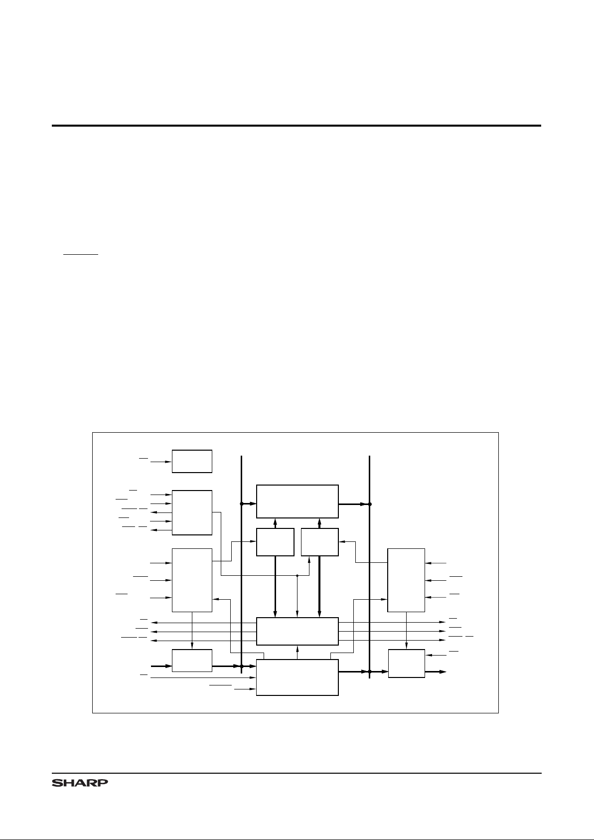
RESET
LOGIC
INPUT
PORT
RS
INPUT
PORT
CONTROL
LOGIC
READ
POINTER
WRITE
POINTER
DEDICATED AND
PROGRAMMABLE
STATUS FLAGS
FIFO
MEMORY ARRAY
512 x 18/1024 x 18
OUTPUT
PORT
CONTROL
LOGIC
FF
PAF
WXO/HF
RXO
/EF
2
PAE
D0 - D
17
WEN
WCK
Q
0
- Q
17
RCK
OUTPUT
PORT
REN
OE
PROGRAMMABLE
REGISTERS
EXPANSION
LOGIC
WXI/
WEN
2
FL/
RT
WXO/HF
RXI/
REN
2
RXO/
EF
2
LD
540215-1
WXI/
WEN
2
RXI/
REN
2
BOLD ITALIC = Enhanced Operating Mode.
EMODE
EF
Figure 1. LH540215/25 Bloc k Diagram
BOLD ITALIC = Enhanced Op erating Mode
1
Page 2

FUNCTIONAL DESCRIPTION
NOTE: Throughou t this data sheet , a
BOLD IT ALIC
type
font is used for all references to
Enhanced Operati ng
Mode
features which do not function in IDT-Compatible
Operating Mode; and also for all references to the
re-
transmit
facility (which is not an IDT72215B/25B FIFO
feature), even though it may be used – subject to some
restrictions – in either of these two operating modes.
Thus, readers interested only in using the LH540215/25
FIFOs in IDT -Com pat ib le Oper at ing M ode ma y skip over
BOLD IT ALI C
sections, if they wish.
The LH540215/25 parts a re FIFO (Fi rst-In, First-Out)
memory devices, based on fully-static CMOS dual-port
SRAM t ec h no logy, capabl e of containing up to 512 or 1024
18-bit words respectively. They can replace tw o o r mo re
byte-wide FIFOs in many appli cations, for mi croprocesso rto-microprocessor or microprocesso r-to-bus communication. Their architecture supports synchronous operation, tied
to two independent free-running clocks at the input and
output ports respectively . However, these ‘clocks’ also may
be a period ic, asyn chronou s ‘dem and’ sign als. Al most al l
control-input signals and status-output signals are synchronized to these clocks, to simplify system design.
The input and output ports operate altogether inde pendently of each ot her, un les s the FIFO becomes either
totally full or else totally empt y. Da ta flow is initiated at a
port by the rising edge of its cor responding clock , and is
gated by the appropr iat e edge-sam pled enab le signals.
The following FIFO status flags monitor the extent to
which the internal memory has been filled: Full, AlmostFull, Half-Full, Almos t-Empty , and Empty. The Almost-Full
and Almost-Em pty flag offsets are progr ammable over the
entire FI FO depth; but, during a reset operation, each of
these is initialized to a default offset value of 63
10
(LH540215) or 12710 (LH540225) F IFO-memory words,
from the respective FIFO boundary. If this default offset
value is satisf actor y, no further program ming is r equir ed.
After a reset operatio n during wh ich the
EMODE
control
input was not asserted (was HIGH), these F IFOs operate in
the IDT-Compatible Operating Mode. In thi s mode, each
part is pin-compatible and functionally-compatible with the
IDT72215B/25B part of similar depth and speed grade; and
the
Control Regis ter
is not even accessible or visible to the
external-sys tem logic whic h is contr olling the FIFO, althou gh
it still performs the same co nt rol functi o ns .
However, assertion of the EMODE control input
during a rese t ope rati on l eaves Contr ol Re gis ter bi ts
00-05 set, and causes the FIFO to operate in the
Enhanced Operating Mode. In essence, asserting
EMODE chooses a dif ferent default stat e for the Control Register. The system optionally then may program the Control Register in a ny desired manner to
activa te or deac tivate any or a ll of th e Enhanced -Operat ing-Mode features which i t can control, inc luding
sel ect able-cl ock -ed ge flag synchroni zation, and read
inhi bi tion w hen t he data output s ar e disabled.
Whenev er EMODE is being asserted, interlocke dopera tion paral leling also is avai lable, by appropriate
inter connect i on of the FIFO’s expansi on in puts .
The retransmit facility i s available during standalone
operation, in either IDT-Compatible O perating Mode or
Enhanced Operating Mode. (See Tables 1 and 2.) It is
ino per ativ e if t he FL/RT input signal is grounded . It is not
an IDT72215B/25B feature.
The Retransmit control
sign al causes the interna l FIFO read-address pointer
to be set back to zero, without affecting the internal
FIFO write-address pointer. Thus, the Retransmit
contr ol signal al so provi des a mechani sm whereby a
bloc k of dat a delimi ted by the zero physica l address
and the current writ e-address-pointer address may
be re ad out r epeat edl y , an ar bi trar y num ber of times .
The only restrictions are that neit her the read-address pointer nor the write-address pointer may
‘wra p around’ dur ing this entire pro cess, and that the
retransmit facili ty is not available during depth-cascaded oper ation, ei ther in IDT -Com pat ible Oper atin g
Mode o r in Enhanced Opera ting Mode. (See T abl es 1
and 2.) A lso, the flags behave differen tly for a short
time after a retransmit operation. Otherwis e, the retransm it facility is ava ilable du ring standa lone operation, in either IDT-Compatible Operating Mode or
Enh anced Oper ating M ode.
Note that, when FL/RT is being used as RT, RT is
an asser tive -HI GH signal , rather tha n asser tive -LOW
as it is in most other FIFOs having a retransmit
facility.
Progr am ming the progr am mable-flag of fs et s,
the t iming synchronization of the various status flags, the
optional read-suppression funct ionality of OE, and
the b ehavi or of the po inter s whic h access the of fset val ue regi st ers and th e Control Regis ter
may b e individually controlled by asserting the signal LD, without any
res et operat io n. When LD is being asserted, and writing
is being enabled by asserting WEN, some por tion of the
input b us word D0 – D17 is used at the next rising edge of
WCLK to program one or more of the programmable
regis ters on suc cessive write cloc ks. Likewise, the values
programmed into these programmable registers may be
read out for verification by asserting LD and REN, with
the outputs Q0 – Q17 enabled. Reading out thes e programm able register s should not be initiated while they are
being writ ten into. T able 3 defines t he possi ble mode s of
operation for loading and reading out the contents of
prog ramm able registe rs .
BOLD ITALIC = Enhanced Op erating Mode
LH540215/25 512 x 18/1024 x 18 Synchronous FIFO
2
Page 3
In the Enhanced Operat in g Mode, co ordi nat ed o peration of two 18-bit FIFOs as one 36- bit FIFO may be
ensured by ‘inter locked’ crosscoupl ing of the statusflag output s from each FI FO to the expansi on input s
of the other one; that is, FF to WXI/WEN2, and EF to
RX I/REN2, in both direct ions between tw o parallel ed
FIFOs. This ‘interlocked’ operation takes effect
automat ically, if two paral leled FIFOs are crossconnected in this manner, with t he EMO DE control input
being asserted (LOW). (See Tables 1 and 2, also
Figur es 27 and 30.) IDT -com pat ib le depth cascadi ng
no longer is available when operating in this ‘interlocked-paralleled’ mode; however, pipelined depth
cas cadi ng remai ns avai la ble .
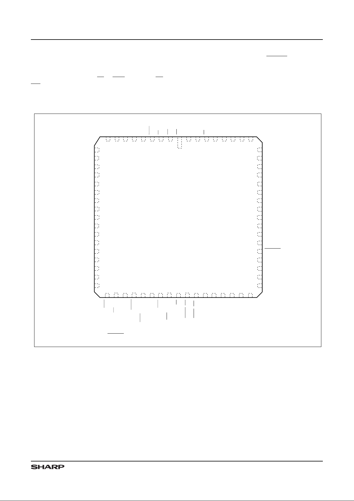
TOP VIEW
540215-2
3 2 1 6867666564636261987654
Q
17
Q
16
Q
15
LD
OE
V
CC
EF
V
CC
D15D16D
17
RCLK
REN
RS
16
17
18
19
20
23
24
21
22
26
15
11
12
13
14
10
25
D
2
D
0
D
13
D
14
D
11
D
12
D
9
D
10
D
8
V
CC
D
7
D
5
D
6
D
3
D
4
D
1
55
54
53
52
51
48
47
50
49
46
44
60
59
58
57
56
45
Q
11
V
CC
Q
10
Q
9
Q
8
Q
7
EMODE
*
Q
6
Q
5
Q
4
V
CC
Q
14
Q
13
Q
12
33 34 35 36 37 38 39 40 41 42 4327 28 29 30 31 32
Q2Q
3
WXO/HF
Q
0
Q
1
V
CC
V
CC
FL/
RT
WCLK
RXO/
EF
2
FF
RXI/
REN
2
PAF
WXI/
WEN
2
WEN
PAE
V
SS
V
SS
V
SS
V
SS
V
SS
V
SS
V
SS
V
SS
BOLD ITALIC = Enhanced Operating Mode.
*
This pin is VCC on IDT pinout; if EMODE pin is simply
biased to V
CC
, part will behave identical to IDT functionality.
68-PIN PLCC
Figure 2. Pin Connections for 68-Pin PLCC Package
BOLD ITALIC = Enhanced Op erating Mode
512 x 18/1024 x 18 Synchronous FIFO L H540215/25
3
Page 4
TOP VIEW
540215-34
58 57 56 55 54 53 52 51 50 4964 63 62 61 60 59
Q
17
Q
16
LD
OE
V
CC
EF
V
CC
D16D
17
REN
RS
7
8
9
10
11
14
15
12
13
6
2
3
4
5
1
16
D
2
D
0
D
13
D
15
D
11
D
12
D
9
D
10
D
8
D
7
D
5
D
6
D
3
D
4
D
1
RCLK
D
14
43
42
41
40
39
36
35
38
37
44
48
47
46
45
34
Q
14
Q
11
Q
12
Q
10
Q
9
Q
7
Q
8
Q
5
Q
6
Q
4
Q
13
33
Q
15
23 24 25 26 27 28 29 30 31 3217 18 19 20 21 22
Q
0
Q
1
PAF
FF
PAE
FL/
RT
WCLK
WXI/
WEN
2
WXO/HF
WEN
Q
2
V
CC
Q
3
64-PIN TQFP
V
CC
V
SS
V
SS
V
SS
V
SS
V
SS
EMODE
*
V
SS
RXO/
EF
2
RXI/
REN
2
V
SS
BOLD ITALIC = Enhanced Operating Mode.
*
This pin is VCC on IDT pinout; if EMODE pin is simply
biased to V
CC
, part will behave identical to IDT functionality.
Figur e 3. Pin Connect ion s for 64-Pi n TQFP Package
SUMMARY OF SIGNALS /PINS
PIN NAME
D0 – D
17
Data Inpu ts
RS Reset
EMODE Enhan ced Ope rati ng Mod e
WCLK Write Clock
WEN Write Enable
RCLK Read Cloc k
REN Read Enab le
OE Output Enable
LD Load
FL
/RT
First Load/
Retransmit
RXI
/REN
2
Read Expa nsio n Input/
Read Enable 2
PIN NAME
WXI
/WEN
2
Wri te Expa nsio n Input /
Write Enable 2
FF Full Flag
PAF Prog ramm abl e Almo st- Full Flag
WXO/HF Write Expansion Output/Half-Full Flag
PAE P rog ramm abl e Almo st- Empt y Fla g
EF Empty Flag
RXO/
EF
2
Read Expansion Output
/Empty Flag 2
Q0 – Q
17
Data Outputs
V
CC
Power
V
SS
Ground
BOLD ITALIC = Enhanced Op erating Mode
LH540215/25 512 x 18/1024 x 18 Synchronous FIFO
4
Page 5

PIN LIST
SIGNAL NAME PLCC PIN NO. TQFP PIN NO.
RS 1 57
OE 2 58
LD 3 59
REN 4 60
RCLK 5 61
D
17
763
D16864
D1591
D1410 2
D
13
11 3
D
12
12 4
D
11
13 5
D
10
14 6
D
9
15 7
D
8
17 8
D
7
19 9
D
6
20 10
D
5
21 11
D
4
22 12
D
3
23 13
D
2
24 14
D
1
25 15
D
0
26 16
PAE 27 17
FT/
RT
28 18
WCLK 29 19
WEN 30 20
WXI/
WEN
2
31 21
PAF 33 23
RXI/
REN
2
34 24
FF 35 25
WXO/HF 36 26
RXO/
EF
2
37 27
Q
0
38 28
SIGNAL NAM E PLCC PIN NO. TQFP PIN NO.
Q
1
39 29
Q
2
41 31
Q
3
42 32
Q
4
44 34
Q
5
46 36
Q
6
47 37
EMODE
48 33
Q
7
49 38
Q
8
50 39
Q
9
52 41
Q
10
53 42
Q
11
55 44
Q
12
56 45
Q
13
58 47
Q
14
59 48
Q
15
61 50
Q
16
63 52
Q
17
64 53
EF 66 54
V
SS
662
VCC16 NC
V
SS
18 NC
V
CC
32 22
V
SS
40 30
V
CC
43 NC
V
SS
45 35
V
SS
51 40
V
CC
54 43
V
SS
57 46
V
CC
60 49
V
SS
62 51
V
CC
65 NC
V
SS
67 55
V
CC
68 56
BOLD ITALIC = Enhanced Op erating Mode
512 x 18/1024 x 18 Synchronous FIFO L H540215/25
5
Page 6

PIN DESCRIPTIONS
PIN NAME
PIN
TYPE
1
DESCRIPTION
D0 – D
17
Data Inputs I Data inputs from an 18-bit bus.
RS Reset I
When
RS is taken LOW, the FIFO’s internal read and write pointers are set to
address the first physical location of the RAM array;
FF, PAF, and HF go HIGH;
and
PAE and EF go LOW . The pro gra mmab le- flag -of fs et regi ster s
and the
Control Register
are set to their default values. (But see the description of
EMODE
, below.) A reset operation is required before an initial read or write
operati on afte r power -up .
EMODE
Enhan ced
Opera tin g
Mode
I
When EMODE is tied LOW, the default setting for Control Register bits 00-05
after a reset operation changes to HIGH rather than LOW, thus enabling all
Control-Register-controllable Enhanced Operating Mode features, and
allowing access to the Control Register for reprogramming or readback.
(See Tables 1, 2, and 5.) If this behavior is desired,
EMODE may be
grounded; however, Control Register bits 00-05 still may be individually
program med to sel ecti vel y enabl e or disabl e certa in of the Enh ance d Mode
features, even though those features associated with interlocked-paralleled
operat ion alw ays are ena bled whenev er
EMODE is being asserted. (See
Table 2.) Alternatively,
EMODE may be tied to V
CC,
so that the FIFO is
functi onal ly IDT-co mpat ibl e, and the Con tro l Regis ter is not accessi ble or
visible, and all of its bits remain LOW.
Controlling EMODE dynamica lly
during system ope rati on is not recomme nded .
WCLK Write Clock I
Data is written into the FIFO on a LOW-to-HIGH transition of WCLK, whenever
WEN (Write Enable) is being asserted (LOW), and LD is HIGH. If LD is LOW, a
progra mmab le regi ster rathe r than the int erna l FIFO mem ory is writ ten into.
In the
Enhanced Operating Mode, WEN
2
is ANDed with WEN to produce an
effec tiv e inter nal wri te- enab le sign al.
2
WEN Write Enable I
When
WEN is LOW and LD is HIGH, an 18-bit data word is written into the FIFO
on every LOW-to-HIGH transition of WCLK. When
WEN is HIGH, the FIFO
internal memory continues to hold the previous data. (See Table 3.) Data will not
be written into the FIFO if
FF is LOW.
In the Enhanced Operating Mode, WEN
2
is ANDed wit h WEN to prod uce an effec tive intern al writ e-e nab le sign al.
2
RCLK Read Cloc k I
Data is read from the FIFO on a LOW-to-HIGH transition of RCLK whenever
REN
(Read Enable) is being asserted (LOW), and
LD is HIGH. If LD is LOW , a
progra mmab le regi ster rathe r than the int erna l FIFO mem ory is read from.
In the
Enhanced Operating Mode, REN
2
is ANDed with REN (and whenever
Contro l Regis ter bit 05 is HIGH, also wit h
OE) to prod uce an ef fect ive
internal read-enable signal.
2
REN Read Enab le I
When REN is LOW and LD is HIGH, an 18-bit data word is read from the FIFO on
every LOW-to-HIGH transition of RCLK. When
REN is HIGH, and/or also when
EF is LOW, the FIFO’s output register continues to hold the previous data word,
whether or not Q
0
– Q17 (the data outputs) are enabled. (See Table 3.)
In the
Enhanced Operating Mode, REN
2
is ANDed with REN (and whenever
Contro l Regis ter bit 05 is HIGH, also wit h
OE) to prod uce an ef fect ive
internal read-enable signal.
2
OE Output Enable I
When
OE is LOW, the FIFO’s data outputs drive the bus to which they are
connect ed. If
OE is HIGH, the FIFO’s outputs are in high-Z (high-impedance)
state.
In the Enhanced Operating Mode, OE not only continues to control the
outputs in this same manner, but also can function as an additional ANDing
input to the com bine d eff ect ive read -en able signal , alon g with
REN and
REN
2
, whenever Control Register bit 05 is HIGH. (See Table 5.)
2
1
I = Input, O = Output, Z = High-Impedance, V = Power Vo ltage Level
2
The ostensible differences in signal assertivenes s are reconciled before ANDing.
BOLD ITALIC = Enhanced Op erating Mode
LH540215/25 512 x 18/1024 x 18 Synchronous FIFO
6
Page 7

PIN DESCRIPTIO NS (cont’d)
PIN NAME
PIN
TYPE
1
DESCRIPTION
LD Load I
When
LD is LOW, the data word on D0 – D17 (the data input s) is writ ten int o a
programmable-flag-offset register,
or into the Control Register (when in the
Enhanced Operating Mode),
on the LOW-to-HIGH transition of WCLK, whenever
WEN is LOW. (See Table 3.) Also, when LD is LOW, a word is read to Q0 – Q17 (the
data outputs) from the offset registers
and/or the Contro l Regis ter (wh en in the
Enhanced Operating Mode)
on the LOW-to-HIGH transition of RCLK, whenever
REN is LOW. (See again Table 3, and particularly the Notes following this table.)
When
LD is HIGH, normal FIFO write and read operations are enabled.
FL
/RT
First Load /
Retran smit
I
In the standalone or paralleled configuration,
FL/RT should be LOW during a reset
operation. (See Tables 1 and 2.)
However, thereafter, in the standalone or
paralleled configuration, if
FL is taken HIGH, it functions instead as RT
(Retransmit), and resets the FIFO’s internal read pointer to the first physical
locati on of the RAM array . Note that alt hou gh Retr ans mit is an ‘en han ced’
feature, it is always available for a FIFO during standalone operation, whether
the FIFO is in IDT-Compatible Operating Mode or in Enhanced Operating
Mode; it is not regula ted eit her by the Contro l Regis ter or by the
EMODE
control input.
In IDT-compatible cascaded configuration, FL has an entirely
different function; it is grounded for the first FIFO device (the ‘master’ device or ‘firstload’ device), and is set to HIGH for all other FIFO devices in the daisy chain. Thus,
the
Retransmit
feature is not available for FIFOs operating in an IDT-compatible
cascaded configuration.
WXI
/WEN
2
Write
Expansion
Input/
Write
Enable 2
I
This signal is dual-purpose; its functionality is determined during a reset operation,
accordi ng to its own stat e, and also accord ing to the stat es of the thre e other
control inputs
RXI
/REN
2
, FL
/RT
, and
EMODE
. (See Tables 1 and 2.) In the
standal one or paralle led con figu rat ion,
WXI/
WEN
2
is grounded. In the cascaded
configuration,
WXI/
WEN
2
is connecte d to WXO (Write Expansion Output) of the
previous device, and functions as
WXI.
In the Enhanced Operating Mode,
WXI/WEN2 functio ns as a second write- ena ble sig nal , WEN2, which is ANDed
with
WEN to prod uce an ef fect ive intern al writ e-e nabl e sign al.
2
RXI
/REN
2
Read
Expansi on
Input/
Read
Enable 2
I
This signal is dual-purpose; its functionality is determined during a reset operation,
accordi ng to its own stat e, and also accord ing to the stat es of the thre e other
control inputs
WXI
/WEN
2
, FL
/RT
, and
EMODE
. (See Tables 1 and 2.) In the
standal one or paralle led con figu rat ion,
RXI/
REN
2
is grounded. In the cascaded
configuration,
RXI/
REN
2
is connecte d to RXO (Read Expansion Output) of the
previous device, and functions as
RXI.
In the Enhanced Operating Mode,
RXI/REN2 functions as a second read-enable signal, REN2, which is AND ed
with
REN – and perhaps also with OE, if Cont rol -Reg ist er bit 05 is HIGH – to
produce an effective internal read-enable signal.
2
FF Full Flag O
When
FF is LOW, the FIFO is full; further advancement of its internal write-address
pointer, and further data writes through its Data Inputs into its internal memory
array, are inhibited. Whe n
FF is HIGH, the FIFO is not full. FF is synch ron ized to
WCLK.
PAF
Progra mmab le
Almost-Full Flag
O
When
PAF is LOW, the FIFO is ‘almost full,’ based on the almost-full-offset value
programmed into the FIFO’s Almost-Full Offset Register. The default value of this
offset at reset is one-eighth of the total number of words in the FIFO-memory array,
minus one, measured from ‘full.’ (See Table 4.) In the IDT-Compatible Operating
Mode,
PAF is asynchronous.
In the Enhance d Opera tin g Mode, P AF is
synchronized to WCLK after a reset operation, according to the state of
Control Register bit 04. (See Table 5.)
NOTES:
1. I = Input, O = Output, Z = High-Impedance, V = Power Voltage Level
2. The ostensib le differences in sign al assertiveness are reconciled before ANDing.
BOLD ITALIC = Enhanced Op erating Mode
512 x 18/1024 x 18 Synchronous FIFO L H540215/25
7
Page 8

PIN NAME
PIN
TYPE
1
DESCRIPTION
WXO/HF
Write
Expansion
Output/
Half-Full Flag
O
This signal is dual-purpose; its functionality is determined during a reset operation
according to the states of the two control inputs
WXI/
WEN
2
and RXI/
REN
2
. (See
T a bles 1 and 2.) In the standal one or para llel ed conf igur ati on, when ever
HF is LOW
the device is more than half full. In IDT-Compatible Operating Mode,
HF is
asynchronous;
in the Enhanced Operating Mode, HF may be synchronized
either to WCLK or to RCLK after a reset operation, according to the state of
Control Register bits 02 and 03. (See Table 5.)
In the IDT-compatible cascaded
configuration, a pulse is sent from
WXO to the WXI input of the next FIFO in the
daisy-chain cascade, whenever the last location in the FIFO is written.
PAE
Programmable
Almost-Empty
Flag
O
When PAE is LOW, the FIFO is ‘almost empty,’ based on the almo st- empt y-o ff set
value programmed into the FIFO’s Almost-Empty Offset Register. The default value
of this offset at reset is one-eighth of the total number of words in the FIFO-memory
array, minus one, measured from ‘empty.’ (See Table 4.) In IDT-Compatible
Operati ng Mode ,
P AE is async hro nous .
In the Enhanced Operating Mode, PAE
is synchron ize d to RCLK afte r a reset oper ati on, acc ordi ng to the sta te of
Control Register bit 01. (See Table 5.)
EF Empty Flag O
When
EF is LOW, the FIFO is empty; further advancement of its internal readaddress pointer, and further readout of data words from its internal memory array to
its Data Outputs, are inhibited. When
EF is HIGH, the FIFO is not empty. EF is
synchronized to RCLK.
RXO
/EF
2
Read
Expansion
Output
O
This signal is dual-purpose; its functionality is determined by the state of the
EMODE
control input during a reset operation. (See Tables 1 and 2.) In the IDT-
Compatible Operating Mode, in a cascaded configuration, a pulse is sent from
RXO
to the
RXI input of the next FIFO in the daisy-chain cascade, whenever the last
location of the FIFO is read.
In the Enhanced Operating Mode, whenever
EMODE is being asserted (LOW), EF2 behaves as an exact duplicate of EF,
but delayed by one full cycle of RCLK with respect to
EF.
Q0 – Q
17
Data Outputs O/Z Data outputs to drive an 18-bit bus.
V
CC
Power V +5 V power-supply pins.
V
SS
Ground V 0 V ground pins.
NOTE:
1. I = Input, O = Output, Z = High-Impedance, V = Power Voltage Level
PIN DESCRIPTIONS (cont’d)
BOLD ITALIC = Enhanced Op erating Mode
LH540215/25 512 x 18/1024 x 18 Synchronous FIFO
8
Page 9
ABSOLUTE MAXIMUM RATINGS
PARAMETER RATING
Supply Voltage to VSS Potentia l –0.5 V to 7 V
Signal Pin Voltage to V
SS
Potenti al –0.5 V to VCC + 0.5 V
DC Output Current
1
±75 mA
Temperature Range wit h Powe r Appli ed
2
–55°C to 125°C
Stora ge Temperatur e Rang e –65°C to 150°C
Power Dissipation (PLCC Package Limit) 2 W
NOTES:
1. O nly one out put may be shorted at a time, for a period not exceed ing 30 seconds.
2. Measured with clocks idle.
OPERATING RANGE
SYMBOL PARAMETER MIN. MAX. UNIT
T
A
T emper ature, Amb ient
070C
V
CC
Supply Voltage 4.5 5.5 V
V
SS
Supply Voltage 0 0 V
V
IL
Logic LOW Input Voltage –0.5 0.8 V
V
IH
Logic HIGH Input Voltage 2.0 VCC + 0.5 V
DC ELECTRICAL CHARACTERISTICS (Over Operating Range)
SYMBOL PARAMETER TEST CONDITIONS MIN. MAX. UNIT
I
LI
Input Leakage VCC = 5.5 V, VIN = 0 V to V
CC
–10 10 µA
I
LO
I/O Leakage OE ≥ VIH, 0 V ≤ V
OUT
≤ V
CC
–10 10
µA
V
OH
Output HIGH Vo ltag e IOH = –12.0 mA 2.4 V
V
OL
Output LOW V ol tage IOL = 16.0 mA 0.4 V
I
CC
Average Operating Supply Current
1
Measur ed at fCC = 50 MHz 190 mA
I
CC2
Average Standby Supply Current All inputs = V
IH
MIN. (cl ocks idle) 25 mA
I
CC3
Power-Down Supply Current All inputs = VCC – 0.2 V (clocks idle) 1 mA
NOTE:
1. Output load is disconnected.
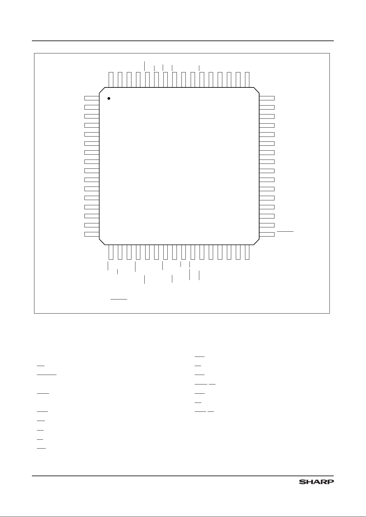
AC TE ST C O N DIT IO N S
PARAMETER RATING
Input Puls e Levels VSS to 3 V
Input Rise and Fall T ime s
(10% to 90%)
3 ns
Input T imi ng Refe renc e Level s 1.5 V
Output Tim ing Ref ere nce Leve ls 1.5 V
Output Load,
Tim ing Tests
(Figure 4)
R
1
(Top Resistor ) 1.1k Ω
R
2
(Bottom Resist or)
680 Ω
C
L
(Load Capacitance) 30 pF
CAPACITANCE
1, 2
PARAMETER RATING
CIN (Input Capacitance) VIN = 0 V 8 pF
C
OUT
(Output Capaci tanc e) V
OUT
= 0 V 8 pF
NOTES:
1. Sample tested onl y.
2. Capacitances are maximum values at 25°C, measured at
1.0 MHz, with V
IN
= 0 V.
540215-3
DEVICE
UNDER
TEST
+5 V
30 pF
1.1 k Ω
680 Ω
INCLUDES JIG AND SCOPE CAPACITANCES
*
*
Figure 4. Output Load Circuit
BOLD ITALIC = Enhanced Op erating Mode
512 x 18/1024 x 18 Synchronous FIFO L H540215/25
9
Page 10

AC ELECTRICAL CHARACTERISTICS
SYMBOL PARAMETER
–20 –25 -35
MIN. MAX. MIN. MAX. MIN. MAX.
f
CC
Clock Cycle Frequency 50 40 28.6
t
A
Data A cces s T ime 2 12 3 15 3 20
t
CLK
Clock Cycle Time 20 25 35
t
CLKH
Clock HIGH Time 8 10 14
t
CLKL
Clock LOW Time 8 10 14
t
DS
Data Set up T ime 5 6 7
t
DH
Data Hol d Ti me 2 2 2
t
ENS
Enable Setup Time 5 6 7
t
ENH
Enable Hold Time 2 2 2
t
RS
Reset Pulse Width
1
20 25 35
t
RSS
Reset Setup Time
2
12 15 20
t
RSR
Reset Recovery Time
2
12 15 20
t
RSF
Reset to Flag and Output Time 30 35 40
t
OLZ
Output Enable to Output in Low-Z
2
000
t
OE
Output Enable to Output Valid 9 12 15
t
OHZ
Output Enable to Output in High-Z
2
19112115
t
WFF
Write Clock to Full Flag 12 15 20
t
REF
Read Clock to Empty Flag 12 15 20
t
PAF
Clock to Programmable Almost-Full Flag (IDT-Compatible Operating
Mode)
14 17 23
t
PAE
Clock to Programmable Almost-Empty Flag (IDT-Compatible
Operating Mode)
14 17 23
t
HF
Clock to Half-Fu ll Flag (IDT - Comp ati ble Oper ati ng Mode ) 14 17 23
t
PAFS
Clock to Programmable Almost-Full Flag
(Enhanced Operating Mode)
14 17 23
t
PAES
Clock to Programmable Almost-Empty Flag
(Enhanced Operating Mode)
14 17 23
t
HFS
Clock to Half-Full Flag (Enhanced Operating Mode) 14 17 23
t
XO
Clock to Expansion-Out 12 15 20
t
XI
Expan sion -In Pul se Width 7 9 13
t
XIS
Expan sion -In Set up T ime 7 9 14
t
SKEW1
Skew Time Between Read Clock and Write Clock for Full Flag
3
91116
t
SKEW2
Skew T ime Bet ween Write Clock and Read Clock for Emp ty Flag
4
91116
NOTES:
1. Pulse widths less than the stated minimum values may cause incorrect oper ation.
2. Values are guaranteed by design; not c urrently tested.
3. These times also apply to the Programmable-Almost-Full and Half-Full flags when they are synchronized to WCLK.
4. These times also apply to the Half-Full and Prog rammable-Almost-Empty flags when they are synchronized to RCLK.
BOLD ITALIC = Enhanced Op erating Mode
LH540215/25 512 x 18/1024 x 18 Synchronous FIFO
10
Page 11

DESCRIPTION OF SIGNALS AN D
OPERATING SEQUENCES
T abl e 1. Gro upin g-Mode Det erm inatio n
During a Reset Oper ation
5
EMODE
WXI/
WEN
2
RXI/
REN
2
FL/
RT
MODE
WXO/HF
USAGE
WXI/
WEN
2
USAGE
RXI/
REN
2
USAGE
FL/
RT
USAGE
RXO
/EF
2
USAGE
H
1
HHH
Cascaded
Slave
2
WXO WXI RXI FL RXO
H
1
HHL
Cascaded
Master
2
WXO WXI RXI FL RXO
H
HLX
(Reser ved)
–––––
H
LHX
(Reser ved) –––––
H
LL H
3
(Not Allowed
During Reset )
(HF) (no ne) (none)
(RT)
(none)
H
LL L
3
Standalone HF (none) (none)
RT
(none)
LXX
H
3
(Not Allowed
During Reset)
(HF) (WEN2) (REN2) (RT) (EF2)
LXX
L
3
Interlocked
Paralleled
4
HF WEN
2
REN
2
RT EF
2
NOTES:
1. In IDT-compatible cascading, a reset operation forces
WXO/HF and RXO/
EF2
HIGH for the nth FIFO, thus forcing WXI/
WEN2
and RXI/
RE N
2
HIGH for the (n + 1)st FIFO.
2. The terms ‘master’ and ‘slave’ refer to IDT-compatible casca ding . In pipelined casca ding4, there is no such distinction.
3. Once grouping mode has been determined during a reset operation, FL/RT then may go HIGH to activate a retransmit operation.
4. EMODE must be asserted for access to the Control Register to be enabled. Also, FIFOs being used in a pipelined-cascading
configuration should be in Interlocked Paralleled mode.
5. Setup-time and recovery-time specifications apply during a reset operation.
6. H = HIGH; L = LOW; X = Don’t Care.
T abl e 2. Expansi on- Pin Usage According to
Groupi ng Mo de
I/O PIN
IDT-COMPATIBLE OPERA TING MODE
ENHAN CED
OPER ATING MODE
DEPTH-CASCA DED
MASTER
DEPTH-CASCADED
SLAVE
STANDALONE
INTERLOCKED
PARALLELED
I WXI /
WEN
2
From WXO ((n-1)st FIFO) From WXO ((n-1)st FIFO) Grounded
From FF (other FIFO)
O WXO/HF To WXI ((n+1)st FIFO) To WXI ((n+1)st FIFO) Becomes HF
Becomes HF
I
RXI/
REN
2
From RXO ((n-1)st FIFO) From RXO ((n-1)st FIFO) Grounded
From EF (other FIFO)
O RXO
/EF
2
To RXI ((n+1)st FIFO) To RXI ((n+1)st FIFO) Unused
Becomes EF
2
I FL/
RT
Grounded (Logic LOW) Logic HIGH
Becomes RT1Becomes RT
1
NOTE:
1.
FL/RT may be grounded if
the Retransmit fa cility
is not being used.
BOLD ITALIC = Enhanced Op erating Mode
512 x 18/1024 x 18 Synchronous FIFO L H540215/25
11
Page 12

T abl e 3. Select ion of Re ad and Wri te Oper ati ons
LD WEN
3,4
REN
3, 4
WCLK RCLK ACTION
LXX– –
No operation.
LLL
∧∧
Illegal combination, which will cause errors.
LLH
∧
X Write to a programmable register.
1
LHH ∧ X
Hold present value of programmable-register write counter, and do not
write.
2
LH L X ∧Read from a programmable register.
1
LHHX
∧
Hold present value of programmable-register read counter, and do not
read.
2
HL X
∧
X Normal FIFO write operation.
HXLX
∧
Normal FIFO read operation.
H L X – X No write operation.
HHXXX
No write operation.
H X L X – No read operation.
H X H X X No read operation.
H L L – – No operation.
KEY:
H = Logic ‘HIGH’; L = Logic ‘LOW’; X = ‘Don’t-care’ (logic ‘HIGH,’ logic ‘LOW,’ or any transition);
∧ = A ‘LOW’-to-‘HIGH’ transition; – = Any condition EXCEPT a ‘LOW’-to-‘H IGH’ transition.
NOTES:
1. The selection of a programmable register to be written or read is controlled by two simple s tate machines. One state machine controls the selection for writing; the other state machine controls the selection for reading. These two state machines operate independently of each other.
Both state machines are reset to point to Word 0 by a reset operation.
In the Enhanced Operating Mode, if Control Register bit 00 is set,
both state machines are al s o reset to point to Word 0 by deassertion of LD after LD has been asserted (that is, by a rising edge of
LD), followed by a valid memory array write cycle for the writing-control state machine and/or by a valid memory array read cycle
for the reading-control state machine.
2. The order of the two programmable registers which are accessible in IDT-Compatible Operating Mode, as selected by either state machine, is
always:
Word 0: Almost-Empty Offset Register
Word 1: Almost-F ull O f fse t Regi ster
Word 0: Almost-Empty Offset Register
...
(repeats indefinitely)
...
The order of the three programmable registers which are accessible in Enhanced Operating Mode, as selected by either state
machine , is al ways:
Word 0: Almo s t-Empty Offset Reg ist er
Wo rd 1: Almost-Full Offset Register
Wo rd 2 : Control Register
Wo rd 0: Almost-Empty Offset Register
………
…
(repeats indefinitely)
………
…
Note that, in IDT-Compatible Operating Mode, Word 2 is not accessed; Word 0 and Word 1 alternate.
3. After normal FIFO operation has begun, writing new contents into either of the offset re gisters should onl y be done when the FIFO is empty .
4. WEN2, REN2, and OE may be ANDed terms in the enabling of read and write operations, accordi ng to the state of the EMODE control
input and of Control Register Bit 05.
BOLD ITALIC = Enhanced Op erating Mode
LH540215/25 512 x 18/1024 x 18 Synchronous FIFO
12
Page 13

T abl e 4. Status Flags
NUMBER OF UNRE AD DATA WORDS PRE SENT WITHIN FIFO
1, 2
FULL
FLAG
MIDDLE FLAGS
EMPTY
FLAG
512 × 18 FIFO 1024 × 18 FIFO
FF PAF HF PAE EF
0 0 HHHLL
1 to q 1 to q H H H L H
(q + 1) to 256 (q + 1) to 512 HHHHH
257 to (512 – (p + 1)) 513 to (1024 – (p + 1)) H H L H H
(512 – p) to 511 (1024 – p) to 1023 H L L H H
512 1024 L L L H H
NOTES:
1. q = Programmable-Almost-Empty Offset value. (Default values: 512 × 18, q = 63; 1024 × 18, q = 127.)
2. p = Programmable-Almost-Full Offset value. (Default values: 512 × 18, p = 63; 1024 × 18, p = 127.)
3. Only 9 (51 2 × 18) or 10 (1024 × 18) of the 12 offset-value-register bits should be programmed. The unneeded most-signi ficant-end bits sh oul d
be LO W (zero).
4. The f lag outp ut is delayed by one full clock cyc le in Enhanced Operating Mode, when synchronous operation is specified fo r intermediate flags.
DESCRIPTION OF SIGNAL S AND OPERA T I NG SEQUENCES (con t’d)
BOLD ITALIC = Enhanced Op erating Mode
512 x 18/1024 x 18 Synchronous FIFO L H540215/25
13
Page 14

Tabl e 5. Control-Regi st er Form at
COMMAND
REGISTER
BITS
CODE
VALUE AFTER RES E T FLAG
AFFECTED,
IF ANY
DESCRIPTION NOTES
EMODE = H EMODE = L
00
L
LH–
Deassertion of
LD does not
reset the pro gram mabl eregister write pointer and
read pointer.
IDT - comp ati ble add ress ing
of programmable registers.
H
Deassertion of
LD resets
the programmable-register
write pointer and read
pointer to address Word 0,
the Programmable-AlmostEmpty- Flag -Of fs et Regi ste r .
The change takes effect
after a valid write ope rati on
or a valid read operation,
respect ive ly , to the memo ry
array .
Non-a mbi guou s
addressing of
programmable registers.
01
L
LH
PAE
Set by
↑↑
RCLK, reset by
↑↑
WCLK.
Asynchronous flag
clocking.
H
Set and reset by
↑↑
RCLK.
Synch rono us fla g clock ing.
03, 02
LL
LL HH HF
Set by
↑↑
WCLK, reset by
↑↑
RCLK.
Asynchronous flag
clocking.
LH Set and reset by
↑↑
RCLK.
Synch rono us fla g clock ing
at output port.
HL,
Set and reset by
↑↑
WCLK.
Synch rono us fla g clock ing
at input port.
HH
04
L
L
H
PAF
Set by
↑↑
WCLK, reset by
↑↑
RCLK.
Asynchronous flag
clocking.
H
Set and reset by
↑↑
WCLK.
Synch rono us fla g clock ing.
05
L
LH–
OE has no effect on an
intern al read operat ion ,
apart from disabling the
outputs.
Allows the read-address
point er to adva nce eve n
when Q
0
– Q17 are not
driving the output bus.
H
Deassertion of
OE inhibits
a read operation; whenever
the data outputs Q
0
– Q
17
are in the high-Z state, the
read pointer does not
advance.
Inhibits the read-address
point er fro m advanc ing
when Q
0
– Q17 are not
driving the output bus;
thus, guards against data
loss.
06
L
LL
–
Reserved.
Future use to control depth
cascading and interlocked
paralleling.
H
11, 10,
09, 08, 07
LLLLL LLLLL LLLLL
–
Reserved. Reserved.
NOTES:
1.
When
EMODE
is HIGH, and
Control Register bits 00-05 are LOW,
the FIFO behaves in a manner functionally equiv alent to the
IDT72215B/25B FIFO of similar depth and speed grade. Under these conditions, the
Control Register
is not visible or accessible to the ex-
ter nal syst em whi ch inclu des t he FIFO.
2.
If
EMODE
is not asserted (is HIGH),
Control Register bits 00-05 remain LOW
after a reset operation.
Howeve r, if EMODE is asserted (is
LOW) during a reset operation, Control Register bits 00-05 are forced HIGH, and remain HIGH until cha nged. Control Register bits
06-11 are unaffected by EMODE .
BOLD ITALIC = Enhanced Op erating Mode
LH540215/25 512 x 18/1024 x 18 Synchronous FIFO
14
Page 15

Data Inputs
DATA IN (D0 – D17)
Data, progra mmable-flag-offset values, and
Control-
Register
codes are input to the FIFO as 18-bit words on
D0 – D17. Unused bit positions in offset-v alue
and Con-
trol-Register
words should be zero-filled.
Control Inputs
RESET (RS)
The FIFO is reset whenever the asynchro nous Reset
(RS) input is taken to a LOW state. A reset operation is
required after power-up, be fore the first write operation
may occur. The state of the FIFO is fully defined after a
reset operation. If the default values which are entered
into the Progra mmable-Fl ag-Offset-Value Registers
and
the Control Register
by a reset operation are acceptable, then no device programming is required. A reset
operat ion init ializes the FIFO’s internal read-add ress and
write-a ddress point ers to the FIFO’s f irst physical memory
location. The five sta tus flags, FF, PA F, HF, PA E, and EF,
are updated to indicate that the FIFO is completely empty;
thus, the first three of these are reset to HIGH, and the
last two are re set to LOW . The f lag -of fse t values for PAF
and P A E each are init ialize d to one- eight h of th e de pth of
a single FIFO, minus one; 63 for a 512-word FIF O, and
127 for a 1024-word FIFO. If
EMODE
is not being as-
sert ed (i.e. , if
EMOD E
is HIGH), all
Contro l Register
bits
are initialized to LOW, to configur e the FIFO to opera te in
the IDT72215B/ 25B-Compati ble Opera ting Mode. Unt il a
write opera tion occu rs, the data output s D0 – D17 all are
LOW whenever OE is LOW.
ENHANCED OPERATING MODE (EMODE)
Whenever EMODE is asserted during a reset operation, Contr ol Register bits 00 – 05 re main HIGH
rather than LOW after the completion of the reset
operation. Thus, EMOD E has the effe ct of act iva tin g
all of the Enhanced- Opera ting- Mod e featur es durin g
a reset operation. Subsequently, they may be individual ly disabl ed or re-enabl ed by changing the set ting of Control-Regis ter bi ts. The behavior of these
Enhanced-Opera ting-Mode features is described in
Table 5. For permanent Enhanced-Operating-Mode
operation, EMODE must be grounded; dy nami c c ontrol of EM OD E during sys tem oper ation is not recom mended.
Asser ting EMODE during a reset operation also
causes WXI/WEN2 to be configured as WEN2, and
RX I/REN2 to be conf igured as RE N2, to support interlocked-paralleled operation of two FIFOs ‘side by
side. (See Figur e 27.) Additional ly , RXO/EF2 is conf igured as EF2, which dupl icate s the EF signal with one
extra RCK cycle delay, in order to provide proper
timing for ‘pipelined’ cascaded opera tion.
WRITE CLOCK (WCLK)
A rising ed ge (LO W-to-HIGH transition) of WCLK in iti ates a FIFO w rite cycle if LD is HIGH, or a programmable-re giste r write cycle if LD is LO W . The 18 da ta inputs,
and a ll input-side synchronous control inputs, mus t meet
setup and hold times with respect to the rising edge of
WCLK. The input-side sta tus flags are meaningful after
specified time interva ls, following a rising edge of WCLK.
Conceptua lly, the WCLK input r eceives a free-running ,
periodic ‘clock’ waveform, which is used to control other
signals which are edg e-sensit ive. Howeve r, th ere actually
is not any abso lute requirem ent t hat the W CLK wavef orm
must
be periodic. An ‘asynchronous’ mode of operation
is in fact possible, i f WEN is continuously asserted (that
is, is continuously held LOW), and WCLK receives aperiodic ‘cloc k’ pulses of suitable duration . There like wise is
no requirement that WCLK must have any particular
synchronization relation to the read clock RCLK. These
two clock inputs may in fact receive the same ‘clock’
signal; or t hey m ay r eceive totally-diffe rent signa ls, which
are not synchron ized to each other in any way.
WRITE ENABLE (WEN)
Whenever WE N is being asser t ed (is LO W) an d LD is
HIGH, and the FIF O is not ful l, an 18-bit data word is
loaded into the effective inpu t register for the memory
array at every WCLK rising edge (LOW-to-HIGH transition ). Data words are s tored into the two-port memory
array sequ entia lly , regard less of any ongoing re ad oper ation. Whenever W EN is not being asserted (is HI GH), the
input register retains whatever data word it contained
previousl y, and no new data word gets loaded into the
memo ry arr ay.
To preve nt overrunning the internal FIFO boundaries,
further write operati ons are inhi bited whenever t he Full
Flag (FF) is being asserted (is LOW). If a valid read
oper a tion then occurs, upon the completion of that read
cycle FF again goes HIGH after a time t
WFF
, and another
write operation is allowed to begin whenever WCLK
makes another LOW-to-HIGH transition. Effectively,
WEN is overridden by FF; thus, during normal FIFO
operation, WEN has no effect when the FIFO is full.
In the Enhanced Operating Mode, whenever
EMOD E is being asserted (is LOW), WXI/ W E N2 functions as WEN2, an additiona l duplicate (albei t assertive-HIGH) write-enable input, in order to provide
an‘interlocking’ mechanism for reliable synchronization of two paral leled FIFOs. To control writing ,
WEN2 is ANDed with WEN; this logic-AND function
(WEN
WEN2) then behaves l i ke W EN i n the forego-
ing descr iption.
DESCRIPT ION OF SIGNAL S AN D
OPERATING SEQUENCES (cont’d )
BOLD ITALIC = Enhanced Op erating Mode
512 x 18/1024 x 18 Synchronous FIFO L H540215/25
15
Page 16

READ CLOCK (RCLK)
A rising edge (LOW- to-HI GH transition) of RCLK initiates a FIFO read cycle if LD is HIGH, or a programmable-register read cycle if LD is LOW. All output-side
synchronous control inpu ts must meet setup and hold
times with respect to the risin g edge of RCLK. The 18 d ata
output s, and the out put- side st atus fla gs, are mea ningf ul
after specified time intervals, following a rising edge of
RCLK.
Conceptu ally , the RCLK input receives a free-run ning,
periodic ‘clock’ waveform, which is used to control other
signals which are edge-sensitive . However, there actually
is not any absolute require ment that the RCLK waveform
must
be periodic. An ‘asynchr onous’ mode o f operation is
in fact possible, if REN is continuously asser ted (that is,
is continuously held LOW) , and RCLK receives aperiod ic
‘clock’ pulses of suitable duration. There likewise is no
requirement that RCLK must have any particular s ynchronization relation to the write clock WCLK. These two clock
inputs may in fact receive t he sam e ‘cloc k’ signal; or they
may receive totally-different signals, which are not synchronized to each other in any way .
READ ENABLE (REN)
Whenever REN is being asserted (is LOW), and the
FIFO is not empty, an 18-bit data word is loaded int o the
output register f rom the memory array at every RCLK
rising edge (LOW-to-HIGH transition). Data words are
read from the two-port memory array sequentially , regardless of any o ngoing writ e opera tion. Whenever REN is not
being asserted (is HIGH), the output register retains
whatever data word it contained previously, and no new
data word gets loaded into it from the memory array .
T o prevent underru nning the internal FIFO boundaries,
further re ad operations ar e inhibited whenever the Emp ty
Flag (EF) is being asserted (is LOW). If a vali d write
operation then occurs, upon the completion of that write
cycle EF again goes HIGH af ter a time t
REF
, and anot her
read operation is allowed to begin whenever RCLK
makes a nother LOW-t o-HIGH t ransition. Effect ively , REN
is overridden by EF; t hus, during normal FI FO operation,
REN has no ef fect when the FIFO is empty.
In the Enhanced Operating Mode, one (o r, sometimes two) additional read-enable inputs may be
ANDed w ith REN to control reading, depending on
the state of Contr ol-R egister Bit 05. The additional
read-enable input(s) are REN2 (and OE) .
Whenever EMODE is being asserted (is LOW),
RXI/REN2 functi o n s as REN2, an additi onal duplicate
(albe it assert ive-HIG H) Rea d-Enable input, i n or der to
provide an ‘interlocking’ mechanism for reliable
synchroni zati on of two parallele d FIFOs.
Also, i f Cont rol Register bit 05 has been set, OE
takes on the extra role of serving as yet another
duplicate read-enable input, in addition to its usual
function of controlling the FIFO’s data outputs, in
order to inhi bit f urt her read operations w henev er the
FIFO’s data outputs are disabled, and thereby to
preve nt dat a loss under some circ umst ance s.
OUTPUT ENABLE (OE)
OE is an assertive-LOW, asynchronous, output
enable. In the IDT-Compatible Operati ng Mode, OE has
only the effect of enabling or disabl ing the data outputs
Q0 – Q17. That is, disabling Q0 – Q17 does not inhibit a
read operation, for data being transmitted to the output
register; the same data will remain available later, when
the outputs are again enabled, unless subsequently over written. When Q0 – Q17 are enabled, each of these 18
dat a output s is in a norm al HIGH or LOW state , according
to the bit pattern of the data word in the output register.
When Q0 – Q17 are disabled, each of these output s is in
the high-Z (high-impedance) state.
In the Enhanced Oper ating Mode, if Control Register bit 05 has been set, OE behaves as an additional
read-enable control input, as well as enabling and
disabling the data outputs Q0 – Q17. Under these
circumstances, incrementing the read-address
pointer is inhibited whenever Q0 – Q17 are in the
high- Z st ate. Thus, ‘ readi ng’ success ive w ords which
fail ever to reach the outputs is prevented, as a
safe guar d again st data loss.
LOAD (LD)
The Sharp LH540215/25 FIFOs contain
three
18-bit
programmable registers. The contents of these three
regist ers may be loaded with data from the data inputs
D0 – D17, or read out onto the da ta outp uts Q0 – Q17. The
first two registers are the Programmable-Flag-OffsetValue Registers, for the Programmable Al most-Empty
Flag (PAE) and the Progr ammab le Almost-F ull Flag (PAF)
res pectiv ely .
The third register is the Control Regist er ,
which includes several configuration-control bits
for selectively enabling and disabling Sharp’s
Enhanced-Operating-Mode features.
None o f these three registers makes use of all of its
available 18 bits . Figure 5 shows which bit positions of
each register are operational. The two ProgrammableFlag-Of f set- Value Registe rs each c ont ain an offs et value
in bits 0-8 (LH540215) or bits 0 – 9 (LH5402 25); bits 9 –
17 (LH540215) or bits 10 – 17 (LH540225) are unused.
The default values for both offsets are one-eighth of the
total number of words in the FIF O memory array, minus
one: 63 for a 512 × 18 FIFO, and 127 for a 1024 × 18
FIFO.
BOLD ITALIC = Enhanced Op erating Mode
LH540215/25 512 x 18/1024 x 18 Synchronous FIFO
16
Page 17

The
Contr ol Register
configuration is shown in Fig-
ure 5 and in Table 5. For the
Control Regis ter
, in the
IDT-Compatible Operating Mode, with
EMODE
deasserte d (HIGH), the default value for all Control-Regist e r
bits is zero (LOW).
In the Enhanced Operating Mode,
with E MODE asserted (LOW ), the defau lt value for
bits 00-05 i s HIGH, and the def ault va lue for bits 06- 1 1
is LOW.
Whenever LD and WEN are simultaneously being
asserted (are both LOW ), the 18-bit d ata word from the
data inputs D0 – D17 is written into the Programmabl e-
Almost-Empty-Flag -Offset-Value Register at the first rising edge (LOW-to-HIGH transition) of the write clock
(WCLK). (See Table 3.) If LD a nd WEN continue to be
simultaneously asserted, another 18-bit data word from
the data inputs D0 – D17 is written into the Programmable-A lmost-Full-Flag -Offset-V alue Register at the second
rising edge of WCLK.
What happens next is de termined by the stat e of the
EMODE
control input. If it is dea sserted (HIG H) , th e next
18-bit word from the data inputs D0 – D17 is writ te n back
into the Programmable-Almost-Empty-Flag- Offset-Value
Register again.
540215-4
PROGRAMMABLE-ALMOST-EMPTY-FLAG-OFFSET VALUE
1, 2
091017
017
PROGRAMMABLE-ALMOST-FULL-FLAG-OFFSET VALUE
1, 2
WORD 0
CONTROL REGISTER
4, 5
12345617
WORD 1
WORD 2
5
2
3
Future use to control depth cascading and interlocked paralleling.
Enables suppressing reading whenever data outputs are disabled.
Makes PAF synchronous.
Makes HF synchronous. (See the Control-Register Format
table for the encoding of bits 02-03.)
Makes PAE synchronous.
Selects reinitialized addressing of the programmable registers.
6
5
3
6
BOLD ITALIC = Enhanced Operating Mode.
1 0
= Reserved. Do not load with non-zero information.
1
0
2
011
4
CONTROL-REGISTER BITS:
4
Reserved for
future use.
12 7
8
3
3
NOTES:
1. Default offset values are 63
10
= 3F
16
(LH540215) or 127
10
= 7F16 (LH540225).
2. Bits 9-17 (LH540215) or bits 10-17 (LH540225) of both offset-value registers should
in all cases be programmed LOW (zero).
3. This bit position is used for offset values in the LH540225 only. In the LH540215, it
always should be programmed LOW.
4. See the Control-Register Format table for the default states of the Control Register,
for EMODE = HIGH (IDT-Compatible Operating Mode) and for EMODE = LOW (Enhanced Operating Mode).
The Control Register is not accessible or visible in IDT-Compatible Operating Mode.
5. The assertion of EMODE (LOW) forces Control Register bits 00-05 HIGH during a reset operation.
After that, these bits may be programmed at will.
See Table 5 for a
more complete
description of these
effects.
910 8
Figur e 5. Programma ble Register s
DESCRIPTION OF SIGNALS AND OPERA T ING SEQUENCES (cont ’d)
BOLD ITALIC = Enhanced Op erating Mode
512 x 18/1024 x 18 Synchronous FIFO L H540215/25
17
Page 18

Bu t, if EMOD E is asserted (LO W), then still another
18-bit data word from the data inputs D0 – D17 is
written into the Control Registe r at the third rising
edge o f WCLK. At the fourth rising edge of WCLK,
writing again occurs t o the Programmable-AlmostEmpty-Flag-Offset-Value Register; and the same
three-step wr iting sequence gets repeated on subsequent WCLK rising edges.
The lower nine bits of these offs et-value words are
made use of by the 512-word LH540215, and the lower
ten bits b y the 1024- wor d LH54 0225.
Si x activ e bits are
used for the Contr ol Register , by both the LH540215
and the LH540225
. There is no restriction on the values
which may occur in these off set -v alue
and Control -Reg-
ister
fields. However,
reserved
bit positions must be
encoded LO W, in order to m aint ain for ward com patibility.
Writi ng contents to these two
o r thre e
programmable
registe rs does not have to occu r all at one time, or to be
effect ed by one single sequence of steps. Whenever LD
is being asser ted (is L OW) but WEN is not being asserted
(is HIGH), the FIFO’s internal programmable-registerwrite-a ddress po inter maintains its present value, without
any writing actually t aking place at each risi ng edge of
WCLK. (See Table 3.) Thus, for instance, one or two
programmable registers may be written, after which the
FIFO may be returned to normal FIFO-array-read/write
operat ion by deasser ting LD (to HIGH).
Likewise, whenever LD and REN are simultaneously
being asserted (are both LOW) the 18-bit data word
(zero-filled as necessary) from the Programmable-Almost-Empty-Flag-Offset-Value Register is read to the
data outputs Q0 – Q17 at the first rising edge (LOW-to HIGH tr ansitio n) of the rea d clock (RCLK). (See Table 3.)
If LD and REN continue to be simultaneously asserted,
another 18-bit d ata wor d fr om the Prog rammable- AlmostFull-Flag-Of fset-V alue Register is read to the data outputs
Q0 – Q17 at the second rising edge of RCLK.
What happens next is dete rmined by the state of the
EMODE
contr ol input . I f it is deasserted (HI GH) , t he next
18-bit wor d again com es from the Program mable-AlmostEmpty- Flag-Offset-Value Register; it is read to the data
output s Q0 – Q17.
But, if EMODE is asserted (LOW), then the next
18-bit data word instead comes from the Control
Register ; it is re ad t o t he da ta out puts Q0 – Q17 at the
third rising edge of RCLK. At the fo urth ri sing edge
of RCLK, reading again occurs from the Programmable-Almost-Empty-Flag-Offset-Value Register; and
the sam e thr ee-ste p r eading sequence gets repe ate d
on subsequent RCLK rising edges.
Reading contents fro m these two or
three
progr ammable regis ters doe s not have to occur al l at one time , or to
be effected by one single sequence of steps. Whenever
LD is being asserted (is LOW) but REN is not being
asserted (is HIGH ), the FIFO’s inte rnal p rogrammableregister-read -address pointer mainta ins its pres ent value,
without any reading actually taking place at each rising
edge of RCLK. (See Tab le 3.) Thus, for inst ance, one or
two progr ammable register s may be read, afte r which the
FIFO may be re turned to normal FIFO -a rray-read/ wri te
opera tion by deasserting LD (to HIGH).
T o en sure co rrect operatio n, the simultan eous reading
and writ ing of a register should be avoided.
FIRST LOAD/
RETRANSMIT (FL/RT)
FL
/RT is a dual-purpos e signal.
It is one of four input
signals which select the grouping mode in which the FIFO
operates after being reset; the oth er t hree o f these input
signals are WXI/
WEN
2
, RXI/
REN2, and EMODE. There
are four
possible grouping modes: standalone,
inter-
locked paralleled
, cascaded ‘master’ or ‘first-load,’ and
cascaded ‘slave.’ The designations ‘ master’ and ‘slave’
pertain t o IDT - compat ible dept h cascading . Tables 1 and
2 show the signal encodings which select each grouping
mode.
In standalone or paralleled operation, the FL/RT pin
should be grounded for strict IDT72215B/2 5B-compatible
oper ation.
However, i f it is taken HIGH, regardless of
the state of the EMODE control input, the FIFO’s
internal read-address poin ter is reset to address the
FIFO’s first physical memory location, without the
other usual reset actions being taken; in particular,
the FIFO’s internal write-address pointer is unaffected. Subsequent read operations may then again
read out the same block of data, delimited by the
FIFO ’s fir st physical memory locat ion and the curre nt
val ue of the write point er , as was read out previousl y.
There is no limit on the num ber of tim es that a block
of data may be retransmitted. The only restrictions
are that neither the read-address pointer nor the
write- address pointer may ‘wrap around’ and address
the FIFO’s first physical memory location a second
time du ring t he re transm iss ion proce ss, and that
the
retransmit facility is unavailable during cascaded operation.
In IDT-compatible cascaded operation, FL/RT is
grou nded for the ‘mast er’ or ‘first -load’ FIFO, to distinguish
it from the ot her ‘slave’ FIFOs in the casc ade, wh ich must
all have the ir FL/RT inputs HIGH during a reset operation .
(See again T a bles 1 and 2.) The cascade w ill not op erate
correctly either without any ‘master’ F IFO, or wi th more
than one ‘master’ FIFO.
WRITE EXPANSION INPUT/
WRITE ENABLE 2
(WXI/
WEN
2
)
WXI
/WEN
2
is a dual-purpose signal. It is one of four
inp ut signals which select the gr ouping mode in which the
FIFO operat es afte r being reset ; the other three of these
input signals are FL/RT, RXI/
REN2, and EMODE
. There
are
four
possible grouping modes: s tandalone,
inter-
BOLD ITALIC = Enhanced Op erating Mode
LH540215/25 512 x 18/1024 x 18 Synchronous FIFO
18
Page 19

locked paralleled
, cascaded ‘master’ or ‘first-load,’ and
cascaded ‘slave.’ The designations ‘master’ and ‘slave’
pertain to IDT-compatible depth cascading. Tables 1 and
2 show the signal encodin gs which select each gro uping
mode.
In standalone operation, WXI/
WEN
2
and RXI/
REN
2
both must b e ground ed so that the FI FO come s up in th e
standalone grouping mode after a reset operation.
In
interl ocked-paral leled operati on, WXI/WEN2 is tied to
FF of the other paralleled FI FO, and RXI/REN2 is tied
to EF of that same other FIFO . This interconnect ion
scheme ensures that both FIFOs will operate
togethe r , and re main coor dinated , regard les s of timing skews.
In casc aded operat ion, WXI/
WEN
2
is connect ed to the
WXO (W rite Ex pansion Outp ut; actual ly WXO/HF) out put
of the previous FIFO in the cascade. RXI/
REN
2
is likewise
connected to the RXO ( Read E x pansion Output; actually
RXO/
EF
2
) out put of that pre vious FI FO. A reset oper at ion
forc es WXO /HF and RXO/
EF
2
HIGH for each FIFO;
consequently, all FIFOs with their WXI/
WEN
2
and
RX I/
REN
2
inputs thus connected come up in one of the
two cascaded grouping modes, according to whether
their FL/RT inp uts are grounded or tied HIGH. (See again
T a bles 1 and 2. )
READ EXPANSION INPUT/
READ ENABLE 2
(RXI/
REN
2
)
RXI
/REN2
is a dual-purpose si gnal. It is one of four
input signals which select the grouping m ode in which th e
FIFO ope rat es after be ing res et; t he ot her three of thes e
input signa ls are FL/RT, WXI/
WEN2, and EMO D E
. There
are
four
possible grouping modes: standalone,
inter-
locked-paralleled
, cascaded ‘master’ or ‘first-l oad,’ and
cascaded ‘slave.’ The designations ‘master’ and ‘slave’
pertain to IDT-compatible depth cascading. Tables 1 and
2 show the signal encodin gs which select each gro uping
mode.
In standalone operation, WXI/
WEN
2
and RXI/
REN
2
both mu st be grounded, so that the FIFO comes up in the
standalone grouping mode after a reset operation.
In
interl ocked-par alleled operat ion, WXI/WEN2 is tied to
FF of the other paralleled FI FO, and RXI/REN2 is tied
to EF of that same other FIFO . This interconnect ion
scheme ensures that both FIFOs will operate together, and r emain coordi nated, regar dless of timi n g
skews.
In cascaded operation, RXI/
REN
2
is connected to
RXO (Read Expansion O utput; actually RXO/
EF
2
)) of t he
previous FIFO in the cascade. WX I/
WEN
2
is likewise
connected to WXO (Write Expansion Output ; actually
WXO/HF) out put of t hat previous FIFO . A rese t oper atio n
forc es RXO/
EF
2
and WXO/HF HIGH for each FIFO;
consequently, all FIFOs with their RXI/
REN
2
and
WXI/
WEN
2
inputs thus c onnec ted come up in one o f the
two IDT-compatible cascaded gro uping modes, according to whether their FL /RT inputs are grounded or tied
HIGH. (See aga in Tables 1 and 2.)
Data Outputs
DATA OUT (Q0 – Q17)
Data, progra mmable-flag-offset values, and
Control-
Registe r
co des ar e output from t he FIFO as 18-bit wo rds
on Q0 – Q17. Unused bit positions in offset-value words
and
Control- Register
words are zero-fi lled.
Contro l/St atus O utpu ts
FULL FLAG (FF)
FF goes LOW whenever the FIFO is completely full.
That is, whenever the FIFO’s internal write pointer has
completely caught up with its internal read pointer; so that,
if another word were to be written, it would have to
overwri te the unread word which is now in position for
reading out by the next requested read operation. Under
these c onditions, the FIFO is filled to its nominal ca pacity ,
which is 512 18-bit wor ds for the LH54021 5 or 1 024 18-bit
words for t he LH540225 respectively. Write operations
are inhibited whenever FF is LOW, regardless of the
assertion or deassertion of Write Enable (WEN).
If the FIFO has been rese t by asser ting RS (LOW), FF
initially is HIGH. But, whenever no read oper ation s have
been perform ed since the complet io n of the reset oper ation, FF goes LOW after 512 write operations for the
LH540215, or after 1024 write operations for the
LH540225. (See Table 4.)
FF gets updated after a LOW-to-HI GH transition of the
Writ e C loc k (W CL K).
PROGRAMMABLE ALMOST-FULL FLAG (PAF)
PAF goes LOW whenever the FIFO is ‘almost’ full;
that is, whenever subtracting the value of the FIFO’s
internal read pointer fro m the value of its internal wri te
pointer yields a differe nce which is l es s than the value o f
the Programmable-Almost-Full-Flag Offset ‘p.’ The subtraction is performed using modular arithme tic, modulo
the total nominal number of 18-bit words in the FIFO’s
physical m emor y , whic h is 512 f or the LH54021 5 or 1024
for the LH540225 respect i ve ly.
The default value of ‘p’ afte r the completion of a reset
operation is o ne-eight h of the total number of words in the
FIFO-memory ar ray, minus one: 6310 for the LH540215
or 12710 for the LH540225 respect ively. However, ‘p’ ma y
be set to any value which does not exceed this t otal
nominal number of words for the device, as explained in
the desc ript ion of Load (LD).
DESCRI PTIO N OF SI GNAL S AND
OPERATING SEQUENCES (cont’d)
BOLD ITALIC = Enhanced Op erating Mode
512 x 18/1024 x 18 Synchronous FIFO L H540215/25
19
Page 20

If the FI FO has been reset by assert ing RS (LOW), and
no read operations have been performed since the
completi on of the reset operation, PAF goes LOW after
(512-p) write operations for the LH540215, or after
(1024-p) write operations for the LH540225. (See
Table 4.)
If p is still at it s default value, PAF is LOW wheneve r
the FIFO is from seven- eigh t hs full to complet ely fu ll.
In the IDT-Compatib le O per ating Mod e, P A F ch anges
from HIGH to LOW only after a LOW- to-HIGH transition
of the Write Clock WCLK, and fro m LOW to HIGH only
after a LOW-to-HIGH transition of the Read Clock RCLK.
Thus, in this operat ing mod e, P AF behaves as an ‘asynchronous flag.’
In the Enhanced Operating Mode, on the other
hand, PAF gets updated on ly after a LO W- to-H IGH
transition of the Writ e Clock WCLK, and thus behaves
as a ‘synchronous flag,’ whenever Control Regis ter
bit 04 i s HIG H. ( Se e Table 5.)
WRITE EXPANSION OUT/HALF-FULL FLAG
(WXO/HF)
WXO/HF is a dual-purpo se signal. In ‘standalone’ operation, it behaves as a Ha lf-Full Flag (HF), in ac cordance
with Table 4. In IDT-compatible ‘cascaded’ operation, it
behaves as a Write Expansion Output (WXO) signal to
coordinate writing operations with the next FIFO in the
cascade. Under these same conditions, also, the dualpurpose WXI/
WEN
2
and RXI/
REN
2
inputs behave as
Write Expansion Inp ut (WXI) and Read Expansion Input
(RXI) signals resp ectively .
When two or m ore LH540215 or LH540225 FIFO s are
‘cascaded’ to opera te as a deeper ‘eff ect ive FIFO ,’ in an
IDT- style ‘daisy-c hain’ ring configurati on , the Write Expansion Input (WXI) of each FIFO is connected to WXO
of the previous FI FO in the ring, with WXI of the ‘f irst- load ’
or ‘m aster’ FIFO be ing c onnected to WXO of th e l as t FI FO
so as to complete the ring. Similar connect ions are made
for each F IFO in the ring, parallel to these WXO-to-WXI
connection s, for Read Expansion Input ( RXI) and Read
Expansion Output (RXO/
EF
2
, when it is behaving as
RXO).
When the last physical location has been written in a
FIFO operat ing in cascaded mode, a LOW-going puls e is
emitt ed by t hat FIFO on its WXO output, and t he FIFO is
deactivated for writing at the next vali d WCLK; and the
next FIFO in the ring is simultaneously activated for
writin g. Oth erwise, WXO r emains c onstant ly HIG H whenever the FIF O is operating in casc aded mode . This LOW going WXO pulse serves as a ‘write token’ in the
‘token- pass ing’ FI FO-cas cading sch eme ; it is passe d on
to the next FIFO in the ring via i ts WXI input. When this
next FIFO receives the write token, it is activated for
writin g at the next valid WCLK.
The foregoing description applies both to the ‘first-load ’
or ‘master’ FIFO in the ring, and to any and all ‘slave’
FIFOs in the ring. However, WXO has no necessary
function for FIFOs operating in the ‘standalone’ mode.
Con seque ntly, in that mode, the same out put pin is used
for HF; it follows that HF is not available as an output f rom
any FIFO which is operating in the IDT-compatible cascaded m ode. A FI FO is initialize d into ‘cascaded ma ster’
mode , into ‘ca scaded slave’ mode ,
into interlocked -par-
alleled mode
, or into standalone mo de accor ding to the
stat e of its WXI/
WEN
2
, RXI/
REN
2
, and FL/RT control
inputs during a reset operation,
and of EMODE
. (See
Table 1, Table, 2, and Table 5.)
In standalone
or interlocked-paralleled
operation,
HF goes LOW whenever the FIFO is more than half full;
that is, whenever subtracting the value of the FIFO’s
internal read pointer fro m th e value of its internal write
pointer yields a difference which is less than half of the
total n ominal num ber of 18-bit wor ds in th e FIFO’s p hysical memor y , which is 256 for the LH540215 o r 512 for the
LH5 40225 respective ly. (See Table 4.) The subtract ion i s
performed using modular arithmetic, modulo this total
nomina l number of words , which is 512 for the LH540215
or 102 4 for the LH540225 r espe ctiv ely .
If the FIFO has been reset by asser ting RS (LOW), and
it is operating in standalon e mode
or in interlocked -par-
alleled
mode, and no read operations have been performe d since the c ompletion o f the rese t opera tion, HF
goes LOW after 257 write operations for the LH540215,
or after 513 write operations for the LH540225. (See
again Table 4.)
In the IDT-Compatible Operating Mode, HF changes
from HIGH to LOW only after a LOW-to-HIGH transition
of the Wri te C lock WCLK, and from LOW to HIGH only
after a LOW -to-HIGH transition of the Read Clock RCLK.
Thus, in this operating mode, HF behaves as an ‘asynchronous flag.’
In the Enhanced Operating Mode, on the other
hand, HF gets updated only after a LOW-to-HIGH
transition of the Read Clock RCLK, or else after a
LOW-to-HIGH transit ion of the Write Clock WCLK,
according to the setting of bits 03 and 02 of the
Contr ol Regi ster (see Tabl e 5 ). Thus, in thi s mode HF
behaves a s a ‘synchronous flag,’ and may be synchroni ze d eit her to the input side of the FIFO (i.e ., to
WCLK), or to the output side of the FIFO (i.e., to
RCLK).
PROGRAMM ABLE ALMOST-EMPTY FLAG (PAE)
PAE goes LOW whenever the FI FO is ‘almost empty’;
that is, whenever subtracting the value of the FIFO’s
internal w rite pointer from the value of its internal read
point er yields a difference which is less than q + 1, where
‘q’ is the value of the Programmable- A lmost-Emp ty -Flag
Off set. The subtract ion is perfo rmed using modula r arithmetic, modulo the total nominal number of 18-bit words
BOLD ITALIC = Enhanced Op erating Mode
LH540215/25 512 x 18/1024 x 18 Synchronous FIFO
20
Page 21

in the FIFO’s physical memory, which is 512 for the
LH540215 or 1024 for the LH540225 respe ctiv ely .
The default value of q afte r the compl etion of a reset
operat ion is one-eigh th of the total num ber of words in the
FIFO-memory array, minus one; 63 for the LH540215 or
127 for the LH540225 re spectively. However, q may be
set t o any value which does no t exceed this total nominal
number of words for the device, as explained in the
descript ion of Load (LD).
If the FI FO ha s b een reset by asser ting RS (LOW ), and
no write oper at ions h ave been per for med s in ce the completion of the reset operation, then PAE is LOW. (See
Table 4.)
If q is still at its default value, PAE is LOW w henever
the FIFO is from one- ei ght h full to completely em pty.
In the IDT -Compa tible Operating Mode, P AE changes
from HIG H to LOW only after a LOW-to-HIGH transition
of the Read Clock RCLK, and from LOW to HIGH only
after a LOW -to-HIGH tr ansition of the Write Clock W CLK.
Thus, in th is oper ating mode, PAE behaves as an ‘asynchronous flag.’
In the Enhanced Operating Mode, on the other
hand, PAE gets updated only after a LOW-to-HIGH
transit ion of the Rea d Clock RCLK, and t hus behaves
as a ‘synchronous flag,’ whenever Control Register
bit 01 i s HIG H. ( Se e Table 5.)
EMPTY FLAG (EF)
EF g oes LOW whenever the FIFO is completely em pty .
That is, whenever the FIF O’s internal read pointer has
completely caught up with its internal write pointer; so
that, if another word were to be read out, it wou ld have to
come from the physical m emor y loc ation whic h is now in
position to be written into by the next requeste d write
operat ion. Read operations ar e inhibit ed when ever EF is
LOW , regar dless o f the asser tion or deasser tion of Read
Enable (REN).
If the FI FO ha s b een reset by asser ting RS (LOW ), and
no write operations have been performed since the
complet ion of the reset operation , then EF is LOW. (See
Table 4.)
EF gets update d after a LOW- to-HIGH transit ion of the
Read Clock RCLK.
READ EXPANSION OUT/
EMPTY FLAG 2 (
RXO
/EF2)
RXO/
EF
2
is a dual-purpose signal. In ‘standalone’
operation, it has no function. In IDT-compatible ‘cascaded’ oper ation, it be haves as a Read Expansio n Output
(RXO) signal to coordinate writi ng operations with the
next FIFO in the c ascad e. Under these sam e conditions ,
also, t he dual-purpose RXI/
REN
2
and WXI /
WEN
2
inputs
behave as Read Expansion Input (RXI ) and Write Exp ansion Input (WXI) signals r espec tively.
When two or more LH540215 or LH540225 FIFOs are
operating in IDT-compatible ‘cascaded’ mode as a deeper
‘effective FIFO,’ the dual-purpose RXI/
REN
2
and
WXI/
WEN2
inputs behave as Read Expansion Input
(RXI) and Write Expansion Input (WXI) signals respectively. An IDT -st yle ca scad e of these FI FO devic es has a
‘daisy-cha in’ ring configur ation; the Read Ex pansion I nput
(RXI) of each FIFO is connected to RX O (RXO/
EF
2
,
behaving as RXO) of the previous FIFO in the ring, with
RXI of the ‘first-load’ o r ‘master’ FIFO being connect ed t o
RXO of the last FIFO so as to complete the ring. Similar
connect ions ar e made for each FIFO in the ring, para llel
to these RXO-to -RXI connections, for Write Expansion
Input (W XI) and Wr ite Expansion Output (WXO).
When the last physical locati on has been read in a
FIFO opera ting in IDT -s tyle cascade d mode, a LOW-going pulse is emitted by that FIFO on its RXO output;
oth erwi se , RXO remains co nstantly HI GH. This LOW- going RXO pulse serv es as a ‘read token’ in the token- passing FIFO-cascading scheme; it is passed on to the next
FIFO i n the ring via its RXI input. When this nex t FIFO
receives the read token, it is activated for reading at the
next valid RCLK.
After a FIFO emits an R XO pulse, the FIFO is deact ivated for reading at the next vali d RCLK. Also, i ts data
outputs go into high-Z state, regardless of the assertion
or deassertion of its Outpu t Enable (OE) control i nput,
until it again receives the token. Simultaneous ly , the next
FIFO in the ring is activated for reading.
The foregoing descr iption applies both to the ‘first-load’
or ‘master ’ FIFO in the ring, and to any and all ‘slave’
FIFOs in the ring. However, RXO has no necessary
function for a FIFO which is operating in ‘standalone’
mode. Consequently, in that mode, RXO is never assert ed, and r emains c onstant ly HIGH. A FI FO is in itialized
into ‘s tandalone’ mode, into ‘cascaded master’ mode, or
into ‘cascaded slave’ mode according to the s tate of its
WXI/
WEN
2
, RXI/
REN
2
, and FL /
RT
contr o l inputs during
a reset operation.
It also may be forced into interlocked-paralleled mode by EMODE. (See Table 1,
Table 2, and Table 5.)
In the Enhanced Operating Mode, RXO/EF2 behaves as a se cond Empty F lag EF2. EF2 is an exact
dupli cat e of t he main Empt y Fl ag EF, except t hat it is
delayed wi th respect to EF by one full cycle of the
Read Clock RCLK.
DESCRI PTIO N OF SIGNAL S A ND
OPERATING SEQUENCES (cont’d)
BOLD ITALIC = Enhanced Op erating Mode
512 x 18/1024 x 18 Synchronous FIFO L H540215/25
21
Page 22

TIMING DIAGRAMS
t
RS
t
RSR
t
RSF
t
RSF
t
RSF
Q0 - Q
17
FF, PAF, HF
EF, PAE
REN, WEN, LD
RS
OE = HIGH
1
OE = LOW
540215-5
NOTES:
1. After reset, the outputs will be LOW if OE = LOW, and in a high-impedance state if OE = HIGH.
2. The clocks (RCLK, WCLK) may be free-running during a reset operation.
t
RSS
Figure 6. Reset Timi n g
LH540215/25 512 x 18/1024 x 18 Synchronous FIFO
22
Page 23

t
DS
NO OPERATION
t
ENS
t
WFF
t
SKEW1
(1)
t
CLKH
t
CLK
t
CLKL
t
DH
t
ENH
t
WFF
WCLK
D
0
- D
17
WEN
FF
RCLK
REN
540215-6
NOTE:
1. t
SKEW1
is the minimum time between a rising RCLK edge and a
rising WCLK edge for FF to change predictably during the current
clock cycle. If the time between the rising edge of RCLK and the
rising edge of WCLK is less than t
SKEW1
, then it is not guaranteed
that FF will change state until the next following WCLK edge.
VALID
DATA IN
Figur e 7. Synchronous W rite Operat ion
TIMING DIAGRAMS (co nt ’d)
BOLD ITALIC = Enhanced Op erating Mode
512 x 18/1024 x 18 Synchronous FIFO L H540215/25
23
Page 24

t
CLKH
t
CLK
t
CLKL
WCLK
Q
0
- Q
17
REN
RCLK
EF
VALID DATA OUT
t
ENS
t
ENH
NO OPERATION
t
REF
t
REF
t
A
t
OE
t
OLZ
t
OHZ
t
SKEW2
(1)
OE
WEN
540215-7
NOTE:
1. t
SKEW2
is the minimum time between a rising WCLK edge and a
rising RCLK edge for EF to change predictably during the current
clock cycle. If the time between the rising edge of WCLK and the
rising edge of RCLK is less than t
SKEW2
, then it is not guaranteed
that EF will change state until the next following RCLK edge.
Figure 8. Synchronous Read Operation
TIMING DIAGRAMS (co nt ’d)
LH540215/25 512 x 18/1024 x 18 Synchronous FIFO
24
Page 25

t
DS
t
ENS
Q0 - Q
17
REN
RCLK
EF
OE
WEN
540215-8
D0 (FIRST
VALID WRTE)
D
1
D
2
D
3
D
4
D
0
D
1
t
FRL
(2)
t
SKEW2
(1)
t
REF
t
A
(3)
t
A
t
OLZ
t
OE
D0 - D
17
WCLK
NOTES:
1. t
SKEW2
is the minimum time between a rising RCLK edge and a rising
WCLK edge for FF to change predictably during the current clock cycle.
If the time between the rising edge of RCLK and the rising edge of
WCLK is less than t
SKEW2
, then it is not guaranteed that FF will change
state until the next following WCLK edge.
2. t
FRL
(First-Read Latency) is the minimum time between a rising WCLK
edge and a rising RCLK edge to assure a correct readout of the first data
word D
0
in response to the next RCLK edge. Thus, t
FRL
= t
CLK
+ t
SKEW2
.
If t
FRL
is not met, D0 may be available either at t
CLK
+ t
SKEW2
, or after
one more clock cycle delay at 2 t
CLK
+ t
SKEW2
. The First-Read Latency
timing restrictions apply only when the FIFO has been empty (EF = LOW).
3. EF may be used to determine when the first data word D
0
may be read.
D
0
always is available on the next cycle after EF has gone HIGH.
Figur e 9. Latency for the First Data Word After a
Reset Oper ation, With Simultaneous Read and Write
TIMING DIAGRAMS (co nt ’d)
512 x 18/1024 x 18 Synchronous FIFO L H540215/25
25
Page 26

540215-9
Q0 - Q
17
REN
RCLK
FF
OE
WEN
D0 - D
17
WCLK
DATA WRITE
DATA WRITE
DATA READ
LOW
DATA IN
OUTPUT REGISTER
NEXT
DATA READ
NO WRITE
NO WRITE
t
SKEW1
1
t
DS
t
DS
t
SKEW1
1
t
WFF
t
WFF
t
WFF
t
ENS
t
ENH
t
ENS
t
ENH
t
A
t
A
NOTE:
1. t
SKEW1
is the minimum time between a rising RCLK edge and a
rising WCLK edge for FF to change predictably during the current
clock cycle. If the time between the rising edge of RCLK and the
rising edge of WCLK is less than t
SKEW1
, then it is not guaranteed
that FF will change state until the next following WCLK edge.
Figure 10. Full-Flag Timing
TIMING DIAGRAMS (co nt ’d)
LH540215/25 512 x 18/1024 x 18 Synchronous FIFO
26
Page 27

540215-10
Q0 - Q
17
REN
RCLK
EF
OE
WEN
D
0
- D
17
WCLK
DATA READ
t
DS
DATA IN OUTPUT REGISTER
t
DS
DATA WRITE 1
DATA WRITE 2
t
ENS
t
ENH
t
ENH
t
ENS
t
FRL
(2)
t
SKEW2
(1)
t
SKEW2
(1)
t
REF
t
REF
t
REF
t
A
t
FRL
(2)
NOTES:
1. t
SKEW2
is the minimum time between a rising WCLK edge and a
rising RCLK edge for EF to change predictably during the current
clock cycle. If the time between the rising edge of WCLK and the
rising edge of RCLK is less than t
SKEW2
, then it is not guaranteed
that EF will change state until the next following RCLK edge.
2. t
FRL
(First-Read Latency) is the minimum time between a rising WCLK
edge and a rising RCLK edge to assure a correct readout of the first data
word D
0
in response to the next RCLK edge. Thus, t
FRL
= t
CLK
+ t
SKEW2
.
If t
FRL
is not met, D0 may be available either at t
CLK
+ t
SKEW2
, or after
one more clock cycle delay at 2 t
CLK
+ t
SKEW2
. The First-Read Latency
timing restrictions apply only when the FIFO has been empty (EF = LOW).
3. EF may be used to determine when the first data word D
0
may be read.
D
0
always is available on the next cycle after EF has gone HIGH.
LOW
BOLD ITALIC = Enhanced Operating Mode.
EF
2
t
REF
t
REF
Figure 11. Empty-Flag Tim ing
TIMING DIAGRAMS (co nt ’d)
512 x 18/1024 x 18 Synchronous FIFO L H540215/25
27
Page 28

WCLK
CLKL
t
CLKH
t
CLK
t
t
ENS
t
ENH
t
ENS
t
DS
t
DH
PAE OFFSET PAF OFFSET
CONTROL REGISTER
LD
WEN
D
0
- D
15
540215-11
Figur e 12. Program ma ble -Regi ster W rit e Operat io n
RCLK
CLKL
t
CLKH
t
CLK
t
t
ENS
t
ENH
t
ENS
t
A
CONTROL REGISTER
LD
REN
Q
0
- Q
15
UNKNOWN PAE OFFSET PAF OFFSET
540215-12
Figure 13 . Programm abl e- Regis ter Read Ope rat io n
TIMING DIAGRAMS (co nt ’d)
LH540215/25 512 x 18/1024 x 18 Synchronous FIFO
28
Page 29

540215-13
WCLK
WEN
q + 1 words
in FIFO
q words in FIFO
REN
RCLK
PAE
NOTE:
1. PAE offset = q. Also, number of data words written into FIFO already = q.
t
CLKHtCLKL
t
ENS
t
ENH
t
ENS
t
PAE
t
PAE
Figure 14. Programmable- Alm os t -Em pty Fl ag Ti m ing,
IDT- Compatibl e Operating Mode
TIMING DIAGRAMS (co nt ’d)
512 x 18/1024 x 18 Synchronous FIFO L H540215/25
29
Page 30

540215-23
Q0 - Q
17
REN
RCLK
PAE
OE
WEN
D0 - D
17
WCLK
DATA READ
t
DS
DATA IN OUTPUT REGISTER
t
DS
DATA WRITE 1 DATA WRITE 2
t
ENS
t
ENH
t
ENH
t
ENS
t
SKEW2
(1)
t
SKEW2
(1)
t
PAES
t
PAES
t
PAES
t
A
LOW
NOTES:
1. t
SKEW2
is the minimum time between a rising WCLK edge and a
rising RCLK edge for PAE to change predictably during the current
clock cycle. If the time between the rising edge of WCLK and the
rising edge of RCLK is less than t
SKEW2
, then it is not guaranteed
that PAE will change state until the next following RCLK edge.
2. PAE offset = q. Also, number of data words written into FIFO already = q.
3. The internal state of the FIFO:
At , q+1 words.
At , q words.
At , q+1 words again.
Enhanced Operating Mode Timing Diagram
B
A C
A
B
C
Figure 15. Programmable- Alm o st -Em pty Fl ag Ti m ing,
When Synchr onous (Enhanced O per ating Mo de
)
TIMING DIAG RAMS (co nt’d )
LH540215/25 512 x 18/1024 x 18 Synchronous FIFO
30
Page 31

540215-14
WCLK
t
ENS
(1)
WEN
512 - p words
in FIFO (2)
511 - p words
in FIFO (3)
REN
RCLK
PAF
NOTES:
1. PAF offset = p. Number of data words written into FIFO already = 511 - p for the LH540215 and 1023 - p for the LH540225.
2. 512 - p words in FIFO for LH540215. 1024 - p words in FIFO for LH540225.
3. 511 - p words in FIFO for LH540215. 1023 - p words in FIFO for LH540225.
t
ENS
t
PAF
t
PAF
t
ENH
t
CLKHtCLKL
Figure 16. Programmab le Almos t-Ful l-Fl ag T iming ,
IDT- Compatibl e Operating Mode
TIMING DIAG RAMS (co nt’d )
512 x 18/1024 x 18 Synchronous FIFO L H540215/25
31
Page 32

540215-24
Q0 - Q
17
REN
RCLK
PAF
OE
WEN
D0 - D
17
WCLK
DATA WRITE
DATA WRITE
DATA READ
LOW
DATA IN
OUTPUT REGISTER
NEXT
DATA READ
NO WRITE
t
SKEW1
(1)
t
DS
t
DS
t
SKEW1
(1)
t
PAFS
t
PAFS
t
PAFS
t
ENS
t
ENH
t
ENS
t
ENH
t
A
t
A
NO WRITE
NOTES:
1. t
SKEW1
is the minimum time between a rising RCLK edge and a
rising WCLK edge for PAF to change predictably during the current
clock cycle. If the time between the rising edge of RCLK and the
rising edge of WCLK is less than t
SKEW1
, then it is not guaranteed
that PAF will change state until the next following WCLK edge.
2. PAF offset = p. Number of data words written into FIFO already = 511 - p
for the LH540215 and 1023 - p for the LH540225.
3. The internal state of the FIFO:
At , 511 - p words in FIFO for LH540215 and 1023 - p words in FIFO for LH540225.
At , 512 - p words in FIFO for LH540215 and 1024 - p words in FIFO for LH540225.
At , again, 511 - p words in FIFO for LH540215 and 1023 - p words in FIFO for LH540225.
Enhanced Operating Mode Timing Diagram
A
B
C
A
C
B
Figure 17. Programm abl e-Al mos t- Ful l-Fl ag Ti ming,
When Synchr onous (Enha nced Opera ting Mo de
)
TIMING DIAG RAMS (co nt’d )
LH540215/25 512 x 18/1024 x 18 Synchronous FIFO
32
Page 33

540215-15
WCLK
t
CLKH
WEN
HALF FULL +1
OR MORE
HALF FULL OR LESS
REN
RCLK
HF
t
CLKL
t
ENS
t
ENH
t
HF
t
HF
t
ENS
HALF FULL OR LESS
Figure 18. Half-Full-Flag Timi ng,
IDT -Com pat ibl e Oper ating M ode
TIMING DIAG RAMS (co nt’d )
512 x 18/1024 x 18 Synchronous FIFO L H540215/25
33
Page 34

540215-25
Q0 - Q
17
REN
RCLK
HF
OE
WEN
D0 - D
17
WCLK
DATA WRITE
DATA WRITE
DATA READ
LOW
DATA IN
OUTPUT REGISTER
NEXT
DATA READ
t
SKEW1
1
t
DS
t
DS
t
SKEW1
1
t
HFS
t
HFS
t
HFS
t
ENS
t
ENH
t
ENS
t
ENH
t
A
t
A
NOTES:
1. t
SKEW1
is the minimum time between a rising RCLK edge and a
rising WCLK edge for HF to change predictably during the current
clock cycle. If the time between the rising edge of RCLK and the
rising edge of WCLK is less than t
SKEW1
, then it is not guaranteed
that HF will change state until the next following WCLK edge.
2. The internal state of the FIFO:
At , exactly half full.
At , half+1 words.
At , exactly half full again.
Enhanced Operating Mode Timing Diagram
NO WRITE
NO WRITE
A
B
C
A
B
C
Figur e 19. Half-Full-Flag T imin g, When Synchron ized
to Input Port (Enhanced Operat ing M ode)
TIMING DIAG RAMS (co nt’d )
LH540215/25 512 x 18/1024 x 18 Synchronous FIFO
34
Page 35

540215-26
Q0 - Q
17
REN
RCLK
HF
OE
WEN
D0 - D
17
WCLK
DATA READ
t
DS
DATA IN OUTPUT REGISTER
t
DS
DATA WRITE 1 DATA WRITE 2
t
ENS
t
ENH
t
ENH
t
ENS
t
SKEW2
(1)
t
SKEW2
(1)
t
HFS
t
HFS
t
HFS
t
A
NOTE:
1. t
SKEW2
is the minimum time between a rising WCLK edge and a
rising RCLK edge for HF to change predictably during the current
clock cycle. If the time between the rising edge of WCLK and the
rising edge of RCLK is less than t
SKEW2
, then it is not guaranteed
that HF will change state until the next following RCLK edge.
2. The internal state of the FIFO:
At , half+1 words.
At , exactly half full.
At , half+1 words again.
LOW
Enhanced Operating Mode Timing Diagram
A
B
C
A
B
C
t
ENStENH
Figur e 20. Half-Ful l-Fl ag Ti ming, When Synchronized
to Output Port (Enhanced Op erat ing Mode )
TIMING DIAG RAMS (co nt’d )
512 x 18/1024 x 18 Synchronous FIFO L H540215/25
35
Page 36

Q [17:0]
RCLK
FL/RT
FF
PAF
HF
PAE
EF
REN
1
540215-28
D
R1
t
ENS
t
RSF
D
RT1
2
D
RT2
NOTES:
1. It is not necessary for REN to be LOW for the device to recognize a retransmit request.
2. In order to actually read data words from the memory arrary, in IDT-Compatible
Operating Mode, REN = LOW;
in Enhanced Operating Mode, also REN2 = HIGH
(and OE = LOW, if Control Register bit 05 = HIGH).
In any case, LD = HIGH.
3. D
RT1
is the data item in physical location zero of the FIFO memory array.
4. The asynchronous intermediate flags (corresponding to LOW Control-Register bits) will
show correct status three RCLK cycles after a retransmit operation, as is shown above.
(RT
3
, in the above RCLK waveform.)
5. The intermediate flags which have been synchronized to RCLK, by setting the appropriate
Control-Register bits to HIGH will show correct status after , four RCLK cycles after a
retransmit operation. (RT
4
, in the above RCLK waveform.)
6. The intermediate flags which have been synchronized to WCLK, by setting the appropriate
Control-Register bits HIGH, will show correct status on the second WCLK rising edge after ,
assuming that t
SKEW1
was satisfied at ; otherwise the flags will become valid on the third
WCLK rising edge after .
7. Immediately after a reset operation, before any write operations have taken place, a retransmit
operation is a 'no-op', and does not change the state of any FIFO registers or flags.
8. In the special case that the FIFO memory array contains only one valid data item, the status
of HF and PAF should be ignored on a retransmit.
t
ENS
t
ENH
D
R2
t
A
t
A
t
PAF
R
1
R
2
RT
1
RT
2
RT
3
RT
4
t
WFF
t
HF
t
PAE
t
REF
NEW VALID FF
NEW VALID PAF
NEW VALID HF
NEW VALID PAE
NEW VALID EF
UNKNOWN
UNKNOWN
UNKNOWN
PREVIOUS VALID FF
PREVIOUS VALID PAF
PREVIOUS VALID HF
PREVIOUS VALID PAE
PREVIOUS VALID EF
AB
A
B
t
A
t
A
A
A
Figure 21. Ret r ansmit Timi n g
TIMING DIAG RAMS (co nt’d )
LH540215/25 512 x 18/1024 x 18 Synchronous FIFO
36
Page 37

WCLK
WXO
WEN
(NOTE)
NOTE: Write to last physical location.
540215-16
t
XO
t
XO
t
CLKH
t
ENS
Figur e 22. Write-Exp ansi on- Out Timing,
IDT- Compatibl e Operating Mode
RCLK
RXO
REN
(NOTE)
NOTE: Read from last physical location.
540215-17
t
XO
t
XO
t
CLKH
t
ENS
Figure 23. Read-Expansi on- Out Tim ing,
IDT- Compatibl e Operating Mode
WXI
WCLK
540215-18
t
XI
t
XIS
Figure 24. Wr ite-Expansion-In Timi ng,
IDT- Compatibl e Operating Mode
TIMING DIAG RAMS (co nt’d )
512 x 18/1024 x 18 Synchronous FIFO L H540215/25
37
Page 38

APPLICATIONS INFO RMATION
Standalo n e Configuration
When depth cascading is not required for a given
application, the LH540215/25 is placed in standalone
mode by t ying t he two Expansion In pins WXI/
WEN
2
and
RXI/
REN
2
to ground, while also holding the First
Load/Retransmit pin FL/RT LOW for the dura tion of any
reset operation . (See T able 1. ) Subsequently , FL/RT may
be taken HIG H at will, whenever a retrans mit operation is
desired. If not being used, FL/RT also may be tied to
ground, as shown in Figure 26.
Width Expansion
Word- width expansion is implemente d by placing multiple LH540215/25 devices in parallel. Each device should
be configured for standalone mode, unless the depth of
one sing le FIFO is not adequat e for the application. In this
event, word-width expansion may in principle be used
with either of the two depth-cascading schemes supporte d by the LH540215/25 archite ctu re. In practice, the
reliability benefits of interlocked-paralleled operation are
available only with the pipeli ning scheme , making it the
preferred alternative. (Refer to discussion in a later section. )
RXI
RCLK
540215-19
t
XI
t
XIS
Figure 25 . Read-Ex pansi on- In Timin g,
IDT- Compatibl e Operating Mode
WRITE ENABLE (WEN)
WRITE CLOCK (WCLK)
LOAD (LD)
DATA IN
FULL FLAG (FF)
PROGRAMMABLE
ALMOST-EMPTY FLAG (PAE)
HALF-FULL FLAG (WXO/HF)
READ CLOCK (RCLK)
READ ENABLE (REN)
OUTPUT ENABLE (OE)
DATA OUT
EMPTY FLAG (EF)
PROGRAMMABLE
ALMOST-FULL FLAG (PAF)
WRITE EXPANSION IN (WXI/
WEN
2
)
FIRST LOAD (FL/RT)
(MUST BE LOW
DURING A RESET
OPERATION)
540215-21
LH540215/25
RESET (RS)
ENHANCED
MODE (EMODE)
BOLD ITALIC = Enhanced Operating Mode.
READ EXPANSION IN (RXI/
REN
2
)
D[17:0] Q[17:0]
18 18
Figur e 26. Standalone FI FO
(512 × 18 / 1024 × 18)
TIMING DIAG RAMS (co nt’d )
BOLD ITALIC = Enhanced Op erating Mode
LH540215/25 512 x 18/1024 x 18 Synchronous FIFO
38
Page 39

When standalone-mode LH540215/25 devices are
parallele d, the behavior of the status flags is identical for
all devices; so , in principle, a representative value for
each of these f lags could be derived from any one device.
In practice, it is better to derive ‘composite’ flag values
using external logic, since there may be minor speed
variations between different actual devices. After writing
or reading have been in a disabled state, the process of
re-enabling should be gated by the slowest FIFO .
For m paralleled FIFOs, the form of this external
composite -flag logic may be an OR gate wi th m assertive-LOW inputs and an assertive-LOW output. In keeping with deMorgan’s Theorem, such a gate may be
implemented as an AND gate with m assertive-HIGH
inputs a nd an asser tive-HI GH output . Figure 27 illustrates
the case m = 2.
The LH540215/25 architecture supports two very differen t methods of depth casc ading:
T ok en passing, which follows the scheme used in the
pin-compatible and functionally-compatible Integrated
Device Technology IDT72205B/15B/25B/35B/45B
FIFOs, which the LH540215/25 can directly replace.
Pip elin ing, whi ch fol lows the scheme us ed in the Tex as
Instruments SN74ACT7801/11/81 FIFOs, and also in the
Sharp LH543620 1024×36 FIFO. The SN7 4ACT7 801/1 1/8 1
pinout closely rese mbles the LH540215/25 pino ut, but is
not identical.
Depth Cascading Using Token Passing
Using the token-passing approach, dept h cascading
is implemented by confi guring the required number o f
LH540215/25s in a circular ‘ring’ f ash ion, with t he Expansion Out outp uts (WXO /HF and RXO/
EF
2
) of each de vice
tied to the Expansion In inputs (WXI/
WEN
2
and
RX I/
REN
2
) of the next device. (See Figur e 28 .) Because
a reset operation forces the WXO/HF and RXO/
EF
2
outputs HIGH for each device, the WXI/
WEN
2
and
RXI/
REN
2
inputs for the next device are HIGH during th e
reset operation; thus, these two inputs are HIGH for all
devices in the ring. (Se e T ab le s 1 and 2, and also Figur e
28.) All devices in the cascade must be in the IDT-Com patible Operating Mode; thus, their
EMODE
inputs must
be tied to Vcc.
One FIFO in the cascade must be designated as the
‘first -load’ device, by tying its First Load input (FL/RT) to
ground. All other devices mus t have their FL/RT inputs
tied HIGH. Under these ci rcums tances, the Retransmit
funct ion is not availabl e for use.
In this mode, the control inputs which govern writing
(WCLK and WEN) and the control inputs which govern
reading (RCLK and REN) are shar ed by a ll devices , while
logic within each LH540215/25 governs the steering of
data. The c ommon Data Inputs of all devices are tied
together; but only one LH540215/2 5 is enabled during
any given write cycle. Likewise, the common three-state
Data Outputs of all devices are wire-ORed together; but
only one LH540215/2 5 is enabled, including its threestat e outputs, du ring any given read cy cle. A data word is
handl ed only by one device as it passes through the
cascade of FIFOs , regardless o f how many FIFOs are
being cascade d togeth er .
In t he token-passing depth-cascade d mode, external
logic should be used to generate a composite Full Flag
and a compos ite Empty Flag, by ANDing the FF out puts
of all LH540215/25 devices together and by ANDi ng the
EF outputs of all devices toget her , using A ND gates with
assertive-LOW inputs and an assertive-LOW output.
Her e, the m ean in g of the se com pos ite f lags is direct: the
cascade of FIFOs is full, if and only if all k FIFOs belonging
to the cascade ar e individ ually full; and similarly f or empty .
In keeping with deMorgan’s Theorem, these k-input assertive-L OW AND gates are implemented physically as
k-input assertive- HIGH OR gates. Figur e 28 illustrates the
cas e k = 3.
Similar external logic also may be used to generate a
composite Progra mmable Almost-Full Flag and a co mposite Program mable Almost-Empt y Flag, by ANDing the
PAF outputs of a ll LH540215/25 devices t oget her and by
AND ing the PAE outputs of all devices together. Here,
however, s ome car ef ul analysis is required, to det er mine
exactl y what the resulting composite flags mean. Their
significance may vary widely, depending on the number
of FIFO s in the cas cade, an d on the ‘of f se t’ va lues which
are present in the offset registers for these FIFOs. More
complex logical combinations of PAF outputs with FF
outputs, and of PAE outputs with EF outputs, may be
found us eful in particu lar applications .
In any case, the Half-Full Flag and the Retransmit
funct ion are not available f or devices being use d in tokenpassing dept h- casc aded mode.
BOLD ITALIC = Enhanced Op erating Mode
512 x 18/1024 x 18 Synchronous FIFO L H540215/25
39
Page 40

HF
WCLK
WEN
LD
RS
PAF
FF
EF
2
FL/RT
RCLK
REN
OE
PAE
EF
REN
2
WEN
2
EMODE
HF
WCLK
WEN
LD
RS
PAF
FF
EF
2
RCLK
REN
OE
PAE
EF
REN
2
WEN
2
EMODE
FL/RT
READ CLOCK
READ ENABLE
OUTPUT ENABLE
EFC
DATA OUT
PAEC
WRITE CLOCK
WRITE ENABLE
LOAD
FFC
DATA IN
RESET
PAFC
RETRANSMIT (MUST BE LOW
DURING A RESET OPERATION
HFC
D[17:0] Q[17:0]
540215-32
D[17:0] Q[17:0]
18
18 18
18
36
36
NOTE:
BOLD ITALIC = Enhanced Operating Mode.
Figure 27. Interlocked-Paral leled Word-Width Expans ion
LH540215/25 512 x 18/1024 x 18 Synchronous FIFO
40
Page 41

540215-27
WRITE CLOCK
WRITE ENABLE
RESET
READ CLOCK
READ ENABLE
OUTPUT ENABLE
DATA IN
EF
PAE
FIRST LOAD
DATA OUT
FF
PAF
LOAD
WRITE-TOKEN PULSE
(COMPOSITE
FLAGS)
(COMPOSITE
FLAGS)
READ-TOKEN PULSE
NOTES:
Grounding FL designates the 'first-load' FIFO ('master' FIFO). The remaining FIFOs are 'slave' FIFOs.
V
CC
WXO
WCLK
WEN
LD
RS
PAF
FF
RXO
FL
RCLK
REN
OE
PAE
EF
RXIWXI
EMODE
D[17:0] Q[17:0]
WXO
WCLK
WEN
LD
RS
PAF
FF
RXO
FL
RCLK
REN
OE
PAE
EF
RXIWXI
EMODE
D[17:0] Q[17:0]
WXO
WCLK
WEN
LD
RS
PAF
FF
RXO
FL
RCLK
REN
OE
PAE
EF
RXIWXI
EMODE
D[17:0] Q[17:0]
V
CC
V
CC
V
CC
V
CC
18
1818
18 18
18 18
18
BOLD ITALIC = Enhanced Operating Mode.
Figure 28. Synchr onous- FIFO Depth-Cas cadi ng Us ing
IDT -Compatibl e ‘T o k en- Passi ng’ Scheme
512 x 18/1024 x 18 Synchronous FIFO L H540215/25
41
Page 42

Depth Cascading Using Pipelining
Using the pipelining approach, depth cascading is
implemented by connecting the required number of
LH540215/25s in series. Within the cascade, the Data
Outputs of each device are connected t o the Data In pu ts
of the next device. (See Figure 29a.) All devices i n the
cascade must be in
the Enhanced Operating Mode
;
thus , th eir
EMODE
inputs must be grounded.
Successive dev ices in the ca scade are crosscou pled;
they control each other, using a ‘handclasp’ scheme for
crossc onnec ting their cont r ol inputs and their status outputs. (See again Figure 29a.) The input side of the first
device, and the output side of the last device, are not
crosscoupled to o ther devices. Their control/status and
clock pins are connect ed to the exte rna l syst em.
For the FIFO devices withi n the cascade, transferring
data from each device to the next device is govern ed by
a clock. Preferably, the same cloc k should be used at
every FIFO-to-FIFO data-transfer interface boundary
within the cascade. This ‘Transfer Clock’ may be either
the external Write Clock, or the external Read Clock. If
both of these two clocks are periodic and free-running,
the fast er of the two is t he obvious c hoice for the ‘ Tra nsfer
Clock.’ Of course, in principle, the ‘Transfer Clock’ may
even be some other, t otally-different cl ock.
The Empty Flag of each device is used to govern
writing i nto the next device, and the Ful l Flag of each
device is used to govern reading from the preceding
device. Since the standard Empty Flag EF occurs one
RCLK cycle too ear ly to properly e nable/ disable t he next
device,
the dupli cate Empt y Flag EF2 is used i nst ead;
EF2 is an exact copy of EF, except that it is delayed
by one full RCLK cycle with respect to EF.
Also, since the usual enable signals WEN and REN
have the wrong polarity t o f unction prope rly in th is ‘handclasp’ mode, they are grounded for all devices within the
cascade.
The duplicate but inverted signals WEN
2
and REN2 are used instead.
EF2, WEN2, and REN2 are available only in Enhanced Operating Mod e. They share the same pins
which in IDT-Compati ble Operating Mode are used
respectively for RXO, WXI, and RXI. Hence, for pipelined operatio n, all devices in the cascade mus t be in
the En hanced O perating Mode; t heir EM ODE control
inputs must be g rounded.
When all o f the for egoing c ondit ions h ave been met in
the interconnec tion of the pipelined array, then: At each
device-to-device interface boundary within the array, a
d at a wor d is tr ansferr e d f rom th e ups t re am d ev ice to the
downst ream device after
every
transfer -clock rising edge,
as long as the upstream device is not empty and the
downst re am device is not full.
Ther e is one possible anom alous behavior, which can
occur if at any time t he device ups tream from a FIFO-t oFIFO boundary (‘device n-1’) becomes totally e mpty, at
the same time as the downstream device (‘device n’)
becomes totally full. Under these relatively-infrequent
condit ions, one ex tra co py of the last word tran sferred ou t
of device n- 1, which remains s till available at the output s
of that dev ic e, gets intr odu ced in to the dat a stream . The
simple circ uit i llus trated in Figure 29b avoids introducing
this e xtra wor d, and does not slow down the op era tion o f
the pipeline if it is impl emented with logic which is sufficient ly fast. Table 6 indicat es the speed r equir ement s for
this cir cuit which corr espond to the various speed grades
of LH54 0215/ 25. If the inf requen t intr oduct ion of su ch an
extra word is not of concern for a given cascadedLH540215/25 application, the circuit of Figure 29b may
saf ely be omit t ed.
Ta ble 6. Required Ext erna l-Logi c Speeds for
Pipelined Dept h-Cas cadi ng Ope ration at
Maxim um Rate of Speed Grade
SPEED GRADE (CYCL E TIME)
20 ns 25 ns 35 ns
Ta
≤ 8 ns ≤ 10 ns ≤ 15 ns
Tb ≤ 15 ns ≤ 19 ns ≤ 28 ns
NOTES:
1. Ta is the setup time for the signal ‘FF (DEVICE n),’ includi ng the
delay o f the asser tive-LOW AN D gate, with respect to the clock.
2. Tb is the clock-to-output time for the signal ‘WEN2 (DEVICE n),’
including the del ay of the assertive-HIGH AND gate.
Two PLDs (Programmable Logic Devices) suffice to
implement the circuit of Figure 29b ten times, which
allows for the cascading of LH540215/25s eleven deep.
The choice of a GAL20RA10B-10 PLD to implement the
flipflop and the two AND gates at its inputs, and a
GAL22V10C-5 PLD to implement the simple AND gate
which follows the flipf lop, provides a suff iciently fas t circuit
to allow a cascade of LH5402 15/25-20 dev ices (the fastest speed grade presently offered by Sharp) to operate
with no speed degradation. Designers experienced in
using PLDs may recognize other implement ations.
BOLD ITALIC = Enhanced Op erating Mode
LH540215/25 512 x 18/1024 x 18 Synchronous FIFO
42
Page 43

WRITE CLOCK
WRITE ENABLE
LOAD
DATA IN
FULL
V
CC
RESET
V
CC
V
CC
V
CC
TRANSFER CLOCK
READ CLOCK
READ ENABLE
DATA OUT
HF
WCLK
WEN
LD
RS
PAF
FF
EF
2
FL
RCLK
REN
OE
PAE
EF
REN
2
WEN
2
HF
WCLK
WEN
LD
RS
PAF
FF
EF
2
RCLK
REN
PAE
EF
REN
2
WEN
2
HF
WCLK
WEN
LD
RS
PAF
FF
EF
2
RCLK
REN
PAE
EF
REN
2
WEN
2
FL
FL
EMODE
OE
EMODE
OE
EMODE
A
A
D[17:0] Q[17:0] D[17:0] Q[17:0] D[17:0] Q[17:0]
ALMOST FULL
ALMOST EMPTY
EMPTY
OUTPUT ENABLE
NOTES:
1. The transfer clock may be any free-running clock. However, it is
recommended that the faster of the Write Clock and the Read Clock
be used, if both of these are free-running clocks.
2. Block 'A' contains the circuit shown in Figure 29b.
540215-30
18 18 18 18
BOLD ITALIC = Enhanced Operating Mode.
Figure 29a. TI-Style Pipelined Depth-Cascading
512 x 18/1024 x 18 Synchronous FIFO L H540215/25
43
Page 44

The GAL20RA10B and GAL22V10C PLDs each provide ten macrocells. One macroce ll may be configured to
operate as a simple i nve rting or non-inverting buff er, a
simple NAND or AND gate, an AND-OR gate, or a flipflop
with an AND-OR input structure. The GAL20RA10B
macrocell architecture in particular support s the implementation of a n asynch rono us-set/res et clocked D flipflop
like the one shown in Figure 29b, exc ept f or some polar ity
diffe ren ces at cer ta in poin ts with in the logic diagram. If a
slower implementation of the final AND gate can be
tolerated in a given application, a single GAL20R A10B
may be used to implement the circuit o f Figure 29b five
times, thus allowing for a cascade six FIFOs deep, with
no second PLD being necessary . The GAL20RA10B and
GAL22V10C PLDs are manufactured by Lattice Semiconductor Corporation, 5555 Northeast Moore Court,
Hillsboro, OR 97124, USA.
Width Expansi on Along With Depth Cascading
In principle, width expansion may be used with either
of the two possible dep th-cas cading sc hemes.
However, when using th e token-passing depth-cascading scheme, width expansion reduces simp ly to placing two or more cascades in parallel. In this mode of
interconnection, no architectural support is avail able for
interlocked-paralleled operation. Composite-flag logic
may, of course, be designed to fit an y complete array
configuration, to determine meaningful full and empty
indications for the entire array. This logic may, f or insta nce, OR the F F a nd EF signals from the devices at the
sam e relative position in each of the paralleled cascades ,
and then AND all of the rank-FF signals together; and
likewise for all of the rank-EF si gnals. Then, the entire
array is indicated to be full, if all ranks of devices (across
the paralleled cascades) a re individually full; and, similarly f or empty.
When using the pipeli ned depth-cascadi ng scheme,
on the other hand, the first rank of devices (the one which
rec eives input data words from the exte rnal sy st em) and
the last rank of devices (the one which provides output
dat a words to the external sys tem) may be oper ated in an
interlocked-paralleled m anner. Figure 30 show s a suggested inter connection scheme for two paralleled cascades, each three devices deep. The entire array of
Fig ure 30 would compr ise a 3072 × 36 ‘effective FIFO,’ if
implemented with 1024 × 18 LH540225 devices. Whenever the number of paralleled cascades exceeds two, a
sma ll amount of ext ernal logic is necessary t o implement
the interlocking.
CK
D
Q
AS
TRANSFER
CLOCK
AR
WEN
2
(DEVICE n)
FF
(DEVICE n)
EF
2
(DEVICE n-1)
RESET
NOTES:
1. AS sets Q=1 regardless of CK or D. (Asynchronous Set.)
AR sets Q=0 regardless of CK or D. (Asynchronous Reset.)
2. Q=0 occurs if and only if device n-1 goes completely
empty and device n goes completely full. Q=0 is
maintained as long as these conditions persist.
3. This circuit is used as block 'A' in Figure 29a and in
Figure 30.
540215-31
BOLD ITALIC = Enhanced Operating Mode.
Figur e 29b. Exter nal Logic Needed for
TI-Sty le Pipel ined De pth Casca ding
BOLD ITALIC = Enhanced Op erating Mode
LH540215/25 512 x 18/1024 x 18 Synchronous FIFO
44
Page 45

WRITE CLOCK
WRITE ENABLE
LOAD
V
CC
V
CC
TRANSFER CLOCK
HF
WCLK
WEN
LD
RS
PAF
FF
EF
2
FL
RCLK
REN
OE
PAE
EF
REN
2
WEN
2
HF
WCLK
WEN
LD
RS
PAF
FF
EF
2
RCLK
REN
PAE
EF
REN
2
WEN
2
HF
WCLK
WEN
LD
RS
PAF
FF
EF
2
RCLK
REN
PAE
EF
REN
2
WEN
2
FL
FL
EMODE
OE
EMODE
OE
EMODE
A
A
RESET
V
CC
V
CC
HF
WCLK
WEN
LD
RS
PAF
FF
EF
2
FL
RCLK
REN
OE
PAE
EF
REN
2
WEN
2
HF
WCLK
WEN
LD
RS
PAF
FF
EF
2
RCLK
REN
PAE
EF
REN
2
WEN
2
HF
WCLK
WEN
LD
RS
PAF
FF
EF
2
RCLK
REN
PAE
EF
REN
2
WEN
2
FL
FL
EMODE
OE
EMODE
OE
EMODE
A
A
540215-33
1. The transfer clock may be any free-running clock. However, it is recommended that the
faster of the Write Clock and the Read Clock 2 be used, if both of these are free-running clocks.
2. Block 'A' contains the circuit shown in Figure 29b.
18
18
18
18
EFC
READ ENAB LE
READ CLOCK
36
DATA OUT
18
FFC
36
18 18 18
D[17:0] Q[17:0] D[17:0]
Q[17:0]
D[17:0] Q[17:0]
D[17:0] Q[17:0]D[17:0] Q[17:0]D[17:0] Q[17:0]
DATA IN
BOLD ITALIC = Enhanced Operating Mode.
NOTES:
OUTPUT ENAB LE
Figure 30. Interl ocked Par alleli ng Used T o geth er
With Pipe lined Depth- Ca scadi ng
512 x 18/1024 x 18 Synchronous FIFO L H540215/25
45
Page 46

PACKAGE DIAGRAMS
25.27 [0.995]
25.02 [0.985]
24.23 [0.954]
24.13 [0.950]
24.23 [0.954]
24.13 [0.950]
25.27 [0.995]
25.02 [0.985]
23.62 [0.930]
22.61 [0.890]
MAXIMUM LIMIT
MINIMUM LIMIT
DIMENSIONS IN MM [INCHES]
1.27 [0.050]
BSC
0.53 [0.021]
0.33 [0.013]
0.051 [0.020]
MIN
3.91 [0.154]
3.71 [0.146]
0.10 [0.004]
4.57 [0.180]
4.19 [0.165]
68PLCC-1
68PLCC (PLCC68-P-950)
68-pi n, 950-mil PLCC
LH540215/25 512 x 18/1024 x 18 Synchronous FIFO
46
Page 47

64TQFP
DIMENSIONS IN MM [INCHES]
MAXIMUM LIMIT
MINIMUM LIMIT
0.20 [0.008]
0.09 [0.004]
0.15 [0.006]
0.05 [0.002]
16.0 [0.630]
BASIC
14.0 [0.551]
BASIC
0.45 [0.018]
0.30 [0.012]
1.45 [0.057]
1.35 [0.53]
1.60 [0.063]
MAX.
0.80 [0.031]
BASIC
14.0 [0.551]
BASIC
16.0 [0.630]
BASIC
0.75 [0.030]
0.45 [0.018]
0.10 [0.004]
64TQFP (TQFP-64-P-1414)
DETAIL
64 -pi n TQ F P
BOLD ITALIC = Enhanced Op erating Mode
512 x 18/1024 x 18 Synchronous FIFO L H540215/25
47
Page 48

ORDERING INFO RMATION
20
25
35
Cycle Time (ns)
U 68-pin Plastic Leaded Chip Carrier (PLCC68-P-S950)
M 64-pin Thin Quad Flat Package (TQFP-64-P-1414)
LH540215/25
Device Type
X
Package
- ##
Speed
540215MD
512 x 18/1024 x 18 Synchronous FIFO
Example: LH540215U-25 (512 x 18 Sychronous FIFO, 25 ns, 68-pin PLCC)
BOLD ITALIC = Enhanced Op erating Mode
LH540215/25 512 x 18/1024 x 18 Synchronous FIFO
48
 Loading...