

Datasheet LH540202U-50, LH540202D-25, LH540202D-15, LH540202U-25, LH540202U-20 Datasheet (Sharp)
...Page 1
LH540202
CMOS 1024 × 9 Asynchron ous FIFO
FEATURES
•• Fast Acces s Times : 15/20/ 25/ 35/50 ns
•• Fast- Fall-Through Time Ar chitect ure Based on
CMOS Dual-Port SRAM Tec hnology
•• Input Port and Output Port Have Entirely
Indepen dent Timing
•• Expandable in Width and Depth
•• Full, Half-Full, and Empty Status Flags
•• Data Retransmission Capability
•• TTL-Compa tible I/O
•• Pin and Functionally Comp atible with Sharp LH5497
and with Am/IDT/ MS7202
•• Indust rial Tempera tur e Gra de Option Curr ent ly
Available With Sharp LH5497H only
(Contact a Sharp Re presentative fo r Mo re Informatio n)
•• Control Signals Ass ertive- LO W for Noise Immunit y
•• Packages:
28-Pin, 300-mil PDIP
28-Pin, 300-mil SOJ *
32-Pin PLCC
PIN CONNECTIONS
FUNCTIONAL DESCRIP TIO N
The LH540202 is a FIFO (First-In, First-Out) memory
device, based on fully-static CMOS dual-port SRAM technology, capable of storing up to 1024 nine-bit words. It
foll ows the industry-standard architecture and package
pinouts for nine-bit asynchronous FIFOs. Each nine-bit
LH540202 wor d m ay consist of a st andard eight -b it by te ,
toget her with a parity bit or a block-marking/ fram ing bit.
The input and output ports operate entirely independent ly of each other , unless the LH540202 becomes
either tota lly full or else totally empty. Data flow at a port
is initiated by asserting either of two asynchronous, assertive- LOW con trol input s: Wr ite (W) for data ent r y at t he
input por t, or Read ( R) for data retrieval at the output port .
Full, Half-Full, and Empty status flags monitor the
extent to which the interna l memory has been filled. The
system may make use of these status outputs to avoid
the risk of data loss, which otherwise might occur either
by attempt ing to write addition al words into an already-f ull
LH540202, or by att empting to r ead additional words from
an already-empty LH540202. When an LH540202 is
operating in a depth-cas caded configuration, the Half-Full
Flag is not available.
540202-2D
1
2
3
4
5
6
7
8
9
10
11
12
13
14
W
D
8
D
3
D
2
D
1
D
0
XI
FF
Q
0
Q
1
Q
2
Q
3
Q
8
V
SS
28
27
26
25
24
23
22
21
20
19
18
17
16
15
D
7
FL/RT
RS
EF
XO/HF
Q
5
Q
4
R
Q
6
Q
7
D
6
D
5
D
4
V
CC
28-PIN PDIP
28-PIN SOJ
*
TOP VIEW
Figure 1. Pin Connections for PDIP and
SOJ * Packages
5
6
7
8
9
10
D
2
XI
FF
11
2
3
4
32
31
30
29
28
27
26
25
24
NC
EF
D3D
8
W
NC
*
V
CC
D
4
D
5
14
15
16
20
19
18
17
FL/RT
RS
23
XO/HF
22
21
12NC
13
1
Q
3
Q
8
V
SS
NC
*
R
Q
4
Q
5
540202-3D
D
1
D
0
Q
0
Q
1
Q
2
D
6
D
7
Q
7
Q
6
32-PIN PLCC
TOP VIEW
NOTE: * = No external electrical connections are allowed.
Figur e 2. Pin Connections for PLCC Package
* This is a final dat a sheet; except t hat all references to the SOJ package have Advance Information status.
1
Page 2
Data w ords are read out from the LH540202’s output
port in precisely the same order that the y were writt en in
at its input port; that is, according to a First-In, First Out
(FIFO) queue discipline. Since the addressing sequence
for a FIFO device’s memory is internally predefined, no
external addr essing inform ation is required for the operation of the LH540202 device.
Drop-in-replacement compatibility is maintained with
both larger sizes and smaller sizes of industry-standard
nine-bit asynchronous FIFOs. The only change is in the
number of internally-stored data words implied by the
states of the Full Flag and the Half-Full Flag.
The Retrans mit (RT) cont r ol s ignal c auses the int ern a l
FIFO- memo ry- ar ray re ad- addr ess po in ter t o be set back
to zero, to point to the LH540202’s f irs t physical mem ory
location, without affecting the internal FIFO-memoryarray write -ad dress po inter. Thus, the Retrans mit contro l
signal provides a mechanism whereby a block of data,
delimited by the zero physical address and the current
write-a ddr ess- po int er value, may be read out
repeated ly
an arbit rary number of times. The o nly restr iction s are that
neither the read-address pointer nor the write-address
pointer ma y ‘wrap ar ound’ dur ing t his entire process , i.e.,
advance past physical location zero after traversing the
entire memory. The retransmit facility is not available
when an LH540202 is operating in a depth-expanded
configuration.
The Reset (RS) control signal returns the LH540202 to
an initial s tate, empty and ready to be filled. An LH540202
should be reset during every system power-up sequence .
A r eset op era tion causes the int ern al FIFO -mem ory- array
write -address pointer, as well as the r ead-addres s pointer ,
to be set back to zero, to point to the LH540202’s first
physical memory location. Any information which previously had been stored within the LH540202 is not
rec over able afte r a reset oper ation .
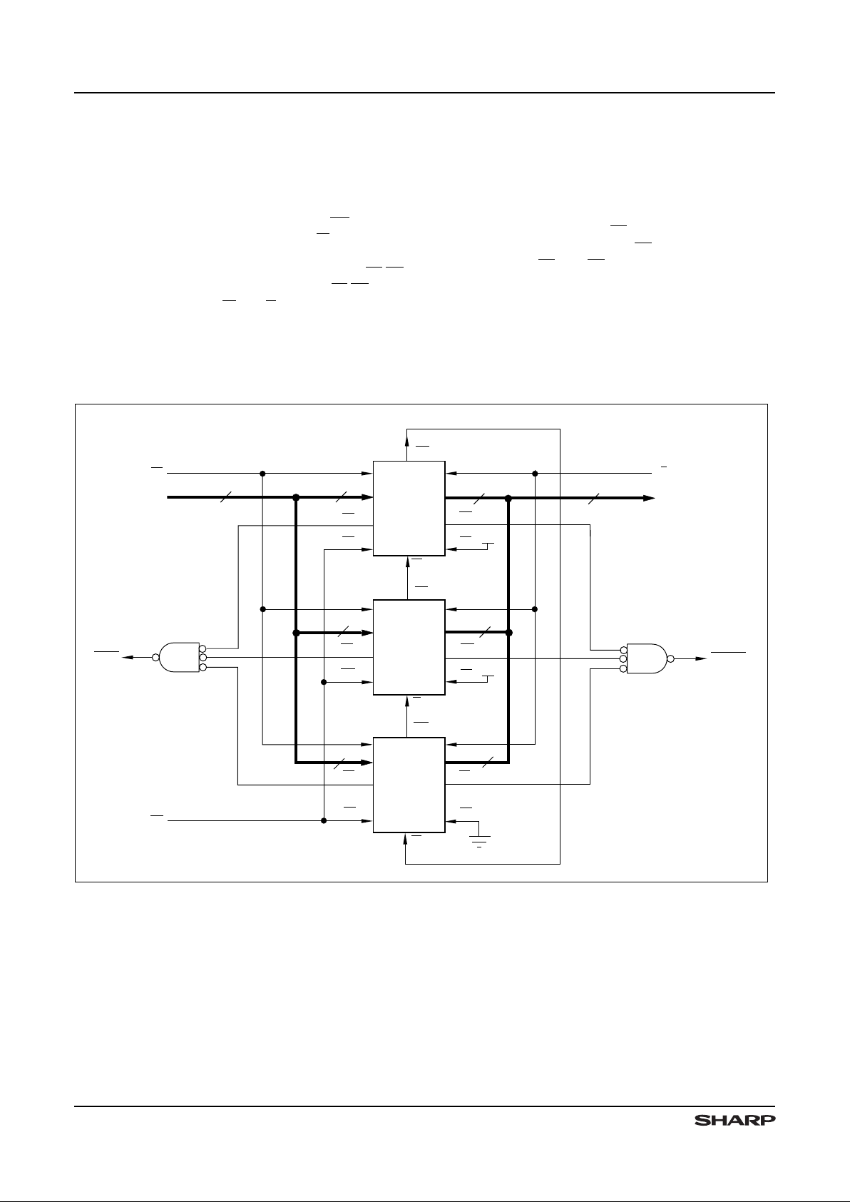
A cascading (depth-expansion) scheme may be implemented by using the Expansion In (XI) input signal and
the Expansion Out (XO/H F) output signal. This allows a
deeper ‘effective FIFO’ to be implemented by using two
or more LH540202 devices, without incurring additional
laten cy (‘fallthro ugh’ or ‘bubblethrough’) d elays, and without the necessity of storing and r et rieving any given dat a
word more than once. In this cascaded operating mode,
one LH540202 device must be designated as the ‘firstload’ or ‘master’ device, by grounding its First-Load
(FL/RT) control input; the remaining LH540202 devices
are designated as ‘slaves,’ by tying their FL/RT inputs
HIGH. Because of the need to share control signals on
pins, the Half-Full Flag and the retransm ission ca pability
are not available for eit her ‘master’ or ‘slave’ LH540202
devices operating in cascaded mode.
FUN CTIONAL DESCRIPTION (con t’d)
DATA OUTPUTS
Q0 - Q
8
FLAG
LOGIC
WRITE
POINTER
READ
POINTER
DATA INPUTS
D0 - D
8
1024 x 9
EF
FF
. . .
540202-1
DUAL-PORT
RAM
ARRAY
INPUT
PORT
CONTROL
R
W
RESET
LOGIC
RS
OUTPUT
PORT
CONTROL
EXPANSION
LOGIC
XO/HF
XI
FL/RT
Figure 3. LH540202 Block Diagr am
LH540202 CMOS 1024 × 9 Asynchronous FIFO
2
Page 3

OPERATIONAL DESCRI PT ION
Reset
The LH540 202 is r eset whenever the Reset input (RS)
is taken LO W. A reset operat io n in itializes bot h the readaddress pointer and the write- add res s point er to point to
location zero, the first physical memory location. During
a reset operation, the state of the XI and FL/RT inputs
determines whethe r the device is in standalone mode or
in depth-cascaded mode. (See Tables 1 and 2.) The
reset operation forces the Empty Flag EF to be asser t e d
(EF = LOW), and t he Half-Full Flag HF and the Full Flag
FF to be de assert ed (HF = FF = HIGH); the Data Out pins
(D0 – D8) are for ced int o a high-im peda nce st ate.
A reset oper at ion is r equired whenever the LH540 202
first is powered up. The Read (R) and Write (W) inputs
may be in any state when the re set oper ation is initiat ed;
but they must be HIGH, before the reset operation is
terminated by a rising edge of RS, by a time t
RRSS
(for
Read) or t
WRSS
(for Write) respectively. (See Figure 10.)
Write
A write cycle is initiated by a falling edge of the Write
(W) contr ol input . Data setup times and hold times must
be observed for the data inputs (D0 – D8). Write operations may occur independently of any ongoing read operation s. However , a write operat ion is possible only if the
FIFO is not full, (i. e., if the Fu ll Flag FF is HIGH).
At the fa lling e dge of W for the first write o peration after
the memory is half filled, the Half-Full Flag is asserted
(HF = LOW). It remains asserted until the difference
between the write pointer and the read pointer indicates
that the data words remaining in the LH540202 are filling
the FIFO memory to less than or equal to one-half of its
total capacity. The Half-Full Flag is deasserted
(HF = HIGH) by the appropriate rising edge of R. (See
Table 3.)
The Full F lag is as serted (FF = LOW) at the falling edge
of W for the write operation which fills the last available
location in th e FIFO memory array. FF = LOW inhibits
further write oper ations until FF is cleared by a va lid r ead
operation. The Full Flag is deasser ted (FF = HIGH) after
the next rising edge of R releases anot he r mem ory lo cation. (See Table 3.)
Read
A read cycle is initiated by a falling edge of the Read
(R) control input. Read data becomes valid at the data
output s (Q0 – Q8) after a time tA from the falling e dge of
R. After R goes HIGH, the data outputs return to a
high-impedance stat e. Read oper ations m ay occur in dependently of any ongoing write operations. However, a
read operation is possible only if the FIFO is not empty
(i.e., if the Empty Flag EF is HIGH).
The LH540202’s in ternal read -ad dress and wri teaddres s point er s oper ate in suc h a way that con secut ive
read operations always access data words in the same
order that they wer e written . The Empty Flag is asse rted
(EF = LOW) after that falling edge of R which accesses
the last available data word in the FIFO memory. EF is
deasserted (EF = HIGH) after the next rising edge of W
loads another valid data word. (See Table 3.)
Data Flow-Through
Read-data flow- throu gh mode occurs when the Read
(R) cont rol inpu t is brought LOW while the FIFO is empty ,
and is held LOW in antic ipation of a write cycle. At the end
of the next write cycle, the Empty F lag EF momentarily is
deasserted, and the data word just written becomes
available at the data outputs (Q0 – Q8) after a maximum time of t
WEF
+ tA. Additional write operations may occur
while the R input remains LOW; but only data from the
first write operation flows through to the data outputs.
Additional data words, if any, may be accessed only by
toggling R.
Write-data flow-through mode occurs when the Write
(W) input is brought LOW while t he FIFO is full, and is
held LOW in anticipation of a read cycle. At the end of the
read cycle, the Full Flag momentarily is deasserted, but
then immediately is reasserted in response to W being
held LOW. A data word is written into the FIFO on the
rising edge of W, which may occur no sooner than
t
RFF
+ t
WPW
after the read oper ation.
PIN DESCRIPT IONS
PIN PIN TYPE
1
DESCRIPTION
D0 – D
8
I
Input Data Bus
Q0 – Q
8 O/Z
Out put Data Bu s
W
I
Write Request
R I Read Request
EF
O
Empt y Flag
FF
O
Full Flag
PIN PIN TYPE
1
DESCRIPTION
XO/HF
O
Expansion Out/Half-Full Flag
XI
I
Expansion In
FL/RT
I
First Load/Retransmit
RS I Res et
V
CC V
Positive Power Supply
V
SS
V
Ground
NOTES:
1. I = Input, O = Output, Z = High-Impedance, V = Power Voltage Level
CMOS 1024 × 9 Asynchronous FIFO LH540202
3
Page 4
OPERATIONAL DESCRIPTION (cont’d)
Retransmit
The FIFO can be made to reread previously-read data
by means of the Retransmit function. A retransmit operation is initiated by pulsing the
RT input LOW. Both R and
W must be deasserted (HIGH) for the duration of the
retransmit pulse. The FIFO’s internal read-address
pointer is reset to point to location zero, the first physical
memory location, while the internal write-address pointer
remains unchanged.
After a retransmit operation, those data words in the
region in between the read-address pointer and the
write-address pointer may be reaccessed by subsequent
read operations. A retransmit operation may affect the
state of the status flags
FF, HF, and EF, depending on
the relocation of the read-address pointer. There is no
restriction on the number of times that a block of data
within an LH540202 may be read out, by repeating the
retransmit operation and the subsequent read operations.
The maximum length of a data block which may be
retransmitted is 1024 words. Note that if the write-address
pointer ever ‘wraps around’ (i.e., passes location zero
more than once) during a sequence of retransmit operations, some data words will be lost.
The Retransmit function is not available when the
LH540202 is operating in depth-cascaded mode,
because the
FL/RT control pin must be used for first-load
selection rather than for retransmission control.
Table 1. Grouping-Mode Determination
During a Reset Operation
XI
FL/
RT
MODE
XO/HF
USAGEXIUSAGE
FL/RT
USAGE
H 1H
Cascaded
Slave
2
XO XI FL
H
1
L
Cascaded
Master
2
XO XI FL
L
X
Standalone
HF (none) RT
NOTES:
1. A rese t operation forces
XO HIGH for the nth FIFO, thus fo rcing XI
HIGH for the (n+1)st FIFO.
2. The terms ‘master’ a nd ‘slave’ refer to operation in depth-c as-
caded groupin g m o de.
3. H = HIGH; L = LOW; X = Don’t Care.
Table 2. Expansion-Pin Usage Acco rding t o
Grouping Mode
I/O PIN
STANDALONE
CASCADED
MASTER
CASCADED
SLAVE
I
XI Grounded
From
XO
(n-1st
FIFO)
From XO
(n-1st
FIFO)
O
XO/HF
Becomes
HF
To
XI
(n+1st
FIFO)
To XI
(n+1st
FIFO)
I
FL/RT
Becomes
RT
Grounded
(Logic
LOW)
Logic
HIGH
Table 3. Status Flags
NUMBER OF UNREAD DATA
WORDS PRESENT WITHIN
1024 × 9 FIFO
FF HF EF
0HHL
1 to 512 H H H
513 to 1023 H L H
1024 L L H
LH540202 CMOS 1024 × 9 Asynchronous FIFO
4
Page 5
OPERATIONAL MO DES
Standalo n e Configuration
When depth cascading is not required for a given
application, the LH540202 is placed in st anda lone mode
by tying the Expansion In input (XI) to ground. This
input is interna lly sampled during a reset operatio n. (See
Table 1.)
Width Expansion
Word-width expansion is implemented by placing
multiple LH540202 devices in parallel. E ach LH540202
should be configured for standalone mode. In this arrangem ent, the behavior of the status flags is ident ical for
all devices; so, in principle, a representative value for
each of these flags could be der ived from any one device .
In practice, it is better to derive ‘composite’ flag values
using external logic, since there may be minor speed
variatio ns between differe nt actual devices. (See Figures
4, 5, a n d 6 .)
WRITE
DATA IN
D
0
- D
8
9
FULL FLAG
RESET
XI
RT
RETRANSMIT
EMPTY FLAG
9
READ
HF
LH540202
W
FF
RS
R
EF
DATA OUT
Q
0
- Q
8
540202-17
Figure 4. Standalone FI FO
(1024 × 9)
DATA IN
D
0
- D
17
18
WRITE
FULL FLAG
RESET
9
READ
EMPTY FLAG
R
EF
XI
RT
R
W
540202-18
RS
RETRANSMIT
RT
XI
HF
W
FF
RS
9
18
DATA OUT
Q
0
- Q
17
9
HF
9
LH540202
LH540202
Figur e 5. FIFO Word- W idth Expansi on
(1024 × 18 )
CMOS 1024 × 9 Asynchronous FIFO LH540202
5
Page 6
OPERATIONAL MO DES (cont’d)
Depth Cascading
Depth cascading is implemented by configuring the
required nu mber of LH540202s in dept h-casca ded mode.
In this arrangem ent, the FIFOs are c onnected in a circular
fashion, with the Expansion Out output (XO) of each
device tied to the Expansion In input (XI) of the next
device. One FIFO in the c ascad e must be designat ed as
the ‘f irst - load’ device, by t ying its First Load input ( FL/RT)
to ground. Al l ot her devices m ust have the ir FL/R T inpu ts
tied HIGH. In this mo de, W and R signals are shared by
all devices, while logic within each LH540202 controls the
steering of data. Only one LH540202 is enabled during
any given write cycle; thus, the common Data In inputs of
all devices are tied together. Likewise, only one
LH540202 is enabled during any given read cycle; thus,
the common Da ta Out outputs of all devices are wireORed toget her
In depth-cascaded mode, external logic should be
used t o gene rate a composite F u ll Flag and a compos ite
Empty Flag, by ANDing the FF ou tputs of all LH540202
devices together and ANDing the EF outputs of all devices
together. Since FF and EF are assertive-LOW signals,
this ‘ANDing’ actually is implemented using an assert iveHIGH physical OR gate. The Half-Full Flag and the
Retr ansm it funct ion are not available in depth- casc aded
mode.
RS
RS
FF
9
9
RS
W
FF
DATA IN
D
0
- D
8
RS
FF
9
9
9
R
9
DATA OUT
Q
0
- Q8
FL
FL
EF
XI
XO
FL
EF
Vcc
Vcc
XO
XO
9
9
XI
540202-19
XI
EMPTY
FULL
EF
LH540202
LH540202
LH540202
Figure 6. FIF O Depth Cas cading
(3072 × 9)
LH540202 CMOS 1024 × 9 Asynchronous FIFO
6
Page 7

OPERATIONAL MO DES (cont’d)
Compound FIFO Expansion
A combination of word-width expansion and depth
cascading may be implemented easily by operating
groups of depth- casc aded FI FOs in parallel.
Bidirect ional FIFO Operat ion
Bidirectional data buff ering between two systems may
be implemente d by operating LH540202 devices in parallel, b ut in o pposite direct ions. The Dat a In in puts of ea ch
LH540202 are tied to the corresp onding Data Out outputs
of another LH540202, which is operating in the opposite
directio n, to form a single b idirectional bus inte rface. Care
must be tak en to assur e that t he app rop riate re ad, write ,
and flag signals are routed to each system. Both wordwidth expansion and depth cascading may be used in
bidirectional applications.
LH540202
DEPTH EXPANSION
BLOCK
LH540202
DEPTH EXPANSION
BLOCK
LH540202
DEPTH EXPANSION
BLOCK
Q
0
- Q
8
DATA OUT
DATA IN
R
W
RS
Q0 - Q
N-1
Q0 - Q
17
540202-20
D
N-9 - DN-1
D18 - D
N-1
D9 - D
N-1
D0 - D
N-1
ARRAY STORES
N-BIT WORDS.
Q
0
- Q
N-10
Figure 7. Compound FIFO Expansion
LH540202
LH540202
SYSTEM A SYSTEM B
Qb
0 - 8
Db
0 - 8
Da
0 - 8
Qa
0 - 8
XI
Wb
Ra
EFa
HFa
RTa
RS
FFb
RTb
HFb
EFb
Rb
540202-21
XI
Wa
FFa
RS
Figure 8. Bidire cti onal FIFO Operat ion
(1024 × 9 × 2)
CMOS 1024 × 9 Asynchronous FIFO LH540202
7
Page 8

ABSOLUTE MAXIMUM RATINGS
1
PARAMETER RATING
Supply Voltage to VSS Potential –0.5 V to 7 V
Signal Pin Voltage to VSS Potential
2
–0.5 V to VCC + 0.5 V (not to exceed 7 V)
DC Output Curr ent
3
±50 mA
Stor age Temp era ture Range –65oC to 150oC
Power Dissip ation (Package Limit ) 1.0 W
DC Volta ge Applied to Outputs In High-Z State –0.5 V to VCC + 0.5 V (not to exceed 7 V)
NOTES:
1. Stresses greater than those listed under ‘A bsolute Maximum Ratings’ may cause permanent damage to the device.
This is a stress rating for transient conditions only. Functional operation of the device at these or any other conditions
outside of those indicated in the ‘Operating Range’ of this specification is not implied. Exposure to absolute maximum
rating conditions for extended period s ma y affect reliability .
2. Negative undershoots of 1.5 V in amplitude are permitted for up to 10 ns once per cycle .
3. Outputs should not be shorted for more than 30 seconds. No more than one output sho uld b e shorted at any time.
OPERATING RANGE
SYMBOL PARAMETER MIN MAX UNIT
T
A
T em peratur e, Ambient
070
°C
VCCSupply Voltage
4.5 5.5 V
V
SS
Supply Voltage
00V
VILLogic LO W Input Vo ltage
1
–0.5 0.8 V
V
IH
Logic HIG H Input V olt age
2.0 VCC + 0.5 V
NOTE:
1. Negative undershoots of 1.5 V in amplitude are permitted for up to 10 ns once per cycle .
DC ELECTRICAL CHARACTERISTICS (Over Operat ing Range)
SYMBOL PARAMETER TEST CONDITIONS MIN MAX UNIT
I
LI
Input Leakage Current VCC = 5.5 V, VIN = 0 V to V
CC
–10 10
µA
I
LO
Outp ut Leakage Cur re nt R ≥ VIH, 0 V ≤ V
OUT
≤ V
CC
–10 10 µA
V
OH
Outp ut HIGH V ol t age IOH = –2.0 mA
2.4 V
V
OL
Outp ut LOW V ol t age IOL = 8.0 mA
0.4 V
I
CC
Ave rage Supply Current
1
Measur ed at f = 40 MHz
100 mA
I
CC2
Average Standby Current
1
All Input s = V
IH
15 mA
I
CC3
Power Down Curr ent
1
All Input s = VCC – 0. 2 V
5mA
NOTE:
1. I
CC
, I
CC2
, and I
CC3
are dependent upon actual output loading and cycl e r a tes. Specified values are with outputs open.
LH540202 CMOS 1024 × 9 Asynchronous FIFO
8
Page 9

AC TEST CONDITIONS
PARAMETER RATING
Input Pulse Levels
VSS to 3 V
Input Rise and Fall T imes (10% t o 90% ) 5 ns
Input Timing Reference Levels
1.5 V
Output Re ferenc e Levels
1.5 V
Output Load , Timin g T es ts
Figure 9
CAP ACITANCE
1,2
PARAMET ER RA TING
CIN (Input Capacitance)
5 pF
C
OUT
(Output Capacitanc e)
7 pF
NOTES:
1. Sample tested only.
2. Capacitances are maximum values at 25
o
C, measured at 1.0 MHz,
with VIN = 0 V.
540202-4
DEVICE
UNDER
TEST
+5 V
30 pF
1.1 k Ω
680 Ω
INCLUDES JIG AND SCOPE CAPACITANCES
*
*
Figu r e 9. Out put Lo a d Circ uit
CMOS 1024 × 9 Asynchronous FIFO LH540202
9
Page 10

AC ELECTRICAL CHARACTERISTICS 1 (Over Operat ing Range)
SYMBOL PARAMETER
tA = 15 ns tA = 20 ns tA = 25 ns tA = 35 ns tA = 50 ns
UNIT
MIN MAX MIN MAX MIN MAX MIN MAX MIN MAX
READ CYCLE TIMING
t
RC
Read Cycl e T ime 25 – 30 – 35 – 45 – 65 – ns
t
A
Access Time – 15 – 20 – 25 – 35 – 50 ns
t
RR
Read Rec over y Ti me 10 – 10 – 10 – 10 – 15 – ns
t
RPW
Read Puls e Width
2
15–20–25–35–50–ns
t
RLZ
Data Bus Active from Read LOW
3
5–5–5–5–5–ns
t
WLZ
Data Bus Active from Write HIGH
3,4
10–10–10–10–10–ns
t
DV
Data Valid from Read Pulse HIGH 5 – 5–5–5–5–ns
t
RHZ
Data Bus High -Z fro m Read HIGH
3
–15–15–15–15–20ns
WRITE CYCLE TIMING
t
WC
Wri te Cycl e Ti me 25 – 30 – 35 – 45 – 65 – ns
t
WPW
Write Pulse Width
2
15–20–25–35–50–ns
t
WR
Wri te Reco very Tim e 10 – 10 – 10 – 10 – 15 – ns
t
DS
Data Set up T ime 10 – 10 – 10 – 15 – 20 – ns
t
DH
Data Hol d Ti me 0 – 0–0–0–0–ns
RESET TIMING
t
RSC
Reset Cycle Time 25 – 30 – 35 – 45 – 65 – ns
t
RS
Reset Pulse Width
2
15–20–25–35–50–ns
t
RSR
Reset Recovery Time 10 – 10 – 10 – 10 – 15 – ns
t
RRSS
Read HIG H to RS HIGH 15–20–25–35– 50–ns
t
WRSS
Write HIGH to RS HIGH 15 – 20 – 25 – 35 – 50 – ns
RETRANSMIT TIMING
5
t
RTC
Retra nsm it Cycl e Ti me 25 – 30 – 35 – 45 – 65 – ns
t
RT
Retransmit Pulse Width
2
15–20–25–35–50–ns
t
RTR
Retra nsm it Reco very Tim e 10 – 10 – 10 – 10 – 15 – ns
FLAG TIMING
t
EFL
Reset LOW to Empty Flag LOW – 25 – 30 – 35 – 45 – 65 ns
t
HFH,FFH
Reset LOW to Half-Full and Full
Flags HIGH
–25–30–35–45–65ns
t
REF
Read LOW to Empt y Flag LOW – 15 – 20 – 25 – 35 – 45 ns
t
RFF
Read HIGH to Full Flag HIGH – 15 – 20 – 25 – 35 – 45 ns
t
WEF
Write HIGH to Empty Flag HIGH – 15 – 20 – 25 – 35 – 45 ns
t
WFF
Write LOW to Full Flag LOW – 15 – 20 – 25 – 35 – 45 ns
t
WHF
Write LOW to Half-Full Flag LOW – 15 – 20 – 25 – 35 – 45 ns
t
RHF
Read HIGH to Half-Full Flag HIGH
–15–20–25–35–45ns
EXPANSION TIMING
t
XOL
Expansion Out LOW
–18–20–25–35–50ns
t
XOH
Expansion Out HIGH – 18 – 20 – 25 – 35 – 50 ns
t
XI
Expansion In Pulse Width 15 – 20 – 25 – 35 – 50 – ns
t
XIR
Expansion In Recovery Time 10 – 10 – 10 – 10 – 10 – ns
t
XIS
Expan sion in Setup T ime
7 –10–10–15–15–ns
NOTES:
1. All timing measurements are performed at ‘AC Test Condition’ levels.
2. Pulse widths less than minimum value are not allowed.
LH540202 CMOS 1024 × 9 Asynchronous FIFO
10
Page 11

TIMING DIAGRAMS
t
RS
EFL
t
RSR
t
RRSS
t
WRSS
t
FFHtHFH
t
,
RS
R,W
EF
FF,HF
540202-14
t
RSC
NOTES:
1. t
RSC
= tRS + t
RSR
.
2. W and R ≥ VIH around the rising edge of RS.
3. The Data Out pins (D
0
- D8) are forced into a
high-impedance state whenever EF = LOW.
Figure 10. Reset Timing
W
t
WPW
t
RLZ
t
A
t
WC
t
A
t
RPW
t
DV
t
RHZ
VALID DATA OUT
t
RR
R
t
RC
t
WR
t
DH
t
DS
540202-5
Q0 - Q
8
D0 - D
8
VALID DATA OUT
VALID DATA INVALID DATA IN
Figure 1 1 . Asynchronous Write and Read Operat ion
CMOS 1024 × 9 Asynchronous FIFO LH540202
11
Page 12

TIMING DIAGRAMS (co nt ’d)
FF
R
t
RFF
t
WFF
LAST WRITE FIRST READ
W
540202-6
Figure 12. Full Fl ag From Last Writ e to Firs t Read
EF
W
R
t
WEF
t
REF
LAST READ FIRST WRITE
540202-7
NOTE: The Data Out pins (D0 - D8) are forced into a
high-impedance state whenever EF = LOW.
Figure 13. Empty Flag From Last Read to First Writ e
LH540202 CMOS 1024 × 9 Asynchronous FIFO
12
Page 13

TIMING DIAGRAMS (co nt ’d)
RPE
t
WEF
t
REF
t
WLZ
t
A
t
540202-8
W
R
EF
D0 - D
8
Q0 - Q
8
VALID DATA OUT
VALID DATA IN
NOTES:
1. t
RPE
= t
RPW
2. t
RPE
: Effective Read Pulse Width after Empty Flag HIGH.
3. The Data Out pins (D
0
- D8) are forced into a
high-impedance state whenever EF = LOW.
Figure 14. Read Data Fl ow -Thr ough
WPF
t
R
W
FF
t
WFF
t
RFF
t
DH
t
DS
t
A
D0 - D
8
Q0 - Q
8
NOTES:
1. t
WPF
= t
WPW
2. t
WPF
: Effective Write Pulse Width after Full Flag HIGH.
540202-9
VALID DATA OUT
VALID DATA IN
Figure 15. Write Data Flow-Thr ough
CMOS 1024 × 9 Asynchronous FIFO LH540202
13
Page 14

TIMING DIAGRAMS (co nt ’d)
t
WEF
W
t
RPE
EF
R
540202-10
NOTES:
1. t
RPE
= t
RPW
2. t
RPE
: Effective Read Pulse Width after Empty Flag HIGH.
3. The Data Out pins (D
0
- D8) are forced into a
high-impedance state whenever EF = LOW.
Figure 16. Empty Flag Timin g
R
FF
W
540202-11
NOTES:
1. t
WPF
= t
WPW
2. t
WPF
: Effective Write Pulse Width after Full Flag HIGH.
t
RFF
t
WPF
Figure 17 . Full Flag Ti min g
LH540202 CMOS 1024 × 9 Asynchronous FIFO
14
Page 15

TIMING DIAGRAMS (co nt ’d)
HF
W
R
t
RHF
t
WHF
540202-12
HALF-FULL
OR LESS
MORE THAN
HALF-FULL
HALF-FULL
OR LESS
Figure 18. Hal f -Full Flag Timi n g
540202-13
NOTES:
1. t
RTC
= t
RT
+ t
RTR
2. FF, HF and EF may change state during retransmit, but they will become valid by t
RTC
.
RT
t
RTR
t
RT
R,W
Figure 19. Retransmit Timin g
CMOS 1024 × 9 Asynchronous FIFO LH540202
15
Page 16

TIMING DIAGRAMS (co nt ’d)
t
XOL
t
XOH
READ FROM
LAST VALID
LOCATION
t
XOH
t
XOL
XO
540202-15
WRITE TO LAST
AVAILABLE
LOCATION
W
R
Figure 20. Expa nsion-Out Timi n g
t
XIS
R
540202-16
XI
W
WRITE TO FIRST
AVAILABLE
LOCATION
t
XIS
READ FROM FIRST
VALID
LOCATION
t
XIR
t
XI
Figure 21. Expansion-In Timing
LH540202 CMOS 1024 × 9 Asynchronous FIFO
16
Page 17

PACKAGE DIAGRAMS
28DIP-3
7.49 [0.295]
7.11 [0.280]
0.51 [0.020] MIN
4.57 [0.180]
MAX
3.43 [0.135]
3.18 [0.125]
2.54 [0.100]
TYP.
0.53 [0.021]
0.38 [0.015]
0.30 [0.012]
0.20 [0.008]
DETAIL
DIMENSIONS IN MM [INCHES]
34.80 [1.370]
34.54 [1.360]
0° TO 15°
MAXIMUM LIMIT
MINIMUM LIMIT
3.30 [0.130]
7.62 [0.300]
TYP.
28DIP (DIP28-W-300)
28-pin, 300-mil PDIP
28SOJ300
DIMENSIONS IN MM [INCHES]
MAXIMUM LIMIT
MINIMUM LIMIT
28SOJ (SOJ28-P-300)
1.27 [0.050]
TYP.
0.53 [0.021]
0.33 [0.013]
DETAIL
7.9 [0.311]
7.5 [0.295]
8.63 [0.340]
8.23 [0.324]
18.7 [0.736]
18.3 [0.720]
1.15 [0.045]
0.85 [0.033]
0.64 [0.025] MIN
7.0 [0.276]
6.6 [0.260]
2.6 [0.102]
2.2 [0.087]
3.7 [0.146]
3.3 [0.130]
0.20 [0.008]
0.8 [0.031]
0.6 [0.024]
0.102 [0.004]
114
28 15
28-pin, 300-mil SOJ
CMOS 1024 × 9 Asynchronous FIFO LH540202
17
Page 18

ORDERING INFO RMATION
1.27 [0.050]
4 SIDES BSC
14.05 [0.553]
13.89 [0.547]
15.11 [0.595]
14.86 [0.585]
11.51 [0.453]
11.35 [0.447]
12.57 [0.495]
12.32 [0.485]
3.56 [0.140]
3.12 [0.123]
2.41 [0.095]
1.52 [0.060]
0.81 [0.032]
0.66 [0.026]
0.53 [0.021]
0.33 [0.013]
32PLCC
MAXIMUM LIMIT
MINIMUM LIMIT
DIMENSIONS IN MM (INCHES)
0.38 [0.015]
MIN
DETAIL
10.92 [0.430]
9.91 [0.390]
13.46 [0.530]
12.45 [0.490]
0.10 [0.004]
32PLCC (PLCC32-P-R450)
32-pi n, 450-mil PLCC
D 28-pin, 300-mil Plastic DIP (DIP28-W-300)
K 28-pin, 300-mil SOJ * (SOJ28-P-300)
U 32-pin Plastic Leaded Chip Carrier (PLCC32-P-R450)
LH540202
Device Type
X
Package
- ##
Speed
540202MD
CMOS 1024 x 9 FIFO
Example: LH540202U-25 (CMOS 1024 x 9 FIFO, 32-pin PLCC, 25 ns)
15
20
25
35
50
Access Time (ns)
* Contact a Sharp representative for availability of SOJ package.
LH540202 CMOS 1024 × 9 Asynchronous FIFO
18
 Loading...