

Datasheet LH52256CT-70LL, LH52256CN-70LL, LH52256CH-70LL, LH52256CD-70LL, LH52256CHT-70LL Datasheet (Sharp)
...Page 1
LH52256C/CH
CMOS 256K (32K × 8) Sta tic RA M
FEATURES
•• 32,768 × 8 bi t organ ization
•• Access time: 70 ns (MAX.)
•• Supply curre nt :
Operating : 45 mA (MAX.)
10 mA (MAX.) (t
RC
, tWC = 1 µs)
Standb y: 40 µA (MAX.)
•• Data retention current: 1.0 µA (MAX.)
(V
CCDR
= 3 V, TA = 25°C)
•• Wide o pera tin g vol ta ge ran g e:
4.5 V ± 5.5 V
•• Operatin g temperatu re:
Commeri cal tempe rature 0°C t o +70°C
Industrial temperature -40° to +85°C
•• Fully-static operatio n
•• Three-state outputs
•• Not design ed or rated as rad iation
hardene d
•• Packa ge:
28-pi n , 600 -mil DIP
28-pi n , 450 -mil S OP
28-pi n , 300 -mil SK-DIP
28-pi n , 8 × 3 mm
2
TSOP (Type I)
•• N-type bulk silicon
DESCRIPTION
The LH52256C is a Static RAM organized as
32,768 × 8 bits which provides low-power standby
mode. It is fabricated using silicon-gate CMOS process
technology.
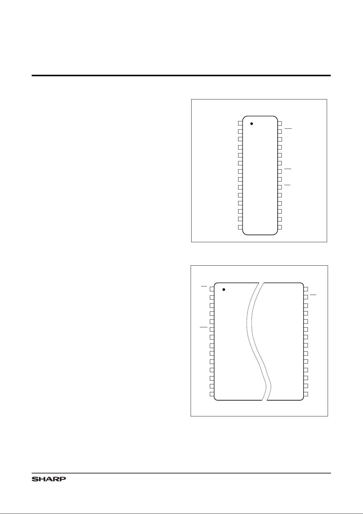
PIN CONNECTIONS
52256C-1
1
2
3
4
5
6
7
8
9
10
11
12
13
14
A
14
A
12
A
7
A
6
A
5
A
4
A
3
A
2
A
1
A
0
28
27
26
25
24
23
22
21
20
19
18
17
16
15
V
CC
WE
A
9
A
11
OE
A
10
I/O
6
I/O
5
GND
I/O
8
I/O
7
CE
A
13
A
8
I/O
1
I/O
2
I/O
3
I/O
4
28-PIN DIP
28-PIN SK-DIP
28-PIN SOP
TOP VIEW
Figure 1. Pin Connections
2
3
4
5
6
9
10
7
8
A
11
11
1
28
27
26
25
22
21
24
23
20
19
A
10
28-PIN TSOP (Type I)
12
13
14
17
16
18
15
OE
A
8
A
9
A
13
WE
A
12
A
14
I/O
3
I/O
2
A
1
I/O
8
CE
I/O
6
I/O
7
GND
I/O
5
I/O
4
I/O
1
A
0
52256C-8
V
CC
A
7
A
6
A
5
A
4
A
3
A
2
NOTE: Reverse bend available on request.
Figu re 2. TSOP (Type I) Pin Connections
1
Page 2
A
4
A
3
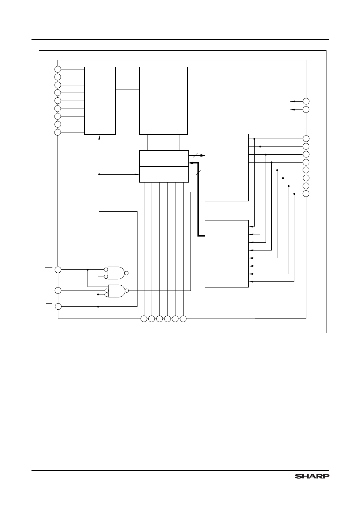
52256C-2
MEMORY
ARRAY
(512 x 512)
A
5
ROW
DECORDER
WE
A
6
A
7
27
A
12
V
CC
GND
OE
22
28
14
A
13
CE
20
COLUMN I/O
CIRCUIT
COLUMN
DECODER
OUTPUT
BUFFERS
I/O
1
11
12
13
15
16
17
18
19
I/O
2
I/O
3
I/O
4
I/O
5
I/O
6
I/O
7
I/O
8
10 9
8
212423
INPUT
DATA
CONTROL
26
2
3
4
5
6
7
A
0A1A2A10A9A11
A
14
A
8
25
1
8
8
Figure 3. LH52256C Block Diagram
PIN DESCRIPTI ON
SIGNA L PIN N AME
A0 - A
14
Addre ss inputs
CE
Chip ena ble
WE
Write e nab le
OE Outpu t e nab le
SIGNAL PIN NAM E
I/O1 - I/O
8
Data i npu ts and ou tpu ts
V
CC
Power sup ply
GND
Ground
LH52256C /CH CMOS 256K (32K × 8) Static RAM
2
Page 3
TRUTH TABLE
CE WE OE MODE I/O1 - I/O
8
SUPPLY CURRENT NOTE
H X X Standby High impedance Standby (ISB)1
L H L Read Data output Active (I
CC
)1
L H H Output disable High impedance Active (I
CC
)1
L L X Write Data input Active (I
CC
)1
NOTE:
1. X = Don’t care, L = Low, H = High
ABSOLUTE MAXIMUM RATINGS
PARAMETER SYMBOL RATING UNIT NOTE
Suppl y v olt age V
CC
–0.5 to +7.0 V 1
Input vol tage V
IN
–0.5 to VCC + 0.5 V 1, 2
Operat ing te mpe ratu re T
OPR
0 to +70
°C
Storag e t emp era ture T
STG
–65 to +150
°C
NOTES:
1. The maximum applicable voltage on any pin with respect to GND.
2. Undershoot of -3.0 V is al lowed width of pulse below 50 ns.
RECOMMENDED DC OPERATING CONDITIONS (TA = 0°C to +70°C)
PARAM ETER SYMBOL MIN. TYP. MAX. UNIT NOTE
Suppl y v olt age V
CC
4.5 5.0 5.5 V
Input vol tage
V
IH
2.2
VCC + 0.5 V
V
IL
–0.5
0.8 V 1
NOTE:
1. Undershoot of -3.0 V is al lowed width of pulse below 50 ns.
CMOS 256K (32K × 8) Static RAM LH 52256C/CH
3
Page 4

DC ELECTRICAL CHARACTERISTICS (TA = 0°C to +70°C, VCC = 4.5 V to 5.5 V)
PARAMETER SYMBOL CONDITIONS MIN. TYP . MAX. UNIT
Input lea kage
curren t
I
LI
VIN = 0 V to V
CC
–1.0
1.0 µA
Output le aka ge
curren t
I
LO
CE = VIH or OE = V
IH
V
I/O
= 0 V to V
CC
–1.0
1.0
µA
Operat ing su ppl y
curren t
I
CC
Minimum cycle, VIN = VIL or V
IH
I
I/O
= 0 mA, CE = V
IL
25 45.0
mA
I
CC1
tRC, tWC = 1 µs, VIN = VIL or VIH,
I
I/O
= 0 mA, CE = V
IL
10.0
Standb y c urr ent
I
SB
CE ≥ VCC – 0.2 V
0.6 40.0
µA
I
SB1
CE = V
IH
3.0 mA
Output vo lta ge
V
OL
IOL = 2.1 mA
0.4
V
V
OH
IOH = -1.0 mA 2.4
NOTE:
Typical values at V
CC
= 5.0 V, TA = 2 5 °C
AC ELECTRICAL CHARACTERISTICS
AC Test Conditions
PARAMETE R MODE NOTE
Input pul se level
0.6 V to 2.4 V
Input ris e a nd f all ti me
10 ns
Input and ou tpu t ti min g R ef. le vel 1.5 V
Output lo ad
1 TTL + C
L
(100 pF) 1
NOTE:
1. In cluding scope and jig capacitance.
READ CYCLE (TA = 0°C to +70°C, VCC = 4.5 V to 5.5 V)
PARAMETER SYMBOL MIN. MAX. UNIT NOTE
Read c yc le t ime t
RC
70
ns
Addres s a cc ess ti me t
AA
70 ns
CE acc es s t ime t
ACE
70 ns
Output en abl e t o ou tpu t v ali d
t
OE
35 ns
Output ho ld from ad dre ss cha nge t
OH
10
ns
CE Low to ou tpu t a cti ve t
LZ
10
ns 1
OE Low to ou tpu t ac tiv e t
OLZ
5
ns 1
CE Hig h t o o utp ut i n H igh im ped anc e t
HZ
030ns1
OE Hig h t o o utp ut i n H igh im ped anc e t
OHZ
030ns1
NOTES:
1.
Active output to high-impedance and high-impedance t o output active tests specified for a ±200 mV
transition from steady state levels int o the test load.
LH52256C /CH CMOS 256K (32K × 8) Static RAM
4
Page 5

WRITE CYCLE (TA = 0°C to +70°C, VCC = 4.5 V to 5.5 V)
PARAMETER SYMBOL MIN. MAX. UNIT NOTE
Write c ycl e t ime t
WC
70
ns
CE Low to en d o f wr ite t
CW
45
ns
Addres s v al id t o e nd of writ e
t
AW
45
ns
Addres s s etu p t ime t
AS
0
ns
Write p uls e w idt h t
WP
35
ns
Write re co ver y ti me t
WR
0
ns
Input dat a s etu p ti me
t
DW
30
ns
Input dat a h old tim e t
DH
0
ns
WE Hig h t o o utp ut a cti ve t
OW
5
ns 1
WE Low to ou tpu t in Hi gh
impeda nce
t
WZ
030ns1
OE Hig h t o o utp ut i n H igh
impeda nce
t
OHZ
030ns1
NOTE:
1.
Active output to high-impedance and high-impedance t o output active tests specified for a ±200 mV
transition from steady state levels int o the test load.
CAPACITANCE (TA = 25°C, f = 1MHz)
PARAMETER SYMBOL CONDITIONS MIN. TYP. MAX. UNIT NOTE
Input cap acitan ce C
IN
VIN = 0 V
7pF1
I/O ca pac ita nce
C
I/O
V
I/O
= 0 V
10 pF 1
NOTE:
1. Th is parameter is sampled and not production tested.
DATA RETENTION CHARACTERISTICS (TA = 0°C to +70°C)
PARAMETER S YMBOL CONDITIONS MIN. TYP. MAX. UNIT NOTE
Data r ete nti on s up ply vo lta ge
V
CCDR
CE ≥ V
CCDR
– 0.2 V 2.0
5.5 V
Data r ete nti on s up ply cu rren t I
CCDR
V
CCDR
= 3.0 V
CE ≥ V
CCDR
– 0.2 V
T
A
= 25°C
0.3 1.0
µA
TA = 40°C
3.0
15
Chip enab le setup tim e t
CDR
0
ns
Chip e nab le hol d t ime t
R
t
RC
ns 1
NOTE:
1. tRC = Read cycle time.
2.
Typical values at TA = 25° C
CMOS 256K (32K × 8) Static RAM LH 52256C/CH
5
Page 6

D
OUT
DATA VALID
t
RC
t
AA
t
ACE
t
LZ
t
OLZ
t
OH
t
OHZ
t
HZ
52256C-3
ADDRESS
t
OE
OE
CE
NOTE: WE is HIGH for Read Cycle.
Figure 4. Read Cycle
LH52256C/CH CMOS 256K (32K × 8) Static RAM
6
Page 7

D
IN
52256C-4
ADDRESS
OE
t
WC
t
AW
t
WR
t
CW
t
AS
t
WP
t
OHZ
t
DW
t
WR
t
DH
DATA VALID
CE
WE
D
OUT
1. A write occurs during the overlap of a LOW CE, and a LOW WE.
A write begins at the latest transition among CE going LOW, and
WE going LOW. A write ends at the earliest transition among CE
going HIGH, and WE going HIGH. t
WP
is measured from the beginning
of write to the end of write.
2. t
CW
is measured from the later of CE going LOW to the end of write.
3. t
AS
is measured from the address valid to the beginning of write.
4. t
WR
is measured from the end of write to the address change.
5. During this period, I/O pins are in the output state, therefore the input
signals of opposite phase to the outputs must not be applied.
6. If CE goes LOW simultaneously with WE going LOW or after WE going
LOW, the outputs remain in high impedance state.
7. If CE goes HIGH simulaneously with WE going HIGH or before WE
going HIGH, the outputs remain in high impedance state.
NOTES:
(NOTE 4)
(NOTE 2)
(NOTE 1)
(NOTE 3)
(NOTE 6)
(NOTE 5)
(NOTE 4)
Figure 5. Write Cycl e (O E Controlled)
CMOS 256K (32K × 8) Static RAM LH 52256C/CH
7
Page 8

DATA VALID
t
DH
t
DW
WE
D
IN
t
CW
ADDRESS
t
WC
52256C-5
t
WR
t
AW
CE
t
AS
t
WZ
t
WP
(NOTE 2
)
(NOTE 4)
(NOTE 3)
D
OUT
(NOTE 6)
(NOTE 1)
t
WR
t
OW
(NOTE 7)
(NOTE 5)
(NOTE 4)
1. A write occurs during the overlap of a LOW CE, and a LOW WE.
A write begins at the latest transition among CE going LOW, and
WE going LOW. A write ends at the earliest transition among CE
going HIGH, and WE going HIGH. t
WP
is measured from the beginning
of write to the end of write.
2. t
CW
is measured from the later of CE going LOW to the end of write.
3. t
AS
is measured from the address valid to the beginning of write.
4. t
WR
is measured from the end of write to the address change.
5. During this period, I/O pins are in the output state, therefore the input
signals of opposite phase to the outputs must not be applied.
6. If CE goes LOW simultaneously with WE going LOW or after WE going
LOW, the outputs remain in high impedance state.
7. If CE goes HIGH simulaneously with WE going HIGH or before WE
going HIGH, the outputs remain in high impedance state.
NOTES:
Figure 6. Write Cycle (OE Low Fixed)
t
CDR
V
CC
4.5 V
2.2 V
V
CCDR
0 V
CE
CE ≥ V
CCDR
- 0.2 V
DATA RETENTION MODE
t
R
52256C-6
CE CONTROL
Data Retention Timing Chart
CE Control led
LH52256C/CH CMOS 256K (32K × 8) Static RAM
8
Page 9

PACKAGE DIAGRAMS
DIMENSIONS IN MM [INCHES]
MAXIMUM LIMIT
MINIMUM LIMIT
28DIP (DIP028-P-0600)
114
1528
28DIP-2
13.45 [0.530]
12.95 [0.510]
0.51 [0.020] MIN.
5.20 [0.205]
5.00 [0.197]
3.50 [0.138]
3.00 [0.118]
2.54 [0.100]
TYP.
0.60 [0.024]
0.40 [0.016]
0.30 [0.012]
0.20 [0.008]
DETAIL
36.30 [1.429]
35.70 [1.406]
0° TO 15°
4.50 [0.177]
4.00 [0.157]
15.24 [0.600]
TYP.
DIMENSIONS IN MM [INCHES]
MAXIMUM LIMIT
MINIMUM LIMIT
28SOP (SOP028-P-0450)
12.40 [0.488]
11.60 [0.457]
8.80 [0.346]
8.40 [0.331]
10.60 [0.417]
18.20 [0.717]
17.80 [0.701]
0.15 [0.006]
1.025 [0.040]
0.20 [0.008]
0.00 [0.000]
1.025 [0.040]
2.40 [0.094]
2.00 [0.079]
0.20 [0.008]
0.10 [0.004]
0.50 [0.020]
0.30 [0.012]
1.27 [0.050]
TYP.
28 15
141
1.70 [0.067]
1.70 [0.067]
28SOP
CMOS 256K (32K × 8) Static RAM LH 52256C/CH
9
Page 10

0.51 [0.020] MIN
4.60 [0.181]
4.20 [0.205]
3.50 [0.138]
3.00 [0.118]
1.78 [0.070]
TYP.
0.56 [0.022]
0.36 [0.014]
0.30 [0.012]
0.20 [0.008]
DETAIL
25.75 [1.014]
25.25 [0.994]
0° TO 15°
4.05 [0.159]
3.65 [0.144]
28SDIP (SDIP28-P-400)
DIMENSIONS IN MM [INCHES]
MAXIMUM LIMIT
MINIMUM LIMIT
8.80 [0.346]
8.40 [0.331]
14
15
1
28
10.16 [0.400]
TYP.
28SDIP
DIMENSIONS IN MM [INCHES]
MAXIMUM LIMIT
MINIMUM LIMIT
28TSOP (TSOP028-P-0813)
28
1
28TSOP
14
15
0.28 [0.011]
0.12 [0.005]
0.55 [0.022]
TYP.
12.00 [0.472]
11.60 [0.457]
13.70 [0.539]
13.10 [0.516]
8.20 [0.323]
7.80 [0.307]
0.15 [0.006]
1.10 [0.043]
0.90 [0.035]
1.20 [0.047]
MAX.
12.60 [0.496]
12.20 [0.480]
0.20 [0.008]
0.10 [0.004]
0.20 [0.008]
0.00 [0.000]
1.10 [0.043]
0.90 [0.035]
0.425 [0.017]
0.20 [0.008]
0.00 [0.000]
0 - 10°
DETAIL
0.425 [0.017]
LH52256C/CH CMOS 256K (32K × 8) Static RAM
10
Page 11

Low-Low-power standby
LH52256C
Device Type
X
Package
- ##
Speed
52256C-7
CMOS 32K x 8 Static RAM
Example: LH52256C-70LL (CMOS 32K x 8 Static RAM, Low-Low-power standby, 70 ns, 28-pin, 600-mil DIP)
70 Access Time (ns)
LL
Power
Blank 28-pin, 600-mil DIP (DIP028-P-0600)
D 28-pin, 300-mil SK-DIP (DIP028-P-0300)
N 28-pin, 450-mil SOP (SOP028-P-0450)
T 28-pin, 8 x 13 mm
2
TSOP (Type I) (TSOP028-P-0813)
X
Operating
Temp
Blank 0° to +70°C
H -4° to +85°C
ORDERING INFORMATION
CMOS 256K (32K × 8) Static RAM LH 52256C/CH
11
 Loading...