

Page 1
LH521028A
CMOS 64K × 18 Static RAM
FEATURES
•• Fast A ccess T imes: 15/17/ 20/25/ 35 ns
•• Wide Word (18-Bits) for:
– Improved Performance
– Reduced Component Count
– Nine-bit Byte for Parit y
•• T ransparent Address Latch
•• Reduced Loading on Address Bus
•• Low-Power Stand-by Mode when
Deselected
•• TTL Compatible I/O
•• 5 V
± 10% Supply
•• 2 V Data Retention
•• JEDEC Standard Pinout
•• Package: 52-Pin PLCC
FUNCTIONAL DESCRIPTION
The LH521028 is a high-speed 1,179,648-bit CMOS
SRAM organized as 64K × 18. A fast, efficient design is
obtained with a CMOS periphery and a matrix constructed with polysilicon load memory cells. The
LH521028 is available in a compact 52- Pin PLCC, which
along with the six pairs of supply terminals, provide for
reliable operation.
The control signals include Write Enable (W), Chip
Enable (E), High an d Low By te Select ( SL and SH), Out put
Enable (G) and Address Latch Enable (ALE). The wide
word provides for reduced component count, improved
density, r educed Addr ess bus loading and improved performance . The wide word also allows for byte-parit y with
no additional RAM required .
This RAM is fully static in opera tion. The Chip Enable
(E) control permits Read and Write operations when
active (LOW) or places the RAM in a low-power standby
mode wh en inactive (HI GH).The Byt e-select controls, S
H
and SL, are also used to enable or disable Read and Write
operations on the high and the low bytes. The Address
Latches are transpar ent wh en ALE is HIGH (for a pplications not requiring a latch), and are latch ed when ALE is
LOW. The Address Latches and the wi de word help to
eliminate the need for external Address bus buffers and/or
latches .
Write cycles occur when Chip Enable (E), SH and/or
SL, and Write Enable (W) are LOW. The Byte-select
signals can be used for Byt e-write oper ations by disabling
the other byte during the Write operation. Data is transferred from the DQ pins to the memor y location specified
by the 16 address lines. The proper use of the Output
Enable control (G) can pre vent bus con ten tion.
When E and either SH or SL are LO W and W is HIGH,
a static Read will occur at the mem or y location spec ifie d
by the addr ess line s. G must be brought LOW to enable
the outputs. Since the device is fully static in operation,
new Read cycles can be performed by simply changing
the address with ALE HIGH.
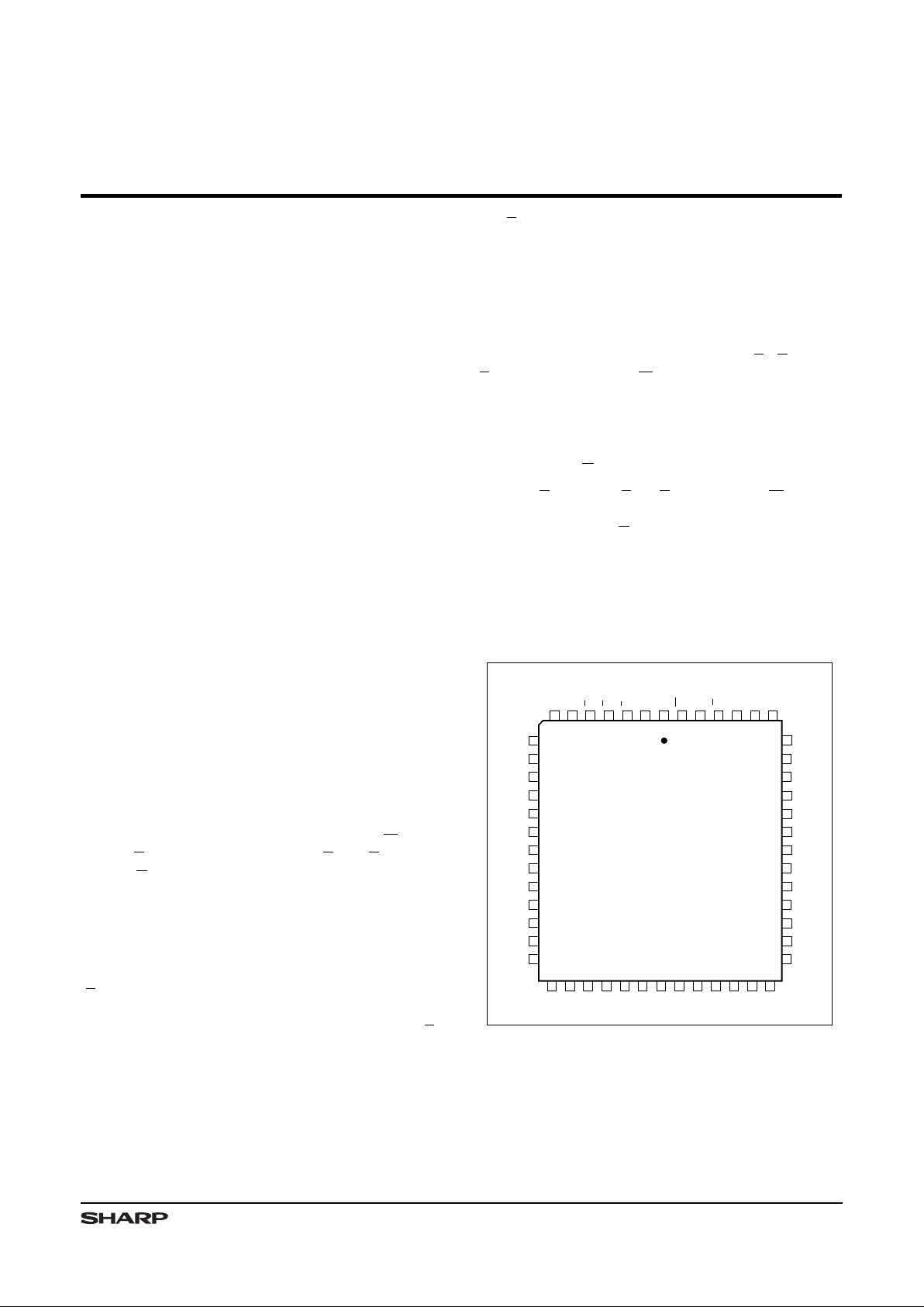
PIN CONNECTIONS
521028-1D
8
9
10
11
12
13
14
15
16
17
18
19
20
46
45
44
43
42
41
40
39
38
37
36
35
34
7 6 5 4 3 2 1 525150494847
21 22 23 24 25 26 27 28 29 30 31 32 33
DQ
8
DQ
7
DQ
6
V
CC
V
SS
DQ
5
DQ
4
DQ
3
DQ
2
V
SS
V
CC
DQ
1
DQ
0
DQ
9
DQ
10
V
CC
V
SS
DQ
11
DQ
12
DQ
13
DQ
14
V
SS
V
CC
DQ
15
DQ
16
DQ
17
A
1
A
0
E
S
H
S
L
V
CC
V
SS
W
ALE
G
A
15
A
14
A
13
A
3
A
5
A
6
A
7
V
SS
V
CC
A
8
A
10
A
11
A
12
A
4
A
9
A
2
52-PIN PLCC
TOP VIEW
Figure 1. Pin Connecti ons for PLCC Package
1
Page 2
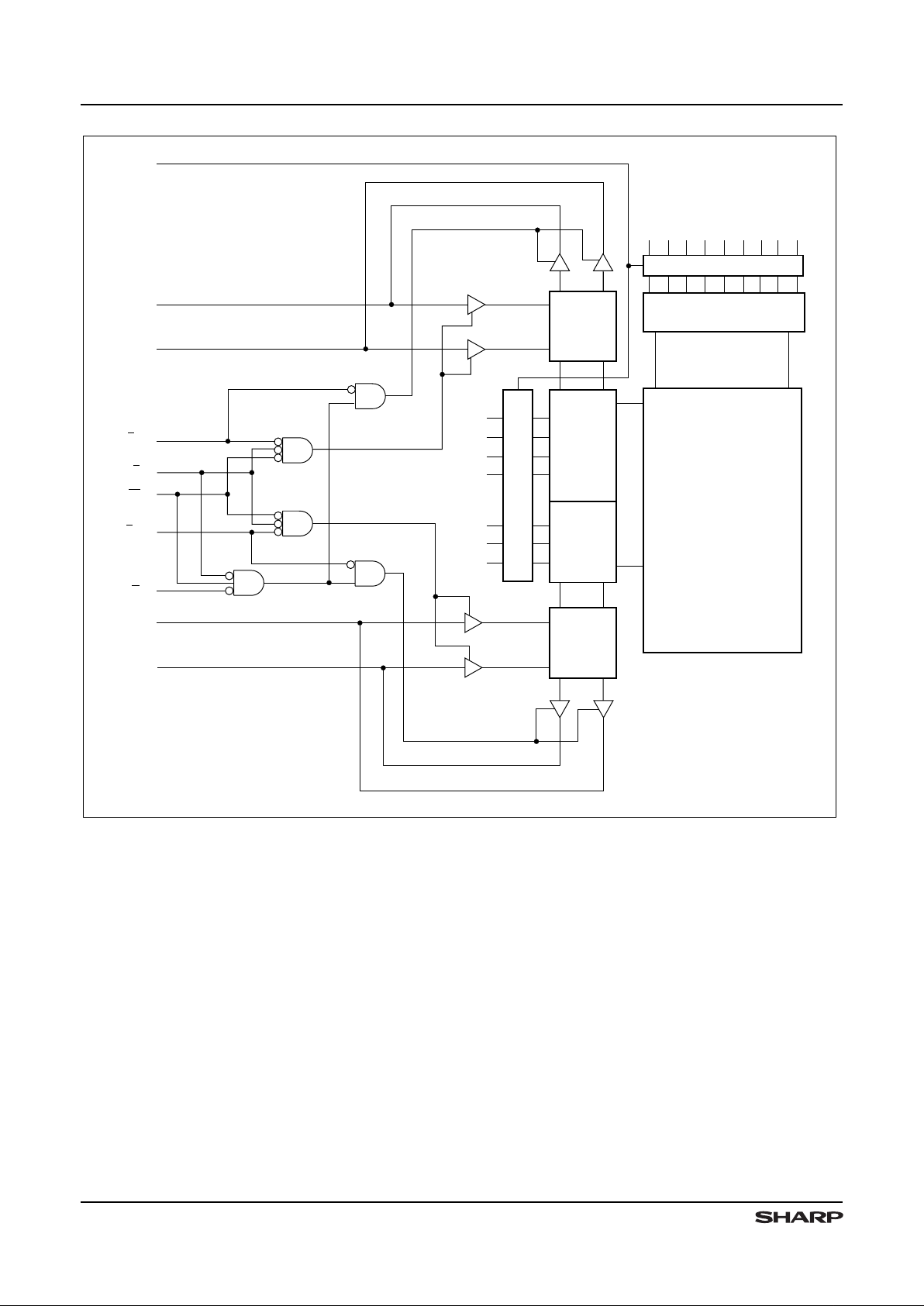
521028-12
. . .. . .
. . .
MEMORY ARRAY
(65,536 x 18)
TRANSPARENT LATCH
ROW DECODE
I/O
CIRCUIT
BLOCK
DECODE
COLUMN
DECODE
I/O
CIRCUIT
TRANSPARENT LATCH
A
15
A
14
A
13
A
12
A
11
A
10
A
9
A8A7A6A5A4A3A2A1A
0
DQ
0
DQ
8
S
L
E
W
S
H
G
DQ
9
ALE
DQ
17
. . .
. . .
. . .
Figure 2. L H521028 A Block Diagr am
LH521028A CMOS 64 K ×× 18 Static RAM
2
Page 3

TRUTH TABLE
ADDRESS E S
H
SLALE G WDQ
0
-DQ
8
DQ9-DQ
17
MODE I
CC
Don’t Care
HXXHXX
High-Z High-Z Standby
I
SB
V alid
LLHHLH
Active High-Z Read
I
CC1
V alid
LHLHLH
High-Z Ac tive Read
I
CC1
V alid
LLLHLH
Activ e Active Read
I
CC1
V alid
LLLHHH
High-Z High-Z Re ad
I
CC1
Don’t Care
LLLLLH
Data Out Dat a O ut Read
I
CC1
V alid
LLHHXL
Data In Don ’t Care Write, low byte
I
CC1
V alid
LHLHXL
Don’t Car e Data In Write , high byte
I
CC1
V alid
LLLHXL
Data In Dat a In Write, both bytes
I
CC1
V alid
LHHHXL
Don’t Car e Do n ’t Care Write, inhibited
I
CC1
Don’t Care
LLLLXL
Data In Dat a In Write, both bytes
I
CC1
NOTE:
X = Don’t Care, L = LOW, H = HIGH
PIN DESCRIPTIONS
PIN SIGNAL PIN SIGNAL PIN SIGNAL PIN SIGNAL
1
V
SS
14
DQ
13
27
V
SS
40
DQ
4
2
V
CC
15
DQ
14
28
V
CC
41
DQ
5
3
S
L
16
V
SS
29
A
8
42
V
SS
4
S
H
17
VCC
30
A
9
43
V
CC
5
E
18
DQ
15
31
A
10
44
DQ
6
6
A
0
19
DQ
16
32
A
11
45
DQ
7
7
A
1
20
DQ
17
33
A
12
46
DQ
8
8
DQ
9
21
A
2
34
DQ
0
47
A
13
9
DQ
10
22
A
3
35
DQ
1
48
A
14
10
V
CC
23
A
4
36
V
CC
49
A
15
11
V
SS 24
A
5 37
V
SS 50
G
12
DQ
11
25
A
6
38
DQ
2
51
ALE
13
DQ
12
26
A
7
39
DQ
3
52
W
CMOS 64K ×× 18 Stati c RAM LH521028A
3
Page 4

PIN DEFINITIONS
V
CC
Positive Supply Voltage Terminals
V
SS
Reference Terminals
A0 – A15Address Bus Input
The Ad dress bu s is decod ed to select one 18- bit word
out of the total 64K wo rds f or Read and Writ e operat ion s.
E Chip Enable Active LOW In put
Chip Enable is used to en able the device for Read and
Write operations. When HIGH, both Read and Write
operations are disabled and the device is in a reduced
power state. When LOW, a Read or Write operation is
enabled.
W Write Enable Active LOW Input
Write Enable is used to select either Read or Write
operations when the device is enabled. When Write
Enable is HIGH and the device is Enabled, a Read
operat ion is select ed. When W rite Enab le is LOW and the
device is enabled, a Write oper ation is selected. A Bytewrite oper ation is available by using th e Byte-select controls.
SH, S
L
Select High Active LOW Inputs
Select Low
The Select High and Select Low signals, in conjunction
with the Chip Enable and W r ite Ena ble signals, allow the
selection of the individual bytes for Read and Write operations. When High, the Select signal will deselect its
byte and prevent Read or Write operations . When the
Select signal is LOW and Chip Enable is LOW, a Read or
Write operation is performed at the location dete rmined
by the c ontent s of the Addr ess bus . When Chip Ena ble is
HIGH, th e Select signals are Don’t Care. S elect Low (SL)
is assigned to DQ0 – DQ8 and Select High (SH) is
assigned to DQ9 – DQ17.
ALE Address Latch Active High Input
Enable
The Addr ess La tch Enable signal is used to c ontrol t he
Tr ans parent lat ches on the Addr ess bus. T he Lat ch es a re
transparent when HIGH and are latched when LOW. If
not required, Address Latch Enable may be tied H IGH,
lea ving the Addr ess bu s in a transpar ent condit ion.
DQ0 – DQ17 Data Bus Input/Output
DQ0 – DQ8 comprise the Low byte, selected by SL,
and DQ9 – DQ17 comprise the High Data byte, selected
by SH. The Data Bus is in a high impedance input mode
during Write operations and standby. The Data bus is in
a low-impe dance output mode dur ing Read oper ations.
G Output Enable Active LOW Input
The Out put Enable signal is u sed t o cont rol the o u tpu t
buffers on the Data Input/Output bus. When G is HIGH,
all output buffers are forced to a high impedance condition. When G is LOW, the output buffers will become
active only during a R ead operation (E and SH / SL are
LO W, W is HIGH).
LH521028A CMOS 64 K ×× 18 Static RAM
4
Page 5

ABSOLUTE MAXIMUM RATINGS
1
PARAMETER RATING
VCC to VSS Potential –0.5 V to 7 V
Input Voltage Range –0.5 V to VCC + 0.5 V
DC Output Current
2
± 40 mA
Storage T e mperature Range –65oC to 150oC
Power Dissipation (Package Limit ) 2 W
NOTES:
1. Stresses greater than those listed under ‘Absolute Maximum Ratings’ may cause permanent damage to the device. This is a st ress rating for
transient condi tions only. Functional operation of the device at these or any other conditions above those indicated in the ‘ O perating Range’
of this specification is not implied. Exposure to absolute maximum rating conditions for extended periods may affect reliability.
2. Outputs should not be shorted for more than 30 seconds. No more than one output should be shorted at any time.
OPERATING RANGES
SYMBOL PARAMETER MIN TYP MAX UNIT
T
A
T em perat ure, Ambi ent
070
o
C
V
CC
Sup ply V oltag e
4.5 5.0 5.5 V
V
SS
Sup ply V oltag e
000V
V
IL
Logic ‘0 ’ Input V olta ge
1
–0.5 0.8 V
V
IH
Logic ‘1 ’ Input V olta ge
2.2 VCC + 0.5 V
NOTE:
1. Negative undershoot of up to 3.0 V is permitted once per cycle.
DC ELECTRICAL CHARACTERIS TICS
SYMBOL PARAMETER TEST CONDITIONS MIN TYP MAX UNIT
I
CC1
Oper ating Curr ent
1
t
CYCLE
= minimum
300 mA
I
SB1
Standb y Current
E ≥ VCC – 0.2 V
VIN ≥ VCC – 0.2 V o r VIN ≤ 0.2 V
f = 0
4mA
I
SB2
Standb y Current
E ≥ V
IH
VIN = VIH or V
IL
50 mA
I
LI
Inpu t Lea kage Cur ren t VIN = 0 V to V
CC
–2 2
µA
I
LO
I/O Leakage Current VIN = 0 V to V
CC
–2 2
µA
V
OH
Out put Hig h V oltage IOH = –4.0 mA
2.4 V
V
OL
Output Low Voltag e IOL = 8.0 m A
0.4 V
NOTE:
1. I
CC
is dependent upon output loading and cycle rates. Specified values are with outputs open.
CMOS 64K ×× 18 Stati c RAM LH521028A
5
Page 6

AC TEST CONDITIONS
PARAMETER RATING
Input Pulse Levels
V
SS
to 3 V
Input Rise and Fall T imes
5 ns
Input and Output T iming Ref. Le vels
1.5 V
Output Load , Timin g T es ts
Figure 3
CAPACITANCE
1,2
PARAMETER RATING
C
IN
(Input Capacit ance)
5 pF
C
DQ
(I/O Capacit ance)
7 pF
NOTES:
1. Capacitances are maximum values at 25
o
C measured at 1.0 MHz
with V
Bias
= 0 V and VCC = 5.0 V.
2. Guaranteed but not tested.
+5 V
DQ PINS
521028-13
* INCLUDES JIG AND SCOPE CAPACITANCES
255 Ω
C
LOAD
=30 pF *
480 Ω
Figure 3. Output Load Cir cui t
LH521028A CMOS 64 K ×× 18 Static RAM
6
Page 7

AC ELECTRICAL CHARACTERIS TIC S
1
(Over Operatin g Range)
SYMBOL DESCRIPTION
–15 –17 –20 –25 –35
UNITS
MIN MAX MIN MAX MIN MAX MIN MAX MIN MAX
READ CYCLE
t
RC
Read Cycle Timing 15 17 20 25 35 ns
t
AA
Address Acce ss T im e
15 17 20 25 35 ns
t
ASL
Address Setup to Latch Enable 22222 ns
t
AHL
Address Hold from Latch Enable 33444 ns
t
LEA
Latch Enable to Data Valid 16 18 21 26 36 ns
t
LHM
Latch Enab le High Puls e Width 55555 ns
t
OH
Output Hold fro m Addr ess Cha nge 44444 ns
t
LH
Output Hold from Latch High 4.5 4.5 4.5 4.5 4.5 ns
t
EA
E Low to Val id Data 15 17 20 25 35 ns
t
ELZ
E Low to Output Active
2,3
33333 ns
t
EHZ
E High to Output High -Z
2,3
9 10101220ns
t
SA
S Low to Val id Data 7 8 10 12 20 ns
t
SLZ
S Low to Output Active
2,3
22233 ns
t
SHZ
S High to Output High -Z
2,3
10 10 10 12 20 ns
t
GA
G Low to Va lid Data 7 8 9 12 20 ns
t
GLZ
G Low to Output Activ e
2,3
00000 ns
t
GHZ
G High to Output Hig h-Z
2,3
7 8 8 10 20 ns
t
RCS
Read Setup from W High 00000 ns
t
RCH
Read Hold from W Low 0000 0 ns
t
PU
E LOW to Power Up Time
3
00000 ns
t
PD
E HIGH to Power Down Time
3
15 17 20 25 35 ns
t
WA
Access T ime Fro m Wri te Enab le HIGH 18 20 20 25 35 ns
WRITE CYCLE
t
WC
Write Cycle Time 15 17 20 25 35 ns
t
EW
E Low to End of Write 11 12 13 20 30 ns
t
SW
S LOW to End of Write 7 8 10 20 30 ns
t
AW
Address Valid to End of Write 11 12 13 20 30 ns
t
AS
Address Setup to Start of Write 00000 ns
t
AH
Address Hold from End of Write 00000 ns
t
ASL
Address Setup to Latch Enable 22222 ns
t
AHL
Address Hold from Latch Enable 33444 ns
t
LHW
Latch Hold from W High 00000 ns
t
LHM
Latch Enab le HIGH Pul se Width 55555 ns
t
WP
W Pulse Width 11 12 13 20 30 ns
t
DW
Input Data Setup Time 7 8 9 10 15 ns
t
DH
Input Dat a Hold T ime 00000 ns
t
WHZ
W Low to Output High- Z
2,3
7 8 8 10 14 ns
t
WLZ
W High to Output Active
2,3
33333 ns
NOTES:
1. AC Electrical Characteristics specified at ‘AC Test Conditions’ levels.
2. Active output to High-Z and High-Z to output active tests specified for a ±500 mV transitio n from steady state levels into the test load.
C
Load
= 5 pF.
3. Guaranteed but not tested.
CMOS 64K ×× 18 Stati c RAM LH521028A
7
Page 8

TIMING DIAGRAMS – READ CYCLE
Read Cycle No. 1
(Unlatched Address Controlled Read)
Chip is in Read Mode: ALE is HIGH (transparent
mode), E and G are LOW. Read cycle timing is referenced
from when all addresses are sta ble unt i l the fir st addr ess
transition. Foll owing a W-controlled Wr ite cycle, tWA and
tAA must both be satisfied to ensure valid data. Crosshatched portion of Data Out imp l ies that d ata line s ar e in
the Low-Z sta te but the dat a is n ot guarante ed to be val id
until tAA.
Read Cycle No. 2
(Unlatched Chip Enable Controlled Read)
Chip is in Read Mode: ALE is HIGH (transparent
mode). Read cy cle timing is referenced from when E, S
,
and G are stable until the first address transition. Crosshat ched po rtion of Data Out implies that data lines are in
the L ow-Z state bu t the data is n ot guar anteed to be v alid .
t
RC
VALID ADDRESS
t
AA
t
OH
VALID DATA
ADDRESS
DQ
521028-2
PREVIOUS DATA
t
WA
W
Figur e 4. Read Cycle No. 1
t
SLZ
t
GLZ
t
ELZ
t
SA
VALID DATA
t
GHZ
SL, S
H
G
DQ
VALID ADDRESS
ADDRESS
W
t
RCS
t
RCH
t
EA
t
EHZ
t
GA
t
SHZ
E
521028-3
Figure 5. Read Cycle No. 2
LH521028A CMOS 64 K ×× 18 Static RAM
8
Page 9

TIMING DIAGRAMS – RE AD CYCLE (cont’ d)
Read Cycle No. 3
(Latched Address Controlled Read)
Chip is in Read Mode: W is HIGH, E, SH, SL and G ar e
LOW. Bot h tAA and t
LEA
must be met before valid data is
available. I f t he address is valid prior to the rising edg e of
ALE, then the access time is t
LEA
. If the address is valid
after ALE is HIGH (or if ALE is tied HIGH) then the access
time is tAA. Crosshatc hed portion of Data Out im plies that
data lines are in the Low-Z state but the data is not
guaranteed to be valid until tAA.
ADDRESS
DQ
t
ASL
521028-4
E, SH, S
L
VALID ADDRESS
PREVIOUS DATA VALID DATA
t
LHM
t
AA
t
LEA
t
AHL
t
LH
ALE
Figure 6. Read Cycle No. 3
CMOS 64K ×× 18 Stati c RAM LH521028A
9
Page 10

TIMING DIAGRAMS – RE AD CYCLE (cont’ d)
Read Cycle No. 4
Chip is in Read Mo de: Timing illustrated for the case
when add resses ar e va lid b efo re E goes LO W. Dat a Out
is not specifie d t o be valid until tEA, tSA and tGA, but may
become active as early as t
ELZ
, t
SLZ
or t
GLZ
.
t
AHL
t
ASL
VALID ADDRESS
ADDRESS
W
t
LHM
t
LEA
t
EA
t
RCS
t
RCH
t
SA
t
RC
t
SLZ
t
GLZ
t
ELZ
t
GA
VALID DATA
t
GHZ
t
EHZ
ALE
E
S
L
, S
H
G
DQ
521028-5
Figur e 7. Read Cycle No. 4
LH521028A CMOS 64 K ×× 18 Static RAM
10
Page 11

TIMING DI AGRAMS – WRITE CYCLE
Addresses must be stable during unlatched Write
cycles . The out put s will remain in th e Hig h-Z state if W is
LOW when E and SH / SL go LOW. If G is HIGH, the
outputs w ill remain in the High-Z sta te. Although these
examples illustrate timing with G active, it is recommended t hat G be held HIG H for al l Write cycles. This w ill
prevent the LH521028’s outputs from becoming active,
preventing bus contention, thereby reducing system
noise.
Write Cycle No. 1 (Unlatched W Controll e d Wri te)
Chip is selected: E, G, and SH / SL are LOW, ALE is
High. Using only W to control Writ e cycles may not off er
the best performance since both t
WHZ
and tDW timing
specifications must be met.
Write Cycle No. 2 (E, SL, SH Controlled Write)
G is LOW. DQ lines may transition to Low-Z if the falling
edg e of W oc curs after the falling e dge of E, SH/SL if G is
LOW.
t
WC
t
AW
t
WP
t
DW
t
AH
t
WLZ
t
WHZ
t
AS
t
DH
PREVIOUS OUTPUT
VALID DATA
VALID ADDRESS
521028-6
W
ADDRESS
DQ
Figure 8. Write Cycle No. 1
t
EW
ADDRESS
E, S
L
, S
H
DQ
VALID DATA
VALID ADDRESS
t
WC
t
WP
t
AH
t
AS
t
ELZ
t
WHZ
t
DW
t
DH
W
521028-7
Figure 9. Write Cycle No. 2
CMOS 64K ×× 18 Stati c RAM LH521028A
11
Page 12

TIMING DI AGRAMS – WRITE CYCLE (con t’d)
Write Cycle No. 3 (Latched W Controlled Wri te)
Ch ip is s e le cted: E, G, and SH / SL are LOW.
Write Cycle No. 4 (E Controlled)
G is LOW . DQ lines may transition to Low-Z if the falling
edge of W occurs after the falling edg es of E and SH/SL.
t
WC
t
LHM
t
DW
t
AHL
t
ASL
t
AW
t
WLZ
521028-8
t
LHW
t
WP
t
AS
t
WHZ
VALID DATA
t
DH
PREVIOUS OUTPUT
ALE
ADDRESS
W
DQ
VALID ADDRESS
Figure 10. Wr ite Cycl e No. 3
VALID DATA
t
WC
t
LHM
t
WP
t
DW
t
AHL
t
AS
t
DH
t
WHZ
t
ELZ
t
ASL
t
EW
t
LHW
t
SLZ
521028-9
ALE
ADDRESS
E, S
H
/ S
L
W
DQ
VALID ADDRESS
Figure 1 1. Wri te Cycle No. 4
LH521028A CMOS 64 K ×× 18 Static RAM
12
Page 13

BYTE OPERATIONS
Byte Read Descri ption (Figure 12)
To read individual bytes, the device must be enabled
(E is LOW), W must be HIGH, the outputs must be
enabled (G is LOW) and the addresses must be either
stable or latched with ALE. Figure 12 is one example of
the byte read capabilities of this device. The example
shows two read operations. The fir st is a re ad of the high
byte of the current memory location and the se c ond is a
read of the low byt e of the memory location.
(1) At the beginning of the cycle both SL and SH are
HIGH .
(2) SH goes LOW initiating a Read on the upper byte
DQ
H(9-17)
. SL remains HIGH ke eping t he lower byte
DQ
L(0-8)
disabled and in a high-impedanc e mode.
(3) SL goes L OW activat ing DQ
L(0-8)
.V alid data is avail-
able in tSA following SL going LOW.
(4) When SH goes HIGH, DQ
H(9-17)
remains valid for t
SH Z
before retur ning to a high-im peda nce cond ition.
(5) Finally, the Read for the lower byte is terminated by
deasserting SL (HIGH). DQ
L(0-8)
remains active for
t
SHZ
following SL going HIGH.
ADDRESS
VALID DATA
VALID DATA
ALE
G
S
L
S
H
DQ
L (0-8)
DQ
H (9-17)
(1) (2) (3) (4) (5)
521028-10
VALID ADDRESS
Figur e 12. Byte Read (E is LOW and W is HIGH)
CMOS 64K ×× 18 Stati c RAM LH521028A
13
Page 14

BYTE OPERATIONS (cont’d)
Byte Wri te Description (Figure 13)
T o do indiv idual byte-wr ite operations , the device must
be enabled (E is LOW, G is don’t care) and addresses
must be either stable or latched. Figure 13 is one example
of the byte-write capabilities of this device. The diagram
shows two write operations with unlatched addresses.
The first is a write to the low byte of memory location N
and the second is a write to the high byte of memory
location M.
(1) W goes LOW while SL and SH remain HIGH.
(2) SL goes LOW initiating a Write into the lower byte
DQ
L(0-8)
of memory location N. SH remains HIGH
preventing a Write into the upper byte DQ
L(9-17)
of
memory location N.
(3) SL now goes HIGH terminating the Write operation
on the lower byte of memory location N.
(4) Address N is changed t o M.
(5) The W rite op erat ion is now initiated on the upper byte
DQ
H(9-17 )
by bringing SH LOW. SL remains HIGH
preventing a Write operation from occurring in the
lower byte DQ
L(0-8)
of mem ory locat ion N+ 1.
(6) SH now goes HIGH terminating the Write operation
on the upper byte of address M.
(7) W goes HIGH, ending the Write opera tion.
(1) (2) (3)
VALID ADDRESS N VALID ADDRESS M
DATA IN (N)
DATA IN (M)
(7)(6)(4) (5)
ADDRESS
ALE
W
S
L
S
H
DQ
L (0-8)
DQ
H (9-17)
521028-11
Figure 13. By te Wri te (E is LOW)
LH521028A CMOS 64 K ×× 18 Static RAM
14
Page 15

PACKAGE DIAGRAM
52PLCC-A
19.69 [0.775]
18.67 [0.735]
19.69 [0.775]
18.67 [0.735]
20.57 [0.810]
19.56 [0.770]
20.57 [0.810]
19.56 [0.770]
18.8 [0.740]
17.78 [0.700]
MAXIMUM LIMIT
MINIMUM LIMIT
DIMENSIONS IN MM [INCHES]
1.27 [0.050]
TYP.
.58 [0.023]
.33 [0.013]
0.76 [0.030]
1.38 [0.015]
4.06 [0.160]
3.56 [0.140]
0.10 [0.004]
52-Pi n PLC C
15
17
20
25
35
52-pin, Plastic Leaded Chip Carrier (PLCC52-P-750)
LH521028A
Device Type
U
Package
- ##
Speed
521028AM
CMOS 64K x 18 Static RAM
Example: LH521028AU-15 (CMOS 64K x 18 Static RAM, 15 ns, 52-pin, Plastic Leaded Chip Carrier)
Access Time (ns)
ORDERING INFO RMATION
CMOS 64K ×× 18 Stati c RAM LH521028A
15
 Loading...