

Page 1
LH5164AZ8
CMOS 64K (8K × 8 ) Static RAM
FEATURES
•• 8,192 × 8 bit organ izatio n
•• Acces s time:
200 ns (V
= 3.0 V MAX.)
CC
•• Power co nsump tion:
Operati ng:
60 mW (MAX.) @ 3 V
Standb y (to 60° C):
3 µW (MAX.) @ 3 V
Data hold
0.6 µA (V
= 3 V, TA = 60°C)
CC
•• Operating voltage range:
3.0 V to 3.6 V
•• Wide operating te mperature range:
-30 to 60° C
•• Ful ly-static operation
•• TTL compatibl e I/ O
•• Three-state outpu ts
•• Pa ckage : 28-pin , 450-mil SOP
DESCRIP TION
The LH5164AZ8 is a static RAM organized as
8,192 × 8 bits. It is fa bricated using silicon-gate CMOS
process technology.
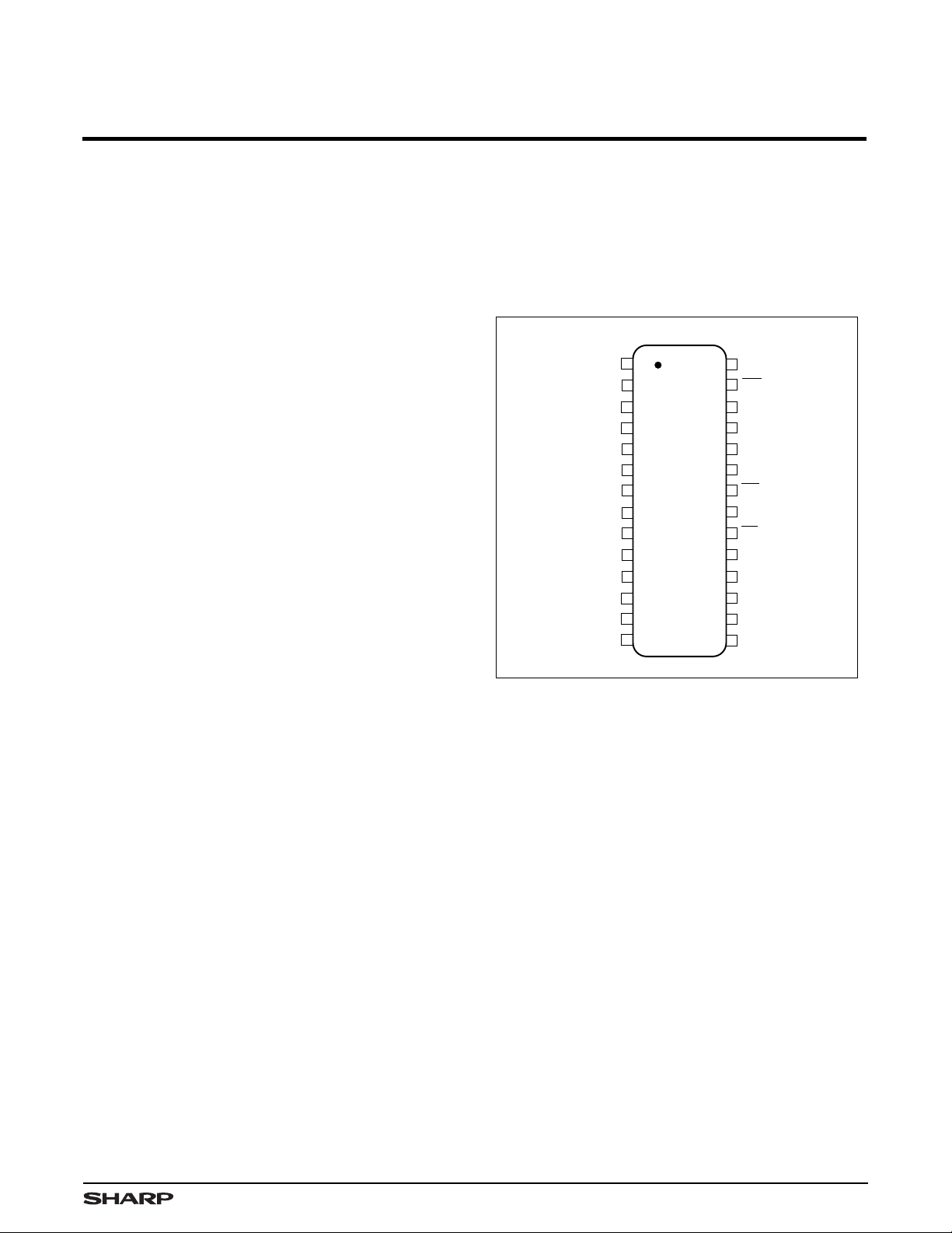
PIN CONNECTI ONS
28-PIN SOP
NC
A
A
A
A
A
A
A
A
A
I/O
I/O
I/O
GND
1
2
12
3
7
4
6
5
5
6
4
7
3
8
2
9
1
10
0
11
1
12
2
13
3
14
28
27
26
25
24
23
22
21
20
19
18
17
16
15
Figure 1. Pin Connections for SOP Package
V
WE
CE
A
A
A
OE
A
CE
I/O
I/O
I/O
I/O
I/O
TOP VIEW
CC
2
8
9
11
10
1
8
7
6
5
4
5164AZ8-1
1
Page 2
LH5164A Z8 CMOS 64K (8 K ×× 8) Static RAM
A
24
9
25
A
8
2
A
I/O
I/O
I/O
I/O
I/O
I/O
I/O
I/O
12
A
3
7
A
4
6
A
5
5
A
6
4
A
7
3
11
1
12
2
13
3
15
4
16
5
17
6
18
7
19
8
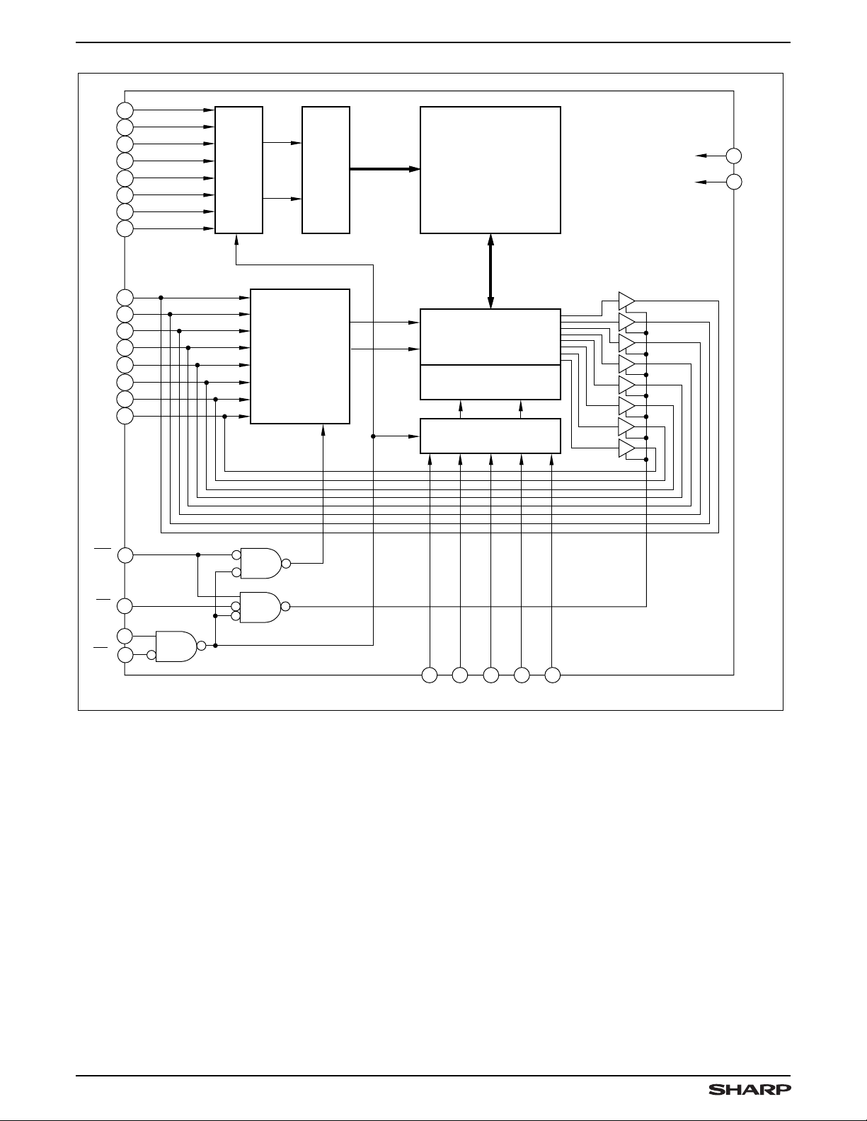
BUFFERS
ROW ADDRESS
INPUT
DATA
CONTROL
ROW SELECT
MEMORY
ARRAY
(256 x 256)
COLUMN I/O
CIRCUITS
COLUMN SELECT
COLUMN ADDRESS
BUFFERS
28
14
V
CC
GND
27
WE
22
OE
26
CE
2
CE
20
1
PIN DESCRIPTION
SIGNA L PIN N AME
A0 - A
12
CE1 - CE
WE Write E na ble inp ut
OE Outpu t E nab le inp ut
Addre ss inputs
Chip Ena ble in put
2
8239
A2A1A0A
10 21
A
11
Figure 2. LH5164AZ8 Block Diagram
SIGNAL PIN NAME
I/O1 - I/O
8
V
CC
GND Ground
NC Non co nne cti on
10
Data i npu ts and ou tpu ts
Power sup ply
5164AZ8-2
2
Page 3

CMOS 64K (8K ×× 8) Static RAM LH5164AZ8
TRUTH TABLE
CE
1
CE
2
WE OE MODE I/O1 - I/O
SUPPLY CURRENT NOTE
8
H X X X Standby High-Z Standby (ISB)1
X L X X Standby High-Z Standby (ISB)1
L H L X Write D
L H H L Read D
IN
OUT
L H H H Output deselect High-Z Operating (I
NOTE:
1. X = H or L
Operating (ICC)1
Operating (ICC)
)
CC
ABSOLUTE MAXIMUM RATINGS
PARAMETER SYMBOL RATING UNIT NOTE
Suppl y v olt age V
Input vol tage V
CC
IN
Operating temperature Topr -30 to +60
Storage temperature Tstg -65 to +150
NOTE:
1. The maximum applicable voltage on any pin with respec t to GND.
-0.3 to +7.0 V 1
-0.3 to VCC + 0.3 V 1
°C
°C
RECOMMENDED OPERATING CONDITIONS (TA = -30 to +60°C)
PARAMETER SYMBOL MIN. TYP. MAX. UNIT
Suppl y v olt age
Input vol tage
(V
= 3.0 to 3.6 V)
CC
V
CC
V
IH
V
IL
3.0 3.6 V
VCC - 0.5 VCC + 0.3 V
-0.3 0.2 V
DC CHARACTERISTICS (TA = -30 to +60°C, VCC = 3.0 to 3.6 V)
ADD TABLE
NOTE:
1.
should be ≥ VCC - 0.2 V or ≤ 0.2 V.
CE
2
3
Page 4

LH5164A Z8 CMOS 64K (8 K ×× 8) Static RAM
AC CHARACTERISTICS
(1) READ CYCLE (T
PARAMETER SYMBOL MIN. MAX. UNIT
Read cycle t
Addres s a cc ess ti me t
Chip e nab le
acces s t ime
Output en abl e a cce ss tim e t
Output ho ld time t
Chip e nab le to
output in Lo w-Z
Output en abl e t o ou tpu t i n L ow- Z t
Chip e nab le to
output in Hi gh- Z
Output disable to outp ut in High-Z
= -30 to +60°C, VCC = 3.0 to 3.6 V)
A
RC
AA
(
CE1)t
(CE
)t
2
(
CE1)t
)t
(CE
2
(
CE1)t
(CE
)t
2
ACE1
ACE2
OE
OH
LZ1
LZ2
OLZ
HZ1
HZ2
t
OHZ
200 ns
200 ns
200 ns
200 ns
150 ns
10 ns
20 ns
20 ns
10 ns
060ns
060ns
040ns
(2) WRITE CYCLE (TA = -30 to +60°C, VCC = 3.0 to 3.6 V)
PARAMETER SYMBOL MIN. MAX. UNIT
Write c ycl e t ime t
Chip e nab le to end of write t
Addres s v al id t o e nd of writ e t
Addres s s etu p t ime t
Write p uls e w idt h t
Write re co ver y ti me t
Data v ali d t o e nd of w rit e
Data h old ti me
Output ac tiv e f rom end of wri te
WE to out put in Hig h-Z t
OE to out put in Hig h-Z t
WC
CW
AW
AS
WP
WR
t
DW
t
DH
t
OW
WZ
OHZ
200 ns
180 ns
180 ns
0ns
150 ns
0ns
100 ns
0ns
20 ns
060ns
040ns
AC TEST CONDITIONS
PARAMETER MODE
Input voltage amplitude 0 to V
CC
Input rise/fall time 10 ns
Timing re fer enc e l eve l 1.5 V
Output lo ad con dit ion s No load
CAPACITANCE (TA = 25°C, f = 1 MHz)
PARAMETER SYMBOL CONDITIONS MIN. TYP. MAX. UNIT
Input cap acitan ce
Input/ out put ca pac ita nce C
NOTE:
This parameter is samp led and not production tested.
C
IN
I/O
4
VIN = 0 V 7 pF
V
= 0 V 10 pF
I/O
Page 5

CMOS 64K (8K ×× 8) Static RAM LH5164AZ8
DATA RETENTION CHARACTERISTICS (TA = -30 to +60°C)
PARAMETER SYMBOL CONDITIONS MIN. MAX. UNIT NOTE
Data r ete nti on s up ply vo lta ge V
Data r ete nti on s up ply cu rren t I
Chip d isa ble to da ta rete nti on t
Recov ery tim e t
NOTES:
1.
should be ≥ V
CE
2
= Read cycle time
2. t
RC
- 0.2 V or ≤ 0.2 V.
CCDR
ADDRESS
CCDR
CCDR
CDR
R
V
CE
CE1 ≥ V
CE1 ≥ V
= 3.0 V,
CCDR
≤ 0.2 V or
2
CCDR
t
AA
t
ACE1
CE2 ≤ 0.2 V or
– 0.2 V
CCDR
– 0.2 V
t
RC
T
= 25°C
A
T
= 60°C
A
2.0 5.5 V 1
0.2
µA
0.6 1
0ns
t
RC
ns 2
CE
1
CE
2
OE
D
OUT
NOTE: WE is "HIGH" level during the read cycle.
t
LZ1
t
ACE2
t
LZ2
t
OE
t
OLZ
DATA VALID
Figure 3. Read Cycle
t
HZ1
t
HZ2
t
OHZ
t
OH
5164AZ8-3
5
Page 6

LH5164A Z8 CMOS 64K (8 K ×× 8) Static RAM
t
WC
ADDRESS
OE
t
AW
t
WR
(NOTE 4)
CE
t
CW
(NOTE 2)
1
t
WR
t
WR
CE
t
CW
2
t
AS
(NOTE 3)
t
WP
(NOTE 1)
WE
t
OHZ
D
OUT
t
DW
D
IN
(NOTE 5)
t
DH
DATA VALID
NOTES:
1. The writing occurs during an overlapping period of CE1 = "LOW," CE2 = "HIGH," and WE = "LOW" (tWP).
2. t
is defined as the time from the last occuring transit, either CE1 LOW transit or CE2 HIGH transit,
CW
to the time when the writing is finished.
3. t
is defined as the time from address change to writing start.
AS
4. t
is defined as the time from writing finish to address change.
WR
5. The input signals of opposite phase to the outputs must not be applied while I/O pins are in the output state.
5164AZ8-4
Figure 4. Write Cycle
6
Page 7

CMOS 64K (8K ×× 8) Static RAM LH5164AZ8
t
WC
ADDRESS
t
AW
(NOTE 4)
t
WR
t
WR
CE
CE
t
CW
(NOTE 2)
1
t
CW
2
t
AS
(NOTE 3)
t
WP
(NOTE 1)
t
WR
WE
t
WZ
(NOTE 6)
D
OUT
t
DW
D
IN
(NOTE 5)
t
OW
(NOTE 7)
t
DH
DATA VALID
NOTES:
1. The writing occurs during an overlapping period of CE
is defined as the time from the last occuring transit, either CE1 LOW transit or CE2 HIGH transit,
2. t
CW
to the time when the writing is finished.
is defined as the time from address change to writing start.
3. t
AS
is defined as the time from writing finish to address change.
4. t
WR
5. The input signals of opposite phase to the outputs must not be applied while I/O pins are in the output state.
6. If CE
remain high-impedance.
7. If CE
remain high-impedance.
LOW transit or CE2 HIGH transit occurs at the same time or after WE LOW transit, the output will
1
HIGH transit or CE2 LOW transit occurs at the same time or before WE HIGH transit, the output will
1
= "LOW," CE2 = "HIGH," and WE = "LOW" (tWP).
1
5164AZ8-5
Figure 5. OE Low Fixed
7
Page 8

LH5164A Z8 CMOS 64K (8 K ×× 8) Static RAM
CE
CONTROL (NOTE)
1
CE2 CONTROL
V
CC
CE2
DATA HOLD MODE
V
CC
2.5 V
V
- 0.2 V
CC
V
CCDR
CE
1
t
CDR
CE
1
≥ V
CCDR
- 0.2 V
t
RDR
0 V
DATA HOLD MODE
V
2.5 V
CCDR
t
CDR
t
RDR
0.2 V
0 V
CE
0.2 V
≥
2
NOTE: To control the data hold mode at CE
during the data hold mode.
, fix the input level of CE2 between V
1
CCDR
to V
CCDR
Figure 6. Low Voltage Data Retention
- 0.2 V or 0 V to 0.2 V
5164AZ8-6
8
Page 9

CMOS 64K (8K ×× 8) Static RAM LH5164AZ8
PACKAGE DIAGRAM
28SOP (SOP028-P-0450)
1.27 [0.050]
0.50 [0.020]
0.30 [0.012]
28 15
TYP.
1.70 [0.067]
18.20 [0.717]
17.80 [0.701]
DIMENSIONS IN MM [INCHES]
141
0.15 [0.006]
MAXIMUM LIMIT
MINIMUM LIMIT
8.80 [0.346]
8.40 [0.331]
1.70 [0.067]
1.025 [0.040]
1.025 [0.040]
12.40 [0.488]
11.60 [0.457]
0.20 [0.008]
0.00 [0.000]
28-pin, 450-mil SOP
10.60 [0.417]
0.20 [0.008]
0.10 [0.004]
2.40 [0.094]
2.00 [0.079]
28SOP
ORDERING INFORMATI ON
LH5164AZ8
Device Type
CMOS 64K (8K x 8) Static RAM
Example: LH5164AZ8 (CMOS 64K (8K x 8) Static RAM, 200 ns, 28-pin, 450-mil SOP)
5164AZ8-7
9
 Loading...