

Page 1
LH5164ASH
CMOS 6 4K (8 K × 8) S tatic RA M
FEATURES
•• 8,192 × 8 bit orga niza ti on
•• Access time: 500 ns (MAX.)
•• Power consu mption :
Operating:
60 mW (MAX.) @ 3 V
Standb y:
3 µW (MAX.) @ 70°C @ 3 V
9 µW (MAX.) @ 85°C @ 3 V
•• Fully-static operatio n
•• Three-state outputs
•• Wide o pera tin g voltage range:
2.5 V to 5.5 V
•• TTL compatible I/O
•• Wide temp . range
t
OPR
: -40 to +85°C
•• Packages:
28-pi n , 450 -mil S OP
28-pi n , 8 × 13 mm
2
TSOP (Type I)
DESCRIPTION
The LH5164ASH is a static RAM organized as
8,192 × 8 bits. It is fabricated using silicon-gate CMOS
process technology.
It is desi gned for 2.5 to 5.5 V low voltage operation
and wide temperature range from -40 to +85°C.
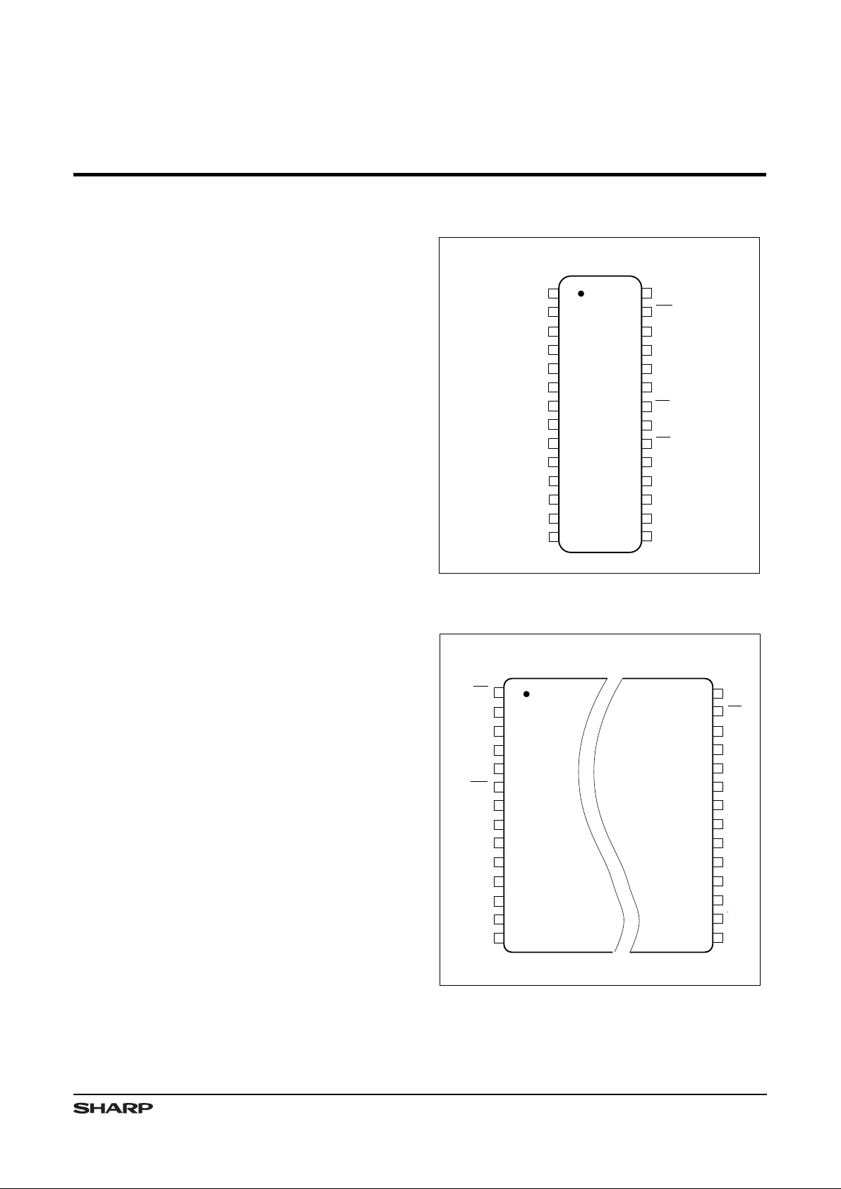
PIN CONNECTIONS
1
2
3
4
7
8
A
2
A
5
26
25
24
23
22
21
18
15
A
7
A
6
5
6
A
3
A
4
20
19
A
12
GND
A
8
A
11
A
10
CE
1
9
10
11
28
27
WE
A
1
V
CC
12
17
16
A
0
I/O
1
A
9
13
14
NC
OE
I/O
2
I/O
3
I/O
7
I/O
6
I/O
5
I/O
4
I/O
8
CE
2
5164ASH-1
TOP VIEW
28-PIN SOP
Figure 1. Pin Connections for SOP Package
2
3
4
5
6
9
10
7
8
A
11
11
1
28
27
26
25
22
21
24
23
20
19
A
10
28-PIN TSOP (Type I)
12
13
14
17
16
18
15
OE
A
8
A
9
CE
2
WE
A
12
NC
I/O
3
I/O
2
A
1
I/O
8
CE
1
I/O
6
I/O
7
GND
I/O
5
I/O
4
I/O
1
A
0
5164ASH-8
V
CC
A
7
A
6
A
5
A
4
A
3
A
2
TOP VIEW
Figure 2. Pin Connect ions for TSOP Package
1
Page 2
I/O
8
A
8
A
9
A
12
25
24
2
11
15
18
5164ASH-2
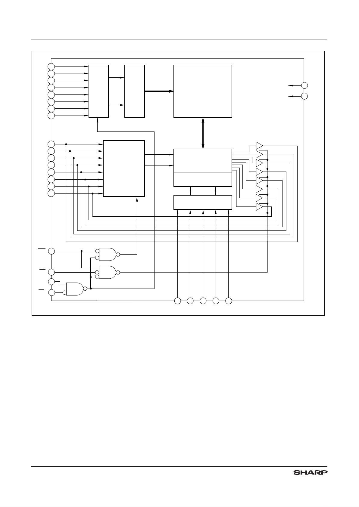
MEMORY
ARRAY
(256 x 256)
13
17
12
16
A
7
3
ROW ADDRESS
BUFFERS
WE
A
6
4
A
5
5
27
A
4
6
ROW DECODERS
I/O
CIRCUITS
COLUMN DECODERS
V
CC
GND
OE
I/O
7
I/O
6
I/O
5
I/O
4
I/O
3
I/O
2
I/O
1
22
19
COLUMN ADDRESS
BUFFERS
10
A
0A1A2A10
21
9
8
28
14
A
3
7
CE
1
20
26
CE
2
DATA CONTROL
A
11
23
Figure 3. LH5164ASH Block Diagram
PIN DESCRIPTION
SIGNA L PIN N AME
A0 - A
12
Addre ss inputs
CE1 - CE
2
Chip Ena ble in put
WE Write E na ble inp ut
OE Outpu t E nab le inp ut
SIGNAL PIN NAME
I/O1 - I/O
8
Data i npu ts and ou tpu ts
V
CC
Power sup ply
GND Ground
NC No connec tion
LH5164A SH CMOS 64K (8 K × 8) Static RAM
2
Page 3

TRUTH TABLE
CE
1
CE
2
WE OE MODE I/O1 - I/O
8
SUPPLY CURRENT NOTE
H X X X Deselect High-Z Standby (ISB)1
X L X X Deselect High-Z Standby (I
SB
)1
L H L X Write D
IN
Operating (ICC)1
L H H L Read D
OUT
Operating (ICC)
L H H H Output disable High-Z Operating (I
CC
)
NOTE:
1. X = H or L
ABSOLUTE MAXIMUM RATINGS
PARAMETER SYMBOL RATING UNIT NOTE
Suppl y v olt age V
CC
-0.3 to +7.0 V 1
Input vol tage V
IN
-0.3 to VCC +0.3 V 1, 2
Operat ing te mpe ratu re
Topr -40 to +85 °C
Storag e t emp era ture
Tstg -65 to +150 °C
NOTES:
1. The maximum appl ic able voltage on any pin with respect to GND.
2.
VIN (MIN.) = -3.0 V f or pulse width ≤50 ns.
RECOMMENDED OPERATING CONDITIONS (TA = -40 to +85°C)
PARAMETER SYMBOL MIN. TYP. MAX. UNIT NOTE
Suppl y v olt age V
CC
2.5 3.0 5.5 V
Input vol tage
(V
CC
= 2.5 to 4.5 V)
V
IH
VCC - 0.5 VCC + 0.3 V
V
IL
-0.3 0.2 V 1
Input vol tage
(VCC = 4.5 to 5.5 V)
V
IH
2.2 VCC + 0.3 V
V
IL
-0.3 0.8 V
NOTE:
1.
V
IN
(MIN.) = -3.0 V f or pulse width ≤50 ns.
DC CHARACTERISTICS (TA = -40 to +85°C, VCC = 2.5 to 5.5 V)
PARAMETER SYMBOL CONDITIONS MIN. MAX. UNIT NOTE
Input lea kag e c urr ent I
LI
VIN = 0 to V
CC
-1.0 1.0
µA
Output le aka ge
curren t
I
LO
CE1 = VIH or CE2 = V
IL
or OE = VIH or WE = V
IL
V
I/O
= 0 to V
CC
-1.0 1.0
µA
Operat ing su ppl y
curren t
I
CC
CE1 = 0.2 V, VIN = 0.2 V or
V
CC
- 0.2 V
CE
2
= VCC - 0.2 V,
Output open
t
CYCLE
=
500 ns
20
mA
CE1 = 0.2 V, VIN = 0.2 V or
V
CC
- 0.2 V
CE
2
= VCC - 0.2 V,
Output open
t
CYCLE
=
1.0 µs
10
CE1 = 0.2 V, VIN = 0.2 V or
V
CC
- 0.2 V
CE
2
= VCC - 0.2 V,
Output open, V
CC
= 3.3 V
t
CYCLE
=
1.0 µs
8
Standb y c urr ent
I
SB
CE2 ≤ 0.2 V or
CE1 ≥ VCC - 0.2 V
T
A
≤ +70°C
1.0
µA
1
T
A
≤ +85°C
3.0
I
SB 1
CE1 = V
IH or CE2
= V
IL
5mA
Output Lo w v olt age V
OL
IOL = 500 µA
0.5 V
Output Hi gh vol tag e V
OH
IOH = -500 µA
V
CC
- 0.5 V 2
NOTES:
1.
CE
2
should be ≥ VCC - 0.2 V or ≤ 0.2 V when CE1 ≥ VCC - 0.2
V.
2. V
OH
is 4.5 V (M in.) at VCC > 5 V.
CMOS 64K (8K × 8) Static RAM LH5164ASH
3
Page 4

AC CHARACTERISTICS
(1) READ CYCLE (T
A
= -40 to +85°C, VCC = 2.5 to 5.5 V)
PARAMETER SYMBOL MIN. MAX. UNIT
Read c yc le t ime t
RC
500 ns
Addres s a cc ess ti me t
AA
500 ns
Chip e nab le
acces s t ime
(
CE1)t
ACE1
500 ns
(CE
2
)t
ACE2
500 ns
Output en abl e a cce ss tim e t
OE
200 ns
Output ho ld time t
OH
10 ns
Chip e nab le to
output in Lo w-Z
(
CE1)t
LZ1
20 ns
(CE2)t
LZ2
20 ns
Output en abl e t o ou tpu t i n L ow- Z
t
OLZ
10 ns
Chip e nab le to
output in Hi gh- Z
(
CE1)t
HZ1
060ns
(CE
2
)t
HZ2
060ns
Output disable to outp ut in High-Z t
OHZ
040ns
(2) WRITE CYCLE (TA = -40 to +85°C, VCC = 2.5 to 5.5 V)
PARAMETER SYMBOL MIN. M A X. UNIT
Write c ycl e t ime t
WC
500 ns
Chip e nab le to end of wri te t
CW
250 ns
Addres s v al id t o e nd of writ e t
AW
250 ns
Addres s s etu p t ime t
AS
100 ns
Write p uls e w idt h
t
WP
150 ns
Write re co ver y ti me t
WR
50 ns
Data v ali d t o e nd of w rit e t
DW
100 ns
Data h old ti me t
DH
0ns
Output ac tiv e f rom end of wri te t
OW
20 ns
WE to out put in Hig h-Z t
WZ
060ns
OE to out put in Hig h-Z t
OHZ
040ns
NOTE:
1. Active output to h igh-impedance and high-impedance to output
active tests specified for a ±200 mV transition
from steady state levels into the test load.
AC TEST CONDITIONS
PARAMETER MODE NOTE
Input voltage amplitude 0 to V
CC
Input rise/fall time 10 ns
Timing re fer enc e l eve l 1.5 V
Output lo ad con dit ion s
C
L
(100 pF) 1
NOTE:
1. In cludes scope and jig capacitance.
CAPACITANCE (TA = 25°C, f = 1MHz)
PARAME TER SYM B OL CONDITIONS MIN. TYP. MAX. UNIT
Input cap acitan ce C
IN
VIN = 0 V 7 pF
Input/ out put ca pac ita nce C
I/O
V
I/O
= 0 V 10 pF
NOTE:
This parameter is sampled and not production tested.
LH5164A SH CMOS 64K (8 K × 8) Static RAM
4
Page 5

DATA RETENTION CHARACTERISTICS (TA = -40 to +85°C)
2.5 V
DATA RETENTION MODE
V
CC
0 V
V
CC
- 0.5 V
t
CDR
5164ASH-6
t
R
V
CCDR
CE
1
CE1 ≥ V
CCDR
- 0.2 V
0 V
V
CCDR
0.2 V
2.5 V
DATA RETENTION MODE
t
CDR
t
R
CE2 CONTROL
CE
1
CONTROL (NOTE)
CE
2
0.2 V
NOTE: To control data hold at CE
1
, fix the input level of CE2 between V
CCDR
to V
CCDR
- 0.2 V or 0 V to 0.2 V
during the data retention.
V
CC
CE2
≥
Figure 4. Low Voltage Data Retenti on
PARA METER SYMBOL CONDITIONS MIN. MAX. UNIT NOTE
Data r ete nti on s up ply vo lta ge V
CCDR
CE2 ≤ 0.2 V or
CE1 ≥ V
CCDR
– 0.2 V
2.0 5.5 V 1
Data r ete nti on s up ply cu rren t I
CCDR
V
CCDR
= 3 V,
CE
2
≤ 0.2 V or
CE1 ≥ V
CCDR
– 0.2 V
T
A
= 25°C
0.2
µA
1
T
A
= 40°C
0.4
µA
0.6
µA
Chip d isa ble to da ta rete nti on t
CDR
0ns
Recov ery tim e t
R
t
RC
ns 2
NOTES:
1.
CE
2
should be ≥ V
CCDR
- 0.2 V or ≤ 0.2 V when CE1 ≥ V
CCDR
- 0.2 V.
2. t
RC
= Read cycle time
CMOS 64K (8K × 8) Static RAM LH5164ASH
5
Page 6

t
LZ1
t
ACE1
A0 - A
12
t
OHZ
I/O1 - I/O
8
DATA VALID
OE
t
RC
5164ASH-3
t
OLZ
WE = 'HIGH.'NOTE:
t
ACE2
t
AA
t
LZ2
CE
1
CE
2
t
HZ1
t
OE
t
OH
t
HZ2
Figure 5. Read Cycle
LH5164A SH CMOS 64K (8 K × 8) Static RAM
6
Page 7

DATA VALID
t
DH
t
DW
WE
D
IN
(NOTE 6)
t
CW
A0 - A
12
OE
t
WC
5164ASH-4
t
WR
t
CW
t
AW
CE
1
CE
2
t
AS
t
OHZ
t
WP
(NOTE 2)
t
WR
(NOTE 3)
D
OUT
(NOTE 5)
(NOTE 1)
t
WR
HIGH-Z
1. The writing occurs during an overlapping period of CE1 = 'LOW,' CE2 = 'HIGH,' and WE = 'LOW' (tWP).
2. t
CW
is defined as the time from the last occuring transition, either CE1 LOW transition or CE2 HIGH transition,
to the time when the writing is finished.
3. t
AS
is defined as the time from address change to writing start.
4. t
WR
is defined as the time from writing finish to address change.
5. If CE
1
LOW transition or CE2 HIGH transition occurs at the same time or after WE LOW transition, the
output will remain high-impedance.
6. While I/O pins are in the output state, input signals with the opposite logic level must not be applied.
NOTES:
(NOTE 4)
Figure 6. Write Cycle 1 (O E Controlled)
CMOS 64K (8K × 8) Static RAM LH5164ASH
7
Page 8

DATA VALID
t
DH
t
DW
WE
D
IN
(NOTE 7)
t
CW
A0 - A
12
t
WC
5164ASH-5
t
WR
t
CW
t
AW
CE
1
CE
2
t
AS
t
WZ
t
WP
(NOTE 2)
(NOTE 4)
t
WR
(NOTE 3)
D
OUT
(NOTE 5)
(NOTE 1)
t
WR
HIGH-Z
t
OW
(NOTE 6)
OE = 'LOW'
1. The writing occurs during an overlapping of CE1 = 'LOW,' CE2 = 'HIGH,' and WE = 'LOW' (tWP).
2. tCW is defined as the time from the last occuring transition, either CE1 LOW transition or CE2 HIGH transition,
to the time when the writing is finished.
3. t
AS
is defined as the time from address change to writing start.
4. t
WR
is defined as the time from writing finish to address change.
5. If CE1 LOW transition or CE2 HIGH transition occurs at the same time or after WE LOW transition, the
output will remain high-impedance.
6. If CE
1
HIGH transition or CE2 LOW transition occurs at the same time or before WE HIGH transition, the
output will remain high-impedance.
7. While I/O pins are in the output state, input signals with the opposite logic level must not be applied.
NOTES:
Figure 7. Write Cycle 2 (OE Low Fixed)
LH5164A SH CMOS 64K (8 K × 8) Static RAM
8
Page 9

DIMENSIONS IN MM [INCHES]
MAXIMUM LIMIT
MINIMUM LIMIT
28SOP (SOP028-P-0450)
12.40 [0.488]
11.60 [0.457]
8.80 [0.346]
8.40 [0.331]
10.60 [0.417]
18.20 [0.717]
17.80 [0.701]
0.15 [0.006]
1.025 [0.040]
0.20 [0.008]
0.00 [0.000]
1.025 [0.040]
2.40 [0.094]
2.00 [0.079]
0.20 [0.008]
0.10 [0.004]
0.50 [0.020]
0.30 [0.012]
1.27 [0.050]
TYP.
28 15
141
1.70 [0.067]
1.70 [0.067]
28SOP
28-pin, 450-mil SOP
PACKAGE DIAGRAMS
CMOS 64K (8K × 8) Static RAM LH5164ASH
9
Page 10

LH5164ASH
Device Type
X
Package
5164ASH-7
CMOS 64K (8K x 8) Static RAM
H = -40°C to +85°C Operation
S = 3 V Operation
Example: LH5164ASHN (CMOS 64K (8K x 8) Static RAM, 28-pin, 450-mil SOP)
N 28-pin, 450-mil SOP (SOP028-P-0450)
T 28-pin, 8 x 13 mm
2
TSOP (Type I) (TSOP028-P-0813)
ORDERING INFORMATION
DIMENSIONS IN MM [INCHES]
MAXIMUM LIMIT
MINIMUM LIMIT
28TSOP (TSOP028-P-0813)
28
1
28TSOP
14
15
0.28 [0.011]
0.12 [0.005]
0.55 [0.022]
TYP.
12.00 [0.472]
11.60 [0.457]
13.70 [0.539]
13.10 [0.516]
8.20 [0.323]
7.80 [0.307]
0.15 [0.006]
1.10 [0.043]
0.90 [0.035]
1.20 [0.047]
MAX.
12.60 [0.496]
12.20 [0.480]
0.20 [0.008]
0.10 [0.004]
0.20 [0.008]
0.00 [0.000]
1.10 [0.043]
0.90 [0.035]
0.425 [0.017]
0.20 [0.008]
0.00 [0.000]
0 - 10°
DETAIL
0.425 [0.017]
28-pin, 8 × 13 mm2 TSOP (Type I)
LH5164A SH CMOS 64K (8 K × 8) Static RAM
10
 Loading...