

Page 1
LH5116S
CMOS 1 6K (2 K × 8) S tatic RA M
FEATURES
•• 2,048 × 8 bit orga niza ti on
•• Access time: 1000 ns (MAX.)
•• Low-pow er con sumptio n:
Operating : 33 mW (MAX.)
Standb y: 3.3 µW (MAX.)
•• Fully-static operatio n
•• Three-state outputs
•• Singl e +3 V p owe r su ppl y
•• Packa ge: 24-pi n , 450 -mil SO P
DESCRIPTION
The LH5116S is a static RAM organized as 2,048 × 8
bits. I t is fab rica ted usin g sili con-gate CMOS process
technology. It operates at a low supply voltage of
3 V ±10%.
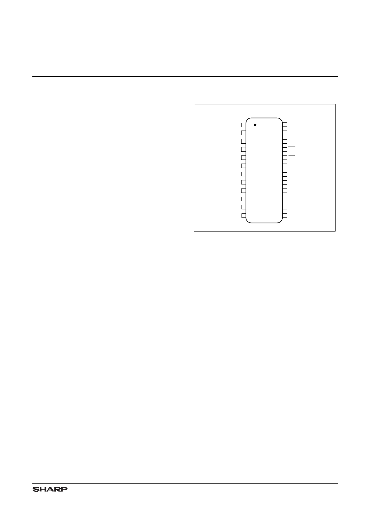
PIN CONNECTIONS
1
2
3
4
5
6
9
10
A
0
A
3
V
CC
24
23
22
21
20
19
16
15
A
5
A
4
7
8
A
1
A
2
18
17
A
7
A
6
OE
I/O
1
GND
A
8
A
9
A
10
CE
11
12
14
13
TOP VIEW
I/O
2
I/O
3
I/O
7
I/O
6
I/O
5
I/O
4
I/O
8
WE
5116S-1
24-PIN SOP
Figure 1. Pin Connections for SOP Package
1
Page 2
TRUTH TABLE
CE OE WE MODE I/O1 - I/O
8
SUPPLY CURRENT NOTE
L X L Write D
IN
Operating (ICC)1
L L H Read D
OUT
Operating (ICC)
H X X Deselect High-Z Standby (I
SB
)1
L H X Output disable High-Z Operating (I
CC
)1
NOTE:
1. X = H or L
I/O
8
A
8
A
9
A
10
23
22
19
9
13
16
5116S-2
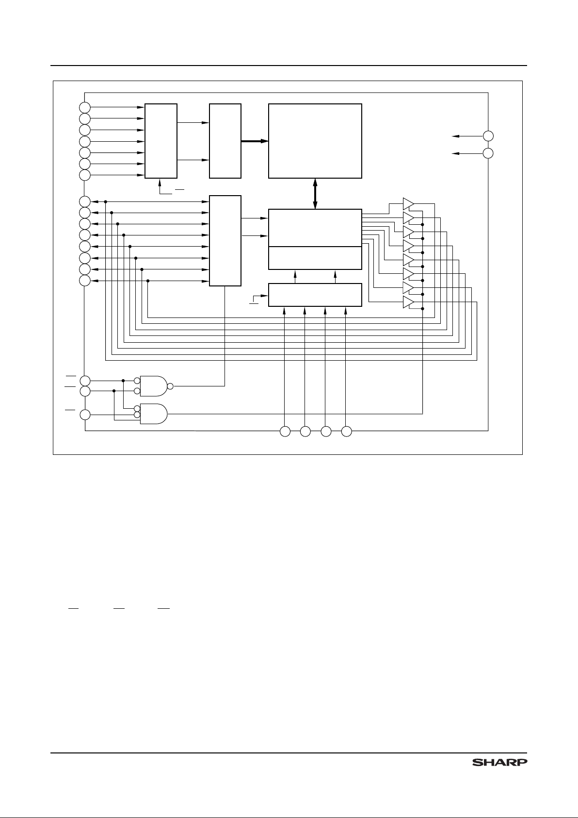
MEMORY CELL
ARRAY
(128 x128)
11
21
15
10
14
A
7
1
WE
ROW ADDRESS
BUFFERS
CE
A
6
2
A
5
3
18
A
0
8
ROW DECODERS
COLUMN
I/O CIRCUITS
COLUMN DECODERS
OE
DATA CONTROL
V
CC
GND
I/O
7
I/O
6
I/O
5
I/O
4
I/O
3
I/O
2
I/O
1
20
17
COLUMN ADDRESS
BUFFERS
4
A
4A3A2A1
7
5
6
24
12
CE
CE
Figure 2. LH5116S Block Diagram
PIN DESCRIPTI ON
SIGNA L PIN N AME
A0 - A
10
Addre ss input
CE Chip Ena ble in put
OE Outpu t E nab le inp ut
WE Wri te E na ble inp ut
SIGNAL PIN NAM E
I/O1 - I/O
8
Data i npu t/o utp ut
V
CC
Power sup ply
GND Ground
LH5116S CMOS 16K (2K × 8) Static RAM
2
Page 3
ABSOLUTE MAXIMUM RATINGS
PARAMETER SYMBOL RATING UNIT NOTE
Suppl y v olt age V
CC
-0.3 to +7.0 V 1
Input vol tage V
IN
-0.3 to VCC +0.3 V 1
Operating temperature Topr 0 to +50
°C
Storag e t emp era ture Tstg -55 to +150
°C
NOTE:
1. The maximum appl icable vol tage on any pin with respect to GND.
RECOMMENDED OPERATING CONDITIONS (TA = 0 to +50°C)
P A RAMETER SYMBOL MIN. TYP. MAX. UNIT
Suppl y v olt age V
CC
2.7 3.0 3.3 V
Input vol tage
V
IH
2.2 VCC + 0.3 V
V
IL
-0.3 0.8 V
DC CHARACTERISTICS (VCC = 3 V ± 10%, TA = 0 t o +50°C)
PARAMETER SYMBOL CONDITIONS MIN. TYP. MAX. UNIT NOTE
Output ‘L OW’ v olta ge V
OL
IOL = 2.1 mA 0.5 V
Output ‘H IGH ’ vol tage V
OH
IOH = -1.0 mA
V
CC
- 0.5 V
Input lea kag e c urr ent I
LI
VIN = 0 V to V
CC
-1.0 1.0
µA
Output le aka ge cur ren t I
LO
CE = VIH, V
I/O
= 0 V to V
CC
-1.0 1.0
µA
Operat ing cu rre nt
I
CC1
Outputs open (OE = VCC) 8 10 mA 1
I
CC2
Outputs open (OE = VIH) 8 10 mA 2
Standb y c urr ent I
CCL
CE ≥ VCC - 0.2 V
All other input pins = 0 V to V
CC
1.0
µA
NOTES:
1. C E = 0 V; all other input pins = 0 V to V
CC
2. CE = VIL; all other input pins = VIL to V
IH
AC CHARACTERISTICS (VCC = 3 V ± 10%, TA = 0 t o +50°C)
(1) READ CYCLE
PARAMETER SYMBOL MIN. TYP. MAX. UNIT NOTE
Read c yc le t ime t
RC
1000 ns
Addres s a cc ess ti me t
AA
1000 ns
Chip e nab le acc es s ti me t
ACE
1000 ns
Chip e nab le Low to ou tpu t in Lo w-Z t
CLZ
10 ns 1
Output en abl e a cce ss tim e t
OE
100 ns
Output en abl e L ow to o utp ut in Low -Z t
OLZ
10 ns 1
Chip d isa ble to ou tpu t i n Hi gh- Z t
CHZ
040ns1
Output en abl e t o ou tpu t i n H igh -Z t
OHZ
040ns1
Output ho ld time
t
OH
10 ns
NOTE:
1. Active out put to high-impedance and high-impedance to outp ut
active tests specified for a ±200 mV transition
from steady state levels into the test load.
CMOS 16K (2K × 8) Static RAM LH5116S
3
Page 4

(2) WRITE CYCLE (VCC = 3 V ± 10%, TA = 0 to +50°C)
PARAMETER SYMBOL MIN. T Y P. MAX. UNIT NOTE
Write c ycl e t ime t
WC
1000 ns
Chip e nab le to end of wri te t
CW
100 ns
Addres s v al id t ime t
AW
100 ns
Addres s s etu p t ime t
AS
0ns
Write p uls e w idt h t
WP
100 ns
Write re co ver y ti me t
WR
20 ns
WE Low to ou tpu t in Hi gh- Z t
WHZ
30 ns 1
Data v ali d t o e nd of w rit e t
DW
50 ns
Data h old ti me t
DH
20 ns
Output ac tiv e f rom end of wri te t
OW
10 ns 1
Output en abl e t o ou tpu t i n H igh -Z t
OHZ
040ns1
NOTE:
1. Active output to h igh-impedance and high-impedance to output
active tests specified for a ±200 mV transition
from steady state levels into the test load.
AC TEST CONDITIONS
PARAMETER MODE NOTE
Input voltage amplitude 0 to V
CC
Input rise/fall time 10 ns
Timing re fer enc e l eve l 1.5 V
Output lo ad con dit ion s C
L
(100 pF) 1
NOTE:
1. In cludes scope and jig capacitance.
DATA RETENTION CHARACTERISTICS (TA = 0 to +50°C)
PARAM ETER SYMBOL CONDITIONS MIN. TYP. MAX. UNIT NOTE
Data r ete nti on v ol tag e V
CCDR
CE ≥ V
CCDR
- 0.2 V
2.0 V
Data r ete nti on c urr ent
I
CCDR
CE ≥ V
CCDR
- 0.2 V,
V
CCDR
= 2.0 V
1.0
µA
0.2 1
Chip d isa ble to da ta rete nti on t
CDR
0ns
Recov ery tim e t
R
t
RC
ns 2
NOTES:
1.
T
A
= 25°C
2. t
RC
= Read cycle time
CAPACITANCE 1 (TA = 25° C, f = 1MHz)
PARAMETER SYMBOL CONDITIONS MIN. TYP. MAX. UNIT
Input cap acitan ce C
IN
VIN = 0 V 7 pF
Input/ out put ca pac ita nce C
I/O
VI/O = 0 V 10 pF
NOTE:
1. Th is parameter is sampled and not production tested.
LH5116S CMOS 16K (2K × 8) Static RAM
4
Page 5

2.5 V
DATA RETENTION MODE
V
CC
0 V
CE ≥ V
CCDR
-0.2 V
CE
2.2 V
t
CDR
5116S-6
t
R
V
CCDR
Figur e 3. Low Voltage Data Retention
t
OE
t
AA
A0 - A
10
CE
t
OLZ
t
OH
D
OUT
DATA VALID
t
OHZ
OE
t
RC
t
ACE
t
CHZ
t
CLZ
NOTE: WE = "HIGH"
5116S-3
Figure 4. Read Cycle
CMOS 16K (2K × 8) Static RAM LH5116S
5
Page 6

A0 - A
10
D
OUT
t
WC
t
AW
t
CW
t
WP
t
WHZ
t
OW
t
DH
t
DW
t
WR
(NOTE 3)
t
AS
(NOTE 2)
(NOTE 4)
5116S-4
WE
CE
D
IN
(NOTE 5)
(NOTE 6)
1. WE must be HIGH when there is a change in A0 - A10.
2. When CE and WE are both LOW at the same time, write occurs during the period t
WP
.
3. t
WR
is the time from the rise of CE or WE, whichever is first, to the end of the write cycle.
4. If CE LOW transition occurs at the same time or after WE LOW transition, the outputs will remain high-impedance.
5. D
OUT
outputs data with the same logic level as the input data of this write cycle.
6. If CE is LOW during this period, the input/output pins are in the output state. During this state, input
signals of opposite logic level must not be applied.
OE = 'LOW'
NOTES:
Figure 5. Wri te Cycle 1 (Note 1)
A0 - A
10
D
OUT
t
WC
t
AW
(NOTE 2)
WE
D
IN
t
CW
t
WP
t
OHZ
t
OW
t
WR
t
DH
t
DW
(NOTE 3)
t
AS
t
OLZ
OE
CE
(NOTE 5)
(NOTE 6)
(NOTE 4)
5116S-5
1. WE must be HIGH when there is a change in A0 - A10.
2. When CE and WE are both LOW at the same time, write occurs during the period t
WP
.
3. t
WR
is the time from the rise of CE or WE, whichever is first, to the end of the write cycle.
4. If CE LOW transition occurs at the same time or after WE LOW transition, the outputs will remain high-impedance.
5. D
OUT
outputs data with the same logic level as the input data of this write cycle.
6. If CE and OE are LOW during this period, the input/output pins are in the output state. During this state, input
signals of opposite logic level must not be applied.
NOTES:
Figure 6. Write Cycle 2 (Note 1)
LH5116S CMOS 16K (2K × 8) Static RAM
6
Page 7

24-pin, 450-mil SOP (SOP024-P-0450B)
LH5116S
Device Type
5116S-7
Example: LH5116SN (CMOS 16K (2K x 8) Static RAM, 450-mil SOP)
CMOS 16K (2K x 8) Static RAM
N
Package
ORDERING INFORMATION
DIMENSIONS IN MM [INCHES]
MAXIMUM LIMIT
MINIMUM LIMIT
24SOP (SOP024-P-0450B)
12.40 [0.488]
11.60 [0.457]
8.80 [0.346]
8.40 [0.331]
10.60 [0.417]
15.60 [0.614]
15.20 [0.598]
0.15 [0.006]
1.025 [0.040]
0.20 [0.008]
0.00 [0.000]
1.025 [0.040]
2.40 [0.094]
2.00 [0.079]
0.20 [0.008]
0.10 [0.004]
0.50 [0.120]
0.30 [0.012]
1.27 [0.050]
TYP.
24 13
121
1.70 [0.067]
1.70 [0.067]
24SOP
24-pin, 450-mil SOP
PACKAGE DIAGRAM
CMOS 16K (2K × 8) Static RAM LH5116S
7
 Loading...