

Page 1

®
PRODUCT SPECIFICATIONS
Integrated Circuits Group
LH28F800BVB-TTL90
Flash Memory
8M (1M × 8/512K × 16)
(Model No.: LHF80V07)
Spec No.: EL114067
Issue Date: August 27, 1999
Page 2
SHARP
LHFSOVO7
@Handle this document carefully for it contains material protected by international copyright law.
Any reproduction, full or in part, of this material is prohibited without the express written
permission of the company.
l When using the products covered herein, please observe the conditions written herein and the
precautions outlined in the following paragraphs. In no event shall the company be liable for any
damages resulting from failure to strictly adhere to these conditions and precautions.
(1) The products covered herein are designed and manufactured for the following application
areas. When using the products covered herein for the equipment listed in Paragraph (2),
even for the following application areas, be sure to observe the precautions given in
Paragraph (2). Never use the products for the equipment listed in Paragraph (3).
*Office electronics
*Instrumentation and measuring equipment
*Machine tools
*Audiovisual equipment
*Home appliance
*Communication equipment other than for trunk lines
(2) Those contemplating using the products covered herein for the following equipment which
demands high reliabilitv, should first contact a sales representative of the company and then
accept responsibility for incorporating into the design fail-safe operation, redundancy, and
other appropriate measures for ensuring reliability and safety of the equipment and the
overall system.
*Control and safety devices for airplanes, trains, automobiles, and other
transportation equipment
*Mainframe computers
*Traffic control systems
l Gas leak detectors and automatic cutoff devices
*Rescue and security equipment
*Other safety devices and safety equipment, etc.
(3) Do not use the products covered herein for the following equipment which demands
extremely high performance in terms of functionality, reliability, or accuracy.
*Aerospace equipment
l Communications equipment for trunk lines
*Control equipment for the nuclear power industry
l Medical equipment related to life support, etc.
(4) Please direct all queries and comments regarding the interpretation of the above three
Paragraphs to a sales representative of the company.
@Please direct all queries regarding the products covered herein to a sales representative of the
company.
Rev. 1.1
Page 3
SliARP
LHF80V07
CONTENTS
PAGE
1 INTRODUCTION.. ...........................................................
1. I Features ........................................................................
1.2 Product Overview.. ......................................................
2 PRINCIPLES
2.1 Data Protection..
3 BUS OPERATION ...........................................................
3.1 Read.. ...........................................................................
3.2 Output Disable..
3.3 Standby
3.4 Deep Power-Down..
3.5 Read Identifier Codes Operation..
3.6 Write..
4 COMMAND
4.1 Read Array Command ................................................
4.2 Read Identifier Codes Command
4.3 Read Status Register Command..
4.4 Clear Status Register Command ................................. 12
4.5 Block Erase Command..
4.6 Word/Byte Write Command..
4.7 Block Erase Suspend Command
4.8 Word/Byte Write Suspend Command..
4.9 Considerations of Suspend.. ....................................... 14
4.10 Block Locking.. ........................................................ 14
4.10.1 V,,=V,, for Complete Protection..
4.10.2 WP#=V,, for Block Locking.. ............................
4.10.3 WP#=V,, for Block Unlocking.. ........................ 14
OF OPERATION..
...........................................................
...........................................................
......................................................................... 8
..................................................... 8
.............................................
DEFINITIONS..
.....................................
...............................
. ............................
................
.............................................
.: .........................
............................... 12
............................... 12
..................................... 13
................................ 13
...................... 14
....................
.3
3
.3
.7
8
.8
.8
.8
.9
.9
9
12
12
14
14
PAGE
5 DESIGN CONSIDERATIONS
5.1 Three-Line Output Control .......................................
5.2 RY/BY# and Block Erase and Word/Byte Write
Polling.. .................................................................... 20
5.3 Power Supply Decoupling ........................................
5.4 V,, Trace on Printed Circuit Boards ........................ 20
5.5 V,, . V,,, RP# Transitions.. ..................................... 21
5.6 Power-Up/Down Protection..
5.7 Power Dissipation..
6 ELECTRICAL SPECIFICATIONS ............................... 22
6.1 Absolute Maximum Ratings ..................................... 22
6.2 Operating Conditions
6.2.1 Capacitance.. ....................................................... 22
6.2.2 AC Input/Output Test Conditions
6.2.3 DC Characteristics ..............................................
6.2.4 AC Characteristics - Read-Only Operations.. ..... 26
6.2.5 AC Characteristics - Write Operations
6.2.6 Alternative CE#-Controlled Writes..
6.2.7 Reset Operations .................................................
6.2.8 Block Erase and Word/Byte Write Performance 34
7 PACKAGE AND PACKING SPECIFICATIONS ......... 35
................................................... 21
...................................... 20
20
20
....................................
................................................
....................... 23
............... 29
...................
2 1
22
24
3 1
33
1
Rev. 1.1
Page 4
SHARIP
LH28F8OOBVB-TTL90
8M-BIT (1Mbit x 8 / 5 12Kbit x 16)
Smart3 Flash MEMORY
n Smart3 Technology
- 2.7V-3.6V Vcc
-
2.7V-3.6V or 11.4V-12.6V Vpp
n User-Configurable x8 or x 16 Operation
n High-Performance Access Time
- 90ns(2.7V-3.6V)
n Operating Temperature
- 0°C to +7O”C
n Optimized Array Blocking Architecture
-
Two 4K-word Boot Blocks
-
Six 4K-word Parameter Blocks
-
Fifteen 32K-word Main Blocks
-
Top Boot Location
n Extended Cycling Capability
-
100,000 Block Erase Cycles
n Enhanced Automated Suspend Options
-
Word/Byte Write Suspend to Read
-
Block Erase Suspend to Word/Byte Write
-
Block Erase Suspend to Read
LHF80V07
n Enhanced Data Protection Features
n Automated Word/Byte Write and Block Erase
n Low Power Management
n SRAM-Compatible Write Interface
n Chip Size Packaging
n ETOXTM* Nonvolatile Flash Technology
n CMOS Process (P-type silicon substrate)
n Not designed or rated as radiation hardened
-
Absolute Protection with Vpp=GND
-
Block Erase and Word/Byte Write Lockout
during Power Transitions
-
Boot Blocks Protection with WP#=VIL
-
Command User Interface
- Status Register
-
Deep Power-Down Mode
-
Automatic Power Savings Mode Decreases
ICC in Static Mode
- 48-Ball CSP
2
SHARP’s LH28F800BVB-TTL90 Flash memory with Smart3 technology is a high-density, low-cost, nonvolatile, read/write
storage solution for a wide range of applications. LH28F800BVB-TTL90 can operate at V,,=2.7V-3.6V and V,,=2.7V-3.6V
Its low voltage operation capability realize battery life and suits for cellular phone application.
Its Boot. Parameter and Main-blocked architecture, flexible voltage and extended cycling provide for highly flexible
:omponent suitable for portable terminals and personal computers. Its enhanced suspend capabilities provide for an ideal
solution for code + data storage applications. For secure code storage applications, such as networking, where code is either
lirectly executed out of flash or downloaded to DRAM, the LH28F8OOBVB-TTL90 offers two levels of protection: absolute
lrotection with V,, at GND, selective hardware boot block locking. These alternatives give designers ultimate control of their
:ode security needs.
Ihe LH28F800BVB-TTL90 is manufactured on SHARP’s 0.35um ETOXTM* process technology. It come in chip-size
lackage: the 48-ball CSP ideal for board constrained applications.
“ETOX is a trademark of Intel Corporation
Rev. 1.1
Page 5
SHARP
LHF8OVO7 3
1 INTRODUCTION
This datasheet contains LH28F800BVB-TI’L90
specifications. Section 1 provides a flash memory
overview. Sections 2,3,4 and 5 describe the memory
organization and functionality. Section 6 covers electrical
specifications.
1.1 Features
Key enhancements of LH28F8OOBVB-TTL90 Smart3
Flash memory are:
*Smart3 Technology
*Enhanced Suspend Capabilities
*Boot Block Architecture
Please note following important differences:
l
VPPLK has been lowered to 1.5V to support 2.7V-3.6V
block erase and word/byte write operations. The V,,
voltage transitions to GND is recommended for
designs that switch V,, off during read operation.
*To take advantage of Smart3 technology, allow V,,
and V,, connection to 2.7V-3.6V.
1.2 Product Overview
The LH28F800BVB-TTL90 is a high-performance 8M-bit
Smart3 Flash memory organized as lM-byte of 8 bits or
512K-word of 16 bits. The lM-byte/512K-word of data is
uranged in two 8K-byte/4K-word boot blocks, six SKJytel4K-word parameter blocks and fifteen 64K-byte/32Kword main blocks which are individually erasable intystem. The memory map is shown in Figure 3.
Smart3 technology provides a choice of V,, and V,,
:ombinations, as shown in Table 1, to meet system
xrformance and power expectations. V,, at 2.7V-3.6V
:liminates the need for a separate 12V converter, while
V,,=12V maximizes block erase and word/byte write
performance. In addition to flexible erase and program
voltages. the dedicated V,, pin gives complete data
protection when VPplVPPLK.
Table 1. V,, and V,, Voltage Combinations Offered by
Smart3 Technoloav
V,, Voitage
i
2.7V-3.6V 1 2.7V-3.6V, 11.4V-12.6V 1
Internal V,, and V,, detection Circuitry automatically
configures the device for optimized read and write
operations.
A Command User Interface (CUI) serves as the interface
between the system processor and internal operation of the
device. A valid command sequence written to the CUI
initiates device automation. An internal Write State
Machine (WSM) automatically executes the algorithms
and timings necessary for block erase and word/byte write
operations.
A block erase operation erases one of the device’s 32Kword blocks typically within 0.51s (2.7V-3.6V V,,,
11.4V-12.6V V,,), 4K-word blocks typically within 0.3 1s
(2.7V-3.6V V,,, 11.4V-12.6V V,,) independent of other
blocks. Each block can be independently erased 100,000
times. Block erase suspend mode allows system software
to suspend block erase to read or write data from any other
block.
Writing memory data is performed in word/byte
increments of the device’s 32K-word blocks typically
within 12.6~~ (2.7V-3.6V V,,, 11.4V-12.6V V,,), 4Kword blocks typically within 24.5~~ (2.7V-3.6V V,,,
11.4V-12.6V V,,). Word/byte write suspend mode
enables the system to read data or execute code from any
other flash memory array location.
LzJ
V,, Voltage
Rev. 1.1
Page 6
SHARP
LHF8OVO7 4
The boot blocks can be locked for the WP# pin. Block
erase or word/byte write for boot block must not be carried
out by WP# to Low and RP# to V,,.
The status register indicates when the WSM’s block erase
or word/byte write operation is finished.
The RY/BY# output gives an additional indicator of WSM
activity by providing both a hardware signal of status
(versus software polling) and status masking (interrupt
masking for background block erase, for example). Status
polling using RY/BY# minimizes both CPU overhead and
system power consumption. When low, RY/BY# indicates
that the WSM is performing a block erase or word/byte
write. RY/BY#-high Z indicates that the WSM is ready for
a new command, block erase is suspended (and word/byte
write is inactive), word/byte write is suspended, or the
device is in deep power-down mode.
The access time is 90ns (tAv
temperature range (O’C to +70 43
range of 2.7V-3.6V.
v) over the commercial
) and V,, supply voltage
The Automatic Power Savings (APS) feature substar&&
reduces active current when the device is in static modf
(addresses not switching). In APS mode, the typical I,,
current is 3 mA at 2.7V V,,.
When CE# and RP# pins are at V,-,, the I,, CM05
standby mode is enabled. When the RP# pin is at GND
deep power-down mode is enabled which minimize:
power consumption and provides write protection during
reset. A reset time (tpHQv)
high until outputs are valid. Likewise, the device has i
wake time (tpHEL ) from RP#-high until writes to the CUI
are recognized. With RP# at GND, the WSM is reset ant
the status register is cleared.
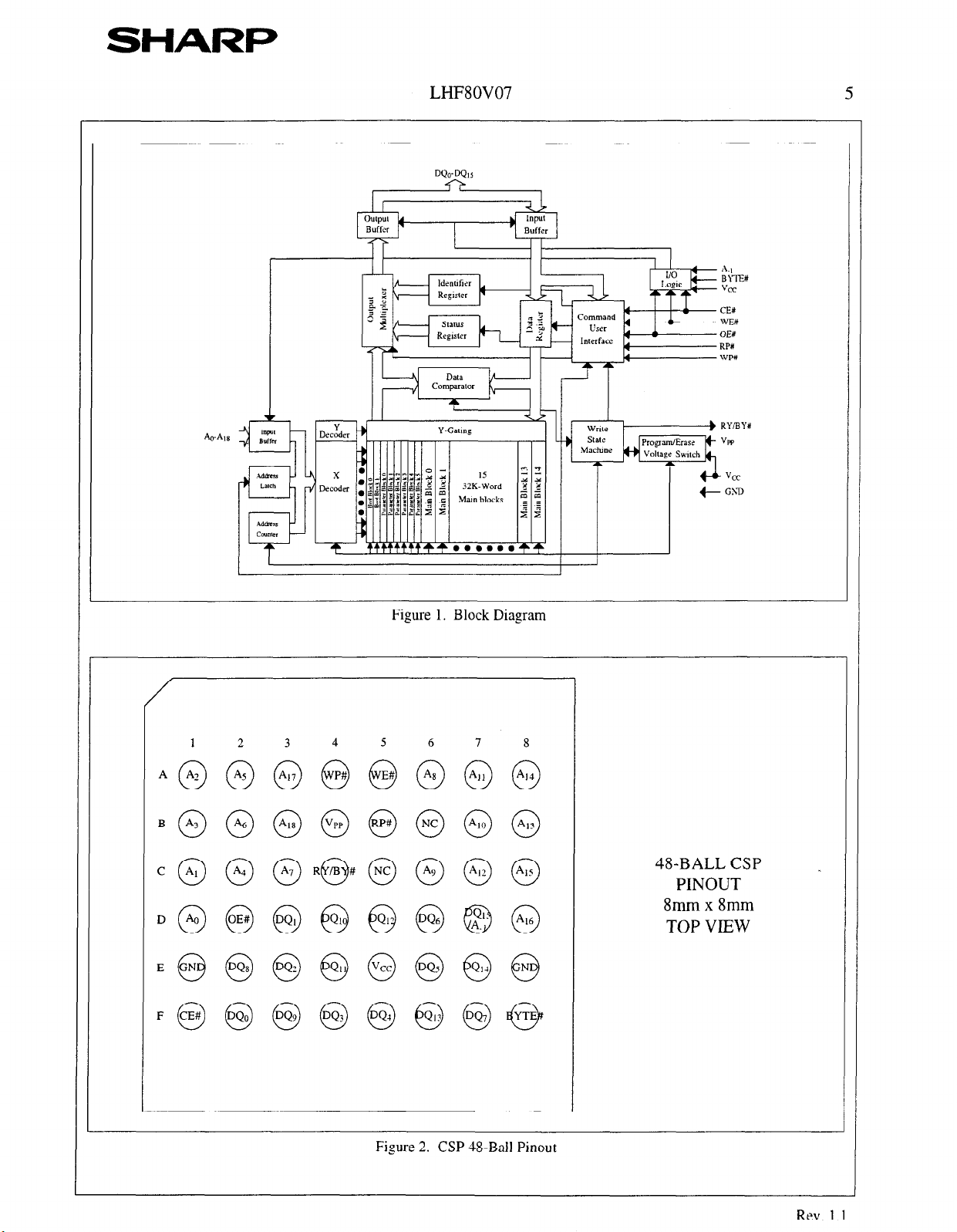
The device is available in 48-ball CSP (Chip Size
Package). Pinout is shown in Figure 2.
is required from RP# switching
Rev. 1.1
Page 7
SHARP
LHF8OVO7 5
DUO-DQls
r
1
A 0 A?
B
0
A3
C
0 Al
D 0 Ao
F 0 CE#
2
A5
0
%
0
A4
0
OE#
0
DQ8
0
DQo
0
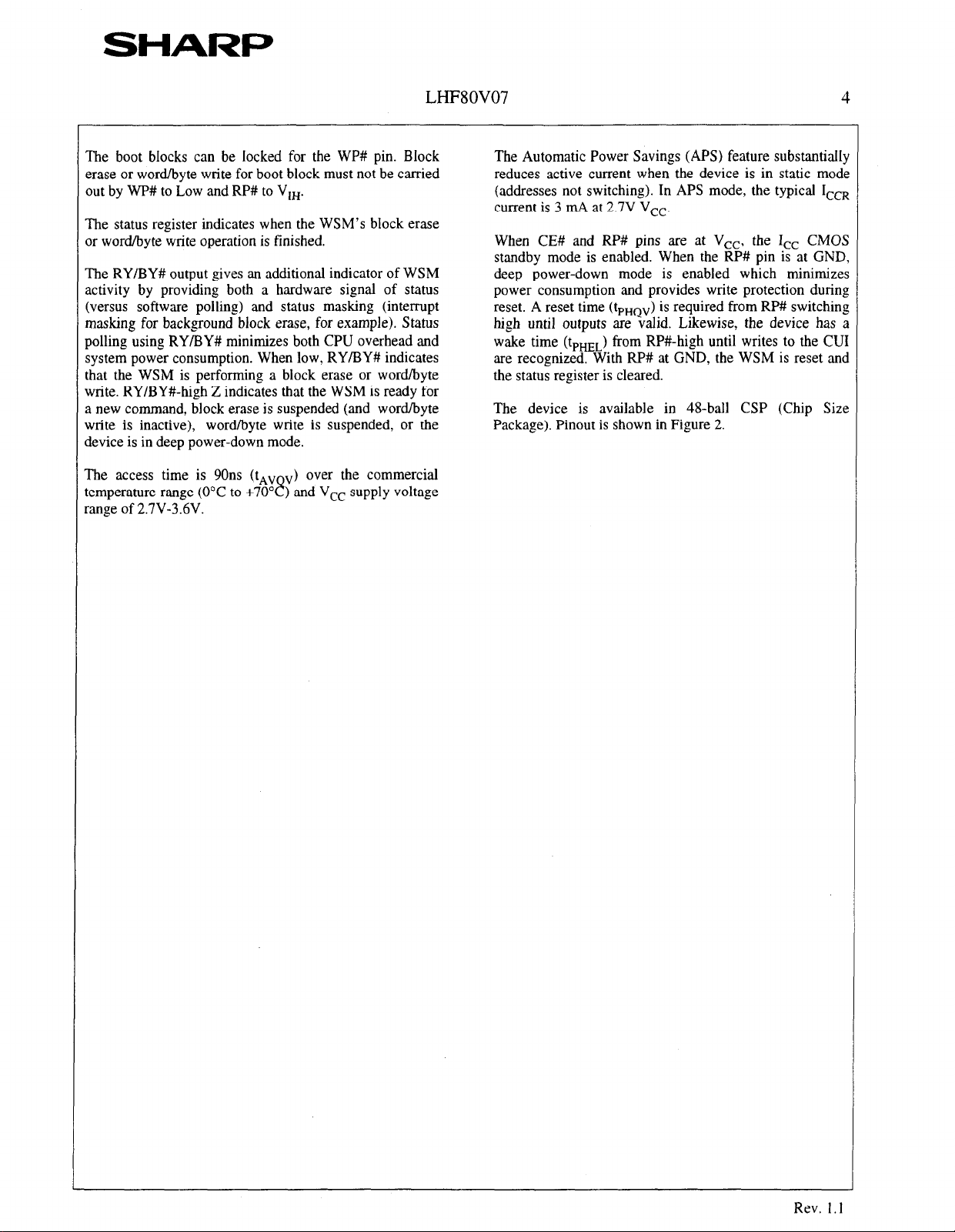
Figure 1. Block Diagram
6
A8
0
NC
0
A9
0
DQ6
0
DQ5
0
Ql?
0
7
All
0
AIO
0
Al?
0
0
DQ7
0
QM
.%‘I
0
AI?
0
Al5
0
A16
0
8
4%BALL CSP
PINOUT
8mm x 8mm
TOP VIEW
Figure 2. CSP #-Ball Pinout
Rev. 1.1
Page 8
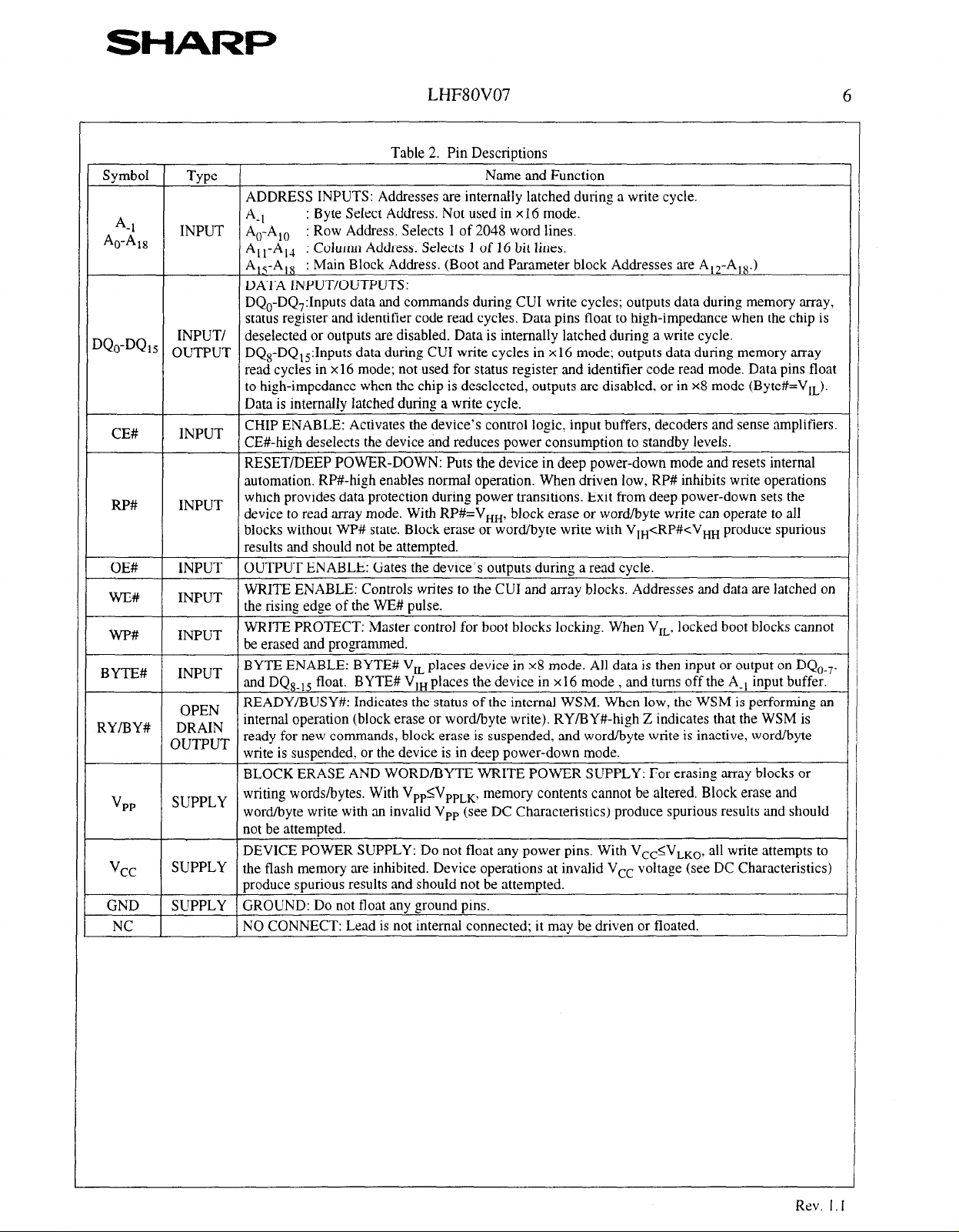
SHARP
r
Symbol
A-,
Ao-Al8
1
DQo-DQ,,
CE#
RP#
OE#
WE# INPUT
WP# INPUT
BYTE# INPUT
RY/BY#
VCC
NC
Type
INPUT
INPUT/
OUTPUT
INPUT
INPUT
INPUT
OPEN
DRAIN
DUTPUT
SUPPLY
SUPPLY
SUPPLY GND
LHF8OVO7
Table 2. Pin Descriptions
Name and Function
ADDRESS INPUTS: Addresses are internally latched during a write cycle.
A-1
Ao-Alo
All-*,, .
<
DATA INPUT/OUTPUTS:
DQo-DQ-/:Inputs data and commands during CUI write cycles; outputs data during memory array,
status
deselected or outputs are disabled. Data is internally latched during a write cycle.
DQs-DQ, j:Inputs data during CUI write cycles in xl6 mode; outputs data during memory array
read cycles in x 16 mode; not used for status register and identifier code read mode. Data pins float
to high-impedance when the chip is deselected, outputs are disabled. or in x8 mode (Byte#=V,,J
Data is intemallv latched during a write cvcle.
CHIP ENABLE: Activates the device’s control logic. input buffers, decoders and sense amplifiers.
CE#-high deselects the device and reduces power consumption to standby levels.
RESET/DEEP POWER-DOWN: Puts the device in deep power-down mode and resets internal
automation. RP#-high enables normal operation. When driven low, RP# inhibits write operations
which provides data protection during power transitions. Exit from deep power-down sets the
device to read array mode. With RP#=V,,, block erase or word/byte write can operate to all
blocks without WP# state. Block erase or word/byte write with Vt,<RP#<V,B produce spurious
results and should not be attempted.
OUTPUT ENABLE: Gates the device’s outputs during a read cycle.
WRITE ENABLE: Controls writes to the CUI and atray blocks. Addresses and data are latched on
the rising edge of the WE# uulse.
WRITE PROTECT: Master control for boot blocks locking. When V,. locked boot blocks cannot
be erased and Droerammed.
BYTE ENABLE: BYTES V,, places device in x8 mode. All data is then input or output on DQ,,.
and DQ8-t5 float. BYTE# V,, places the device in x16 mode , and turns off the A-, input buffer.
READY/BUSY#: Indicates the status of the internal WSM. When low, the WSM is performing an
internal operation (block erase or word/byte write). RY/BY#-high Z indicates that the WSM is
ready for new commands, block erase is suspended. and word/byte write is inactive, word/byte
write is suspended, or the device is in deep power-down mode.
BLOCK ERASE AND WORD/BYTE WRITE POWER SUPPLY: For erasing array blocks or
writing words/bytes. With V,,IV,,,,. memory contents cannot be altered. Block erase and
word/byte write with an invalid V,, (see DC Characteristics) produce spurious results and should
not be attempted.
DEVICE POWER SUPPLY: Do not float any power pins. With V&V,,,, all write attempts to
the flash memory are inhibited. Device operations at invalid V,, voltage (see DC Characteristics)
oroduce sourious results and should not be attemuted.
GROUND: Do not float any ground pins.
NO CONNECT: Lead is not internal connected; it may be driven or floated.
: Byte Select Address. Not used in x16 mode.
: Row Address. Selects 1 of 2048 word lines.
. Column Address. Selects 1 of 16 bit lines.
register and identifier code read cycles. Data pins float to high-impedance when the chip is
6
Rev. I.1
i
Page 9
SHARP
LHF80V07 7
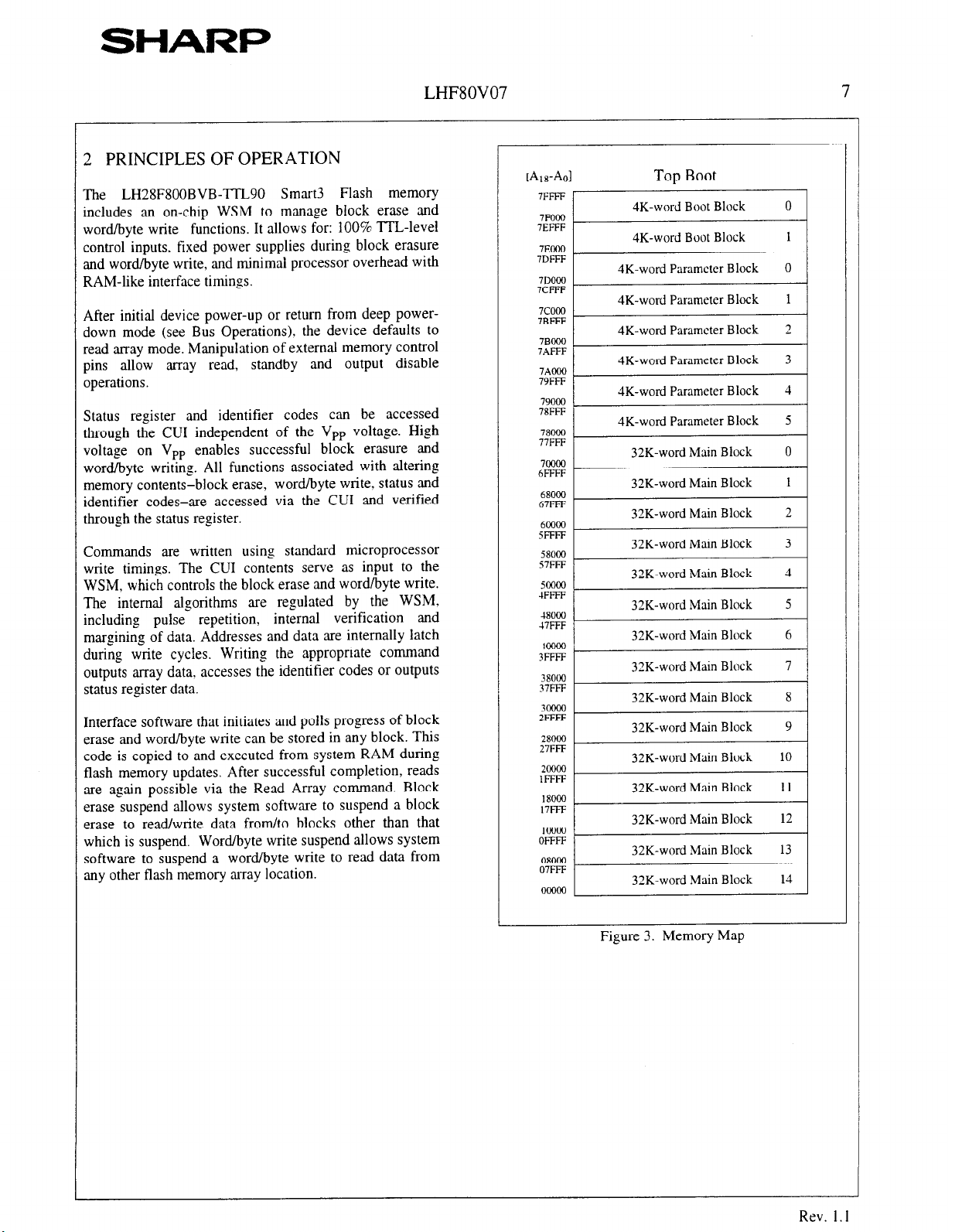
2 PRINCIPLES OF OPERATION
The LH28F800BVB-TTL90 Smart3 Flash memory
includes an on-chip WSM to manage block erase and
word/byte write functions. It allows for: 100% TTL-level
control inputs. fixed power supplies during block erasure
and word/byte write, and minimal processor overhead with
RAM-like interface timings.
After initial device power-up or return from deep powerdown mode (see Bus Operations). the device defaults to
read array mode. Manipulation of external memory control
pins allow array read, standby and output disable
operations.
Status register and identifier codes can be accessed
through the CUI independent of the V,, voltage. High
voltage on VP, enables successful block erasure and
word/byte writing. All functions associated with altering
memory contents-block erase, word/byte write, status and
identifier codes-are accessed via the CUI and verified
through the status register.
Commands are written using standard microprocessor
write timings. The CUI contents serve as input to the
WSM, which controls the block erase and word/byte write.
The internal algorithms are regulated by the WSM.
including pulse repetition, internal verification and
margining of data. Addresses and data are internally latch
during write cycles. Writing the appropriate command
outputs array data. accesses the identifier codes or outputs
status register data.
Interface software that initiates and polls progress of block
erase and word/byte write can be stored in any block. This
code is copied to and executed from system RAM during
flash memory updates. After successful completion, reads
Ire again possible via the Read Array command. Block
:rase suspend allows system software to suspend a block
erase to read/write data from/to blocks other than that
which is suspend. Word/byte write suspend allows system
;oftware to suspend a word/byte write to read data from
ury other flash memory array location.
r
tA18-&1 Top Boot
7FFFF
7FOO0
7EFFF
7EOOO
7DFFF
7DOOil
7CFFF
7coOO
7BFFF
7BOOQ
7AFFF
7.&m
79FFF
79000
78FFF
78OOa
77FFF
7oOw
6FFFF
68000
67FFF
60000
5FFFF
58000
57FFF
50000
4FFFF
48000
47FFF
-1oooo
3FFFF
38000
37FFF
3moo
ZFFFF
28000
27FFF
20000
IFFFF
18000 I
17FFF
1OQOO
OFFFF
08000
07FFF
00000
4K-word Boot Block 0
4K-word Boot Block 1
4K-word Parameter Block
4K-word Parameter Block 1
4K-word Parameter Block
4K-word Parameter Block 3
4K-word Parameter Block 4
4K-word Parameter Block
32K-word Main Block 0
32K-word Main Block
32K-word Main Block 2
32K-word Main Block 3
32K-word Main Block 4
32K-word Main Block 5
32K-word Main Block 6
32K-word Main Block
32K-word Main Block 8
32K-word Main Block 9
32K-word Main Block
32K-word Main Block 11
32K-word Main Block 12
32K-word Main Block 13
32K-word Main Block 14
1
0
2
5
1
7
10
Figure 3. Memory Map
Rev. 1.1
Page 10
SHARI=
LHF8OVO7
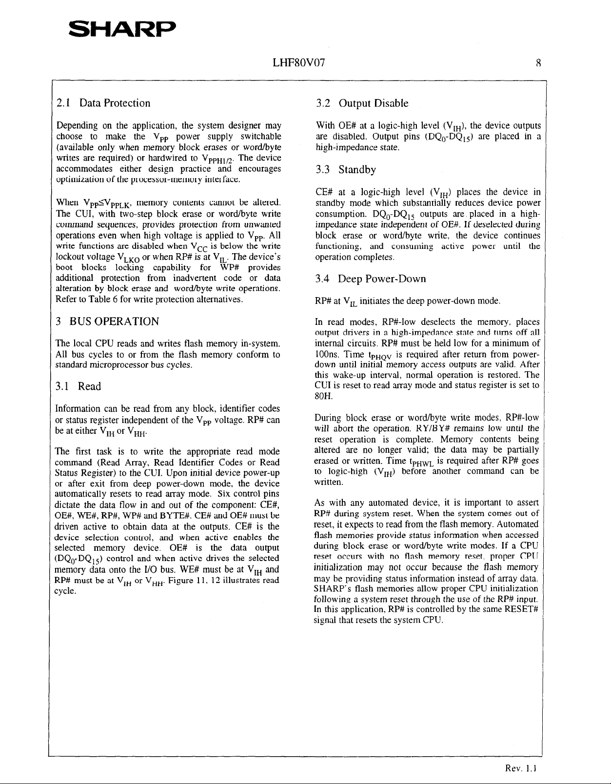
2.1 Data Protection
Depending on the application, the system designer may
choose to make the V,, power supply switchable
(available only when memory block erases or word/byte
writes are required) or hardwired to VPPHIR. The device
accommodates either design practice and encourages
optimization of the processor-memory interface.
When VPPIVPPLK.
The CUI, with two-step block erase or word/byte write
command sequences, provides protection from unwanted
operations even when high voltage is applied to V,,. All
write functions are disabled when V,, is below the write
lockout voltage V,,, or when RP# is at V,,. The device’s
boot blocks locking capability for WP# provides
additional protection from inadvertent code or data
alteration by block erase and word/byte write operations.
Refer to Table 6 for write protection alternatives.
memory contents cannot be altered.
3 BUS OPERATION
The local CPU reads and writes flash memory in-system.
All bus cycles to or from the flash memory conform to
standard microprocessor bus cycles.
3.1 Read
[nformation can be read from any block, identifier codes
Jr status register independent of the V,, voltage. RP# can
5e at either V,, or V,,.
The first task is to write the appropriate read mode
:ommand (Read Array, Read Identifier Codes or Read
Status Register) to the CUI. Upon initial device power-up
x after exit from deep power-down mode. the device
automatically resets to read array mode. Six control pins
dictate the data flow in and out of the component: CE#,
3E#, WE#, RP#, WP# and BYTE#. CE# and OE# must be
Iriven active to obtain data at the outputs. CE# is the
device selection control, and when active enables the
;elected memory device. OE# is the data output
DQorDQlj) control and when active drives the selected
nemory data onto the I/O bus. WE# must be at V,, and
iP# must be at V,, or V,,. L Figure 11 12 illustrates read ,
:ycle.
3.2 Output Disable
With OE# at a logic-high level (V,,), the device outputs
are disabled. Output pins (DQ,-DQ,,) are placed in a
high-impedance state.
3.3 Standby
CE# at a logic-high level (VrH) places the device in
standby mode which substantially reduces device power
consumption. DQO-DQ,, outputs are placed in a highimpedance state independent of OE#. If deselected during
block erase or word/byte write. the device continues
functioning, and consuming active power until the
operation completes.
3.4 Deep Power-Down
RP# at V, initiates the deep power-down mode.
In read modes, RP#-low deselects the memory. places
output drivers in a high-impedance state and turns off all
internal circuits. RP# must be held low for a minimum of
loons. Time tpHQV
down until initial memory access outputs are valid. After
this wake-up interval, normal operation is restored. The
CUI is reset to read array mode and status register is set to
80H.
During block erase or word/byte write modes? RP#-low
will abort the operation. RY/BY# remains low until the
reset operation is complete. Memory contents being
altered are no longer valid; the data may be partially
erased or written. Time tpHwL is required after RP# goes
to logic-high (V,,) before another command can be
written.
As with any automated device, it is important to assert
RP# during system reset. When the system comes out of
reset, it expects to read from the flash memory. Automated
flash memories provide status information when accessed
during block erase or word/byte write modes. If a CPU
reset occurs with no flash memory reset. proper CPU
initialization may not occur because the flash memory
may be providing status information instead of array data.
SHARP’s flash memories allow proper CPU initialization
following a system reset through the use of the RP# input.
In this application, RP# is controlled by the same RESET#
signal that resets the system CPU.
is required after return from power-
Rev. 1.1
Page 11
SHARP
LHF8OVO7 9
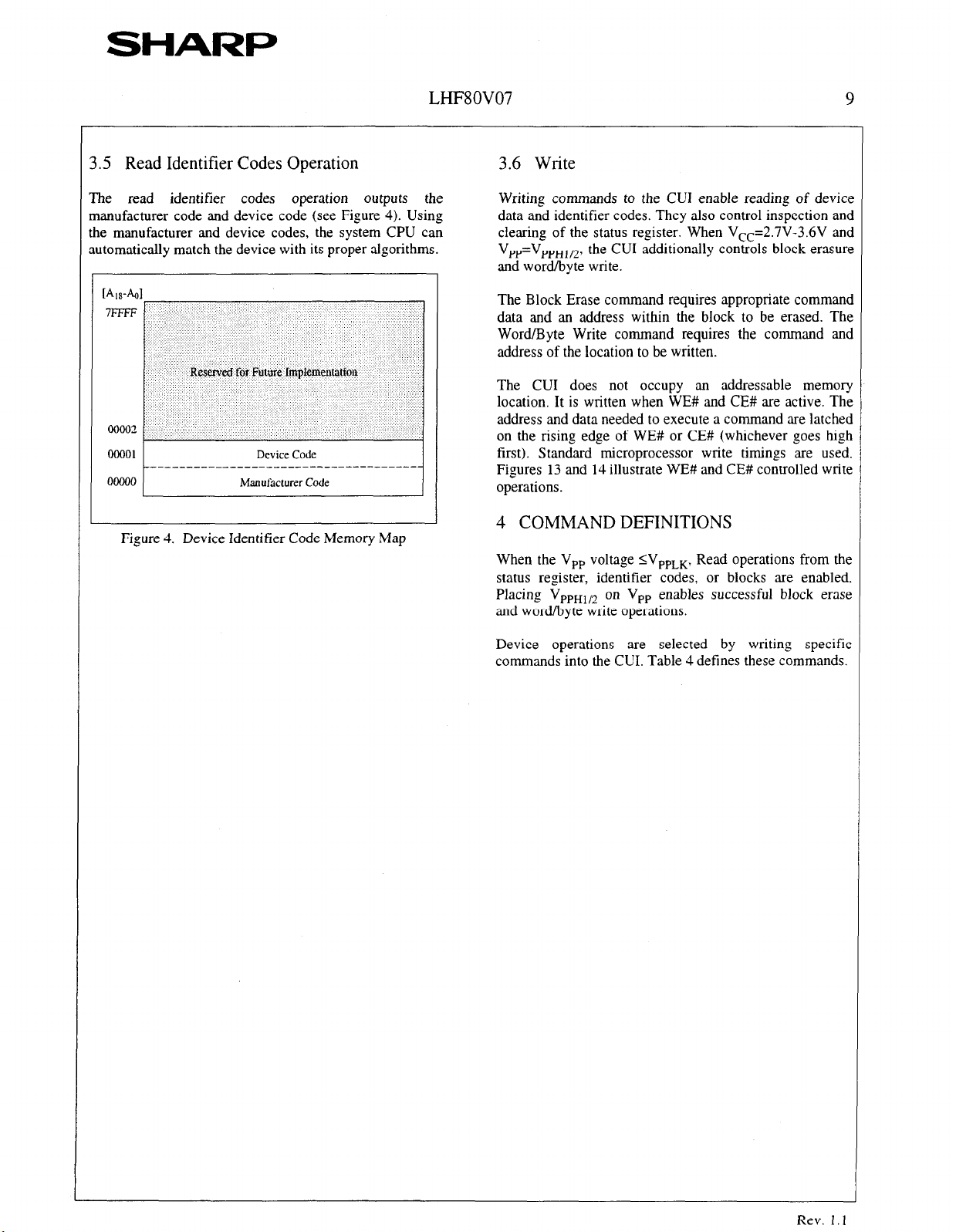
.5 Read Identifier Codes Operation 3.6 Write
he read identifier codes operation
manufacturer code and device code (see Figure 4). Using
le manufacturer and device codes, the system CPU can
ltomatically match the device with its proper algorithms.
Device Code
Manufacturer Code
Figure 4. Device Identifier Code Memory Map
outputs
the
Writing commands to the CUI enable reading of device
data and identifier codes. They also control inspection ant
clearing of the status register. When V,-=2.7V-3.6V ant
VPt,=VPPH1,2, the CUI additionally controls block erasure
and word/byte write.
The Block Erase command requires appropriate commanc
data and an address within the block to be erased. The
Word/Byte Write command requires the command and
address of the location to be written.
The CUI does not occupy an addressable memory
location. It is written when WE# and CE# are active. The
address and data needed to execute a command are latched
on the rising edge of WE# or CE# (whichever goes high
first). Standard microprocessor write timings are used.
Figures 13 and 14 illustrate WE# and CE# controlled write
operations.
4 COMMAND DEFINITIONS
When the V,, voltage IV,,,,. Read operations from the
status register, identifier codes, or blocks are enabled.
Placing VP,,,,* on V,, enables successful block erase
and word/byte write operations.
Device operations are selected by writing specific
commands into the CUI. Table 4 defines these commands.
Rev. 1.1
Page 12

SHARI=
LHF8OV07
Table 3.1. Bus Operations(BYTE#=Vu.,)(l,z)
Mode
Read
Output Disable
Standby
Deep Power-Down
Read Identifier Codes
Write
Notes RP# CE# OE# WE# Address V,,
8
10
4,lO
8
6,7,8
‘I, Or
VU,
‘1, Or
‘HH
‘1, Or
vnH
VI,
‘1, Or
vIiH
VIEI Or
‘HH
VI, VI, ‘1,
VI, VI,
‘1,
X X X
‘1,
X X
VI, VI, ‘1,
VI, vIH VI,
X
X
X X
See
Figure 4
X X
X
X High Z X
X High Z X
X High Z High Z
X
Table 3.2. Bus Operations(BYTE#=VIL)(1,2)
Mode
Read
Output Disable
Standby
Deep Power-Down
Read Identifier Codes
Write
Notes
8
10
4,lO
8.9
fj 7 8
> >
RP# CE# OE#
vIH Or
VHH
vIH Or
VHH
‘1, Or
vHH
VI,
vIH Or
‘HH
VIHor
vHH
VI, VI, ‘1,
VIL ‘1, ‘IH
‘1,
X X X X
VI, VI, ‘1,
VIL ‘1, VIL
WE# Address
X X
VW
X
X X HighZ HighZ X
X
See
Figure 4
X X
DQ,, DQ,-,, RY/BY#(3)-
X
Dour
X High Z High Z X
X High Z High Z High Z
X Note 5 High Z High Z
NOTES:
1. Refer to DC Characteristics. When V,,5V,,,,,
2. X can be VI, or VI, for control pins and addresses, and V,, or VPPHIjz
memory contents can be read, but not altered.
for V,,. See DC Characteristics for V,,, and
V,,,,,, voltages.
3. RY/BY# is V,, when the WSM is executing internal block erase or word/byte write algorithms, It is High Z during when
the WSM is not busy, in block erase suspend mode (with word/byte write inactive), word/byte write suspend mode or
deep power-down mode.
4. RP# at GNDk0.2V ensures the lowest deep power-down current.
5. See Section 4.2 for read identifier code data.
6. Command writes involving block erase or word/byte write are reliably executed when VPP=VPPH1/2 and V,,=2.7V-3.6V.
Block erase or word/byte write with Vm<RP#<VHH produce spurious results and should not be attempted.
7. Refer to Table 4 for valid DIN during a write operation.
8. Never hold OE# low and WE# low at the same timing.
9. A-, set to VI, or VI, in byte mode (BYTE#=V,,).
lo. m# set to vIL or VI,.
DQ,,,5 RY/BY#c3)
DOUT
Note 5 High Z
DIN
High Z X
DIN
X X
X
X
Rev. 1.1
Page 13
SHARP
LHF80V07 11
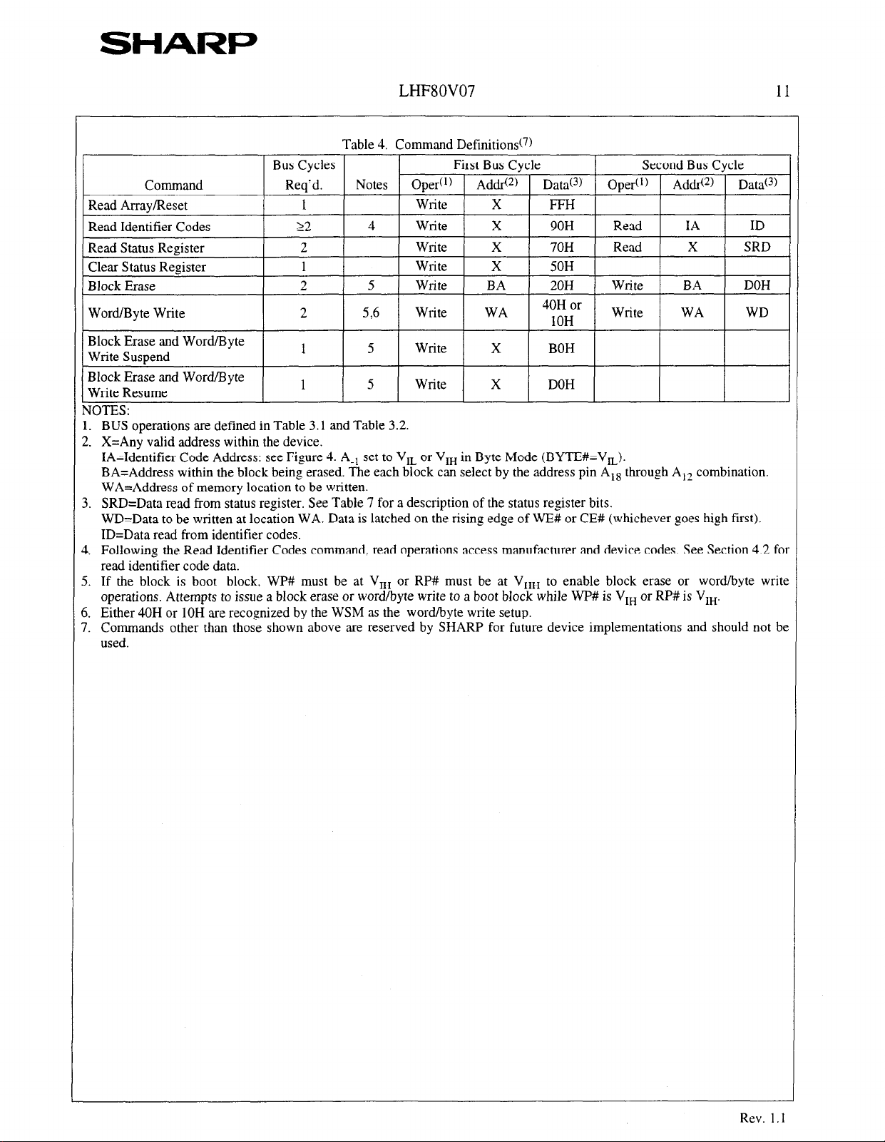
Table 4. Command Definitions(7)
NOTES:
1. BUS operations are defined in Table 3.1 and Table 3.2.
2. X=Any valid address within the device.
IA=Identifier Code Address: see Figure 4. A_, set to V,, or V,, in Byte Mode (BYTE#=V,,).
BA=Address within the block being erased. The each block can select by the address pin A,, through A,, combination.
WA=Address of memory location to be written.
3. SRD=Data read from status register. See Table 7 for a description of the status register bits.
WD=Data to be written at location WA. Data is latched on the rising edge of WE# or CE# (whichever goes high first).
ID=Data read from identifier codes.
4. Following the Read Identifier Codes command, read operations access manufacturer and device codes. See Section 4.2 foi
read identifier code data.
5. If the block is boot block, WP# must be at V, or RP# must be at V,, to enable block erase or word/byte write
operations. Attempts to issue a block erase or word/byte write to a boot block while WP# is V,, or RP# is V,,.
5. Either 40H or 1OH are recognized by the WSM as the word/byte write setup.
7. Commands other than those shown above are reserved by SHARP for future device implementations and should not be
used.
Page 14

SHARI=
LHF%OVO7
4.1 Read Array Command
Upon initial device power-up and after exit from deep
power-down mode, the device defaults to read array mode.
This operation is also initiated by writing the Read Array
command. The device remains enabled for reads until
another command is written. Once the internal WSM has
started a block erase or word/byte write. the device will
not recognize the Read Array command until the WSM
completes its operation unless the WSM is suspended via
an Erase Suspend or Word/Byte Write Suspend command.
The Read Array command functions independently of the
V,, voltage and RP# can be V,, or V,,.
4.2 Read Identifier Codes Command
The identifier code operation is initiated by writing the
Read Identifier Codes command. Following the command
write, read cycles from addresses shown in Figure 4
retrieve the manufacturer and device codes (see Table 5
for identifier code values). To terminate the operation,
write another valid command. Like the Read Array
command, the Read Identifier Codes command functions
independently of the V,, voltage and RP# can be V,, or
V,,. Following the Read Identifier Codes command, the
following information can be read:
Table 5. Identifier Codes
12
4.4 Clear Status Register Command
Status register bits SR.5, SR.4. SR.3 or SR.l are set tc
“1”s by the WSM and can only be reset by the Clear Statu:
Register command. These bits indicate various failure
conditions (see Table 7). By allowing system software tc
reset these bits, several operations (such as cumulatively
erasing multiple blocks or writing several words/bytes ir
sequence) may be performed. The status register may be
polled to determine if an error occurred during the
sequence.
To clear the status register, the Clear Status Register
command (50H) is written. It functions independently 01
the applied V,, Voltage. RP# can be V,, or V,,. This
command is not functional during block erase 01
word/byte write suspend modes.
4.5 Block Erase Command
Erase is executed one block at a time and initiated by a
two-cycle command. A block erase setup is first written.
followed by an block erase confirm. This command
sequence requires appropriate sequencing and an address
within the block to be erased (erase changes all block data
to FFFFH). Block preconditioning, erase? and verify are
handled internally by the WSM (invisible to the system).
After the two-cycle block erase sequence is written. the
device automatically outputs status register data when read
(see Figure 5). The CPU can detect block erase completion
by analyzing the output data of the RY/BY# pin or status
register bit SR.7.
4.3 Read Status Register Command
The status register may be read to determine when a block
:rase or word/byte write is complete and whether the
operation completed successfully. It may be read at any
ime by writing the Read Status Register command. After
writing this command, all subsequent read operations
output data from the status register until another valid
:ommand is written. The status register contents are
atched on the falling edge of OE# or CE#, whichever
occurs. OE# or CE# must toggle to V,, before further
.eads to update the status register latch. The Read Status
iegister command functions independently of the V,,
Joltage. RP# can be V,, or V,,.
When the block erase is complete, status register bit SR.5
should be checked. If a block erase error is detected. the
status register should be cleared before system software
attempts corrective actions. The CUI remains in read
status register mode until a new command is issued.
This two-step command sequence of set-up followed by
execution ensures that block contents are not accidentally
erased. An invalid Block Erase command sequence will
result in both status register bits SR.4 and SR.5 being set
to “1”. Also, reliable block erasure can only occur when
Vcc=2.7V-3.6V and VPP=VPPH1,2. In the absence of this
high voltage. block contents are protected against erasure.
If block erase is attempted while V,,IV,,,,, SR.3 and
SR.5 will be set to “1”. Successful block erase for boot
blocks requires that the corresponding if set, that
WP#=V,, or RP#=V,,. If block erase is attempted to
boot block when the corresponding WP#=V,, or
RP#=V,,, SR.l and SR.5 will be set to “1”. Block erase
operations with VIH<RP#<V,, produce spurious results
and should not be attempted.
Rev. 1.1
Page 15

SHARP
LHF8OVO7
4.6 Word/Byte Write Command
Word/byte write is executed by a two-cycle command
sequence.
alternate 10H) is written, followed by a second write that
specifies the address and data (latched on the rising edge
of WE#). The WSM then takes over, controlling the
word/byte write and write verify algorithms internally.
After the word/byte write sequence is written, the device
automatically outputs status register data when read (see
Figure 6). The CPU can detect the completion of the
word/byte write event by analyzing the RYlBY# pin or
status register bit SR.7.
When word/byte write is complete, status register bit SR.4
should be checked. If word/byte write error is detected, the
status register should be cleared. The internal WSM verify
only detects errors for “1”s that do not successfully write
to “0”s. The CUI remains in read status register mode until
it receives another command.
Reliable word/byte writes can only occur when
V,,=2.7V-3.6V and VPP=VPPHI,~. In the absence of this
high voltage, memory contents are protected against
word/byte writes. If word/byte write is attempted while
V,SV,,,, status register bits SR.3 and SR.4 will be set
to “1”. Successful word/byte write for boot blocks requires
that the corresponding if set, that WP#=V,, or RP#=V,,.
If word/byte write is attempted to boot block when the
corresponding WP#=V, or RP#=V,,, SR.1 and SR.4 will
be
V,<RP#<VN, p reduce spurious results and should not be
attempted.
Word/byte write setup (standard 40H or
set to ” 1”. Word/byte write operations with
13
4.7 Block Erase Suspend Command
The Block Erase Suspend command allows block-erase
interruption to read or word/byte write data in another
block of memory. Once the block-erase process starts,
writing the Block Erase Suspend command requests that
the WSM suspend the block erase sequence at a
predetermined point in the algorithm. The device outputs
status register data when read after the Block Erase
Suspend command is written. Polling status register bits
SR.7 and SR.6 can determine when the block erase
operation has been suspended (both will be set to “1”).
RY/BY# will also transition to High Z. Specification
twHRz2 defines the block erase suspend latency.
At this point, a Read Array command can be written to
read data from blocks other than that which is suspended.
A Word/Byte Write command sequence can also be issued
during erase suspend to program data in other blocks.
Using the Word/Byte Write Suspend command (see
Section 4.8), a word/byte write operation can also be
suspended. During a word/byte write operation with bIock
erase suspended, status register bit SR.7 will return to “0”
and the RY/BY# output will transition to VOL. However.
SR.6 will remain “1” to indicate block erase suspend
status.
The only other valid commands while block erase is
suspended are Read Status Register and Block Erase
Resume. After a Block Erase Resume command is written
to the flash memory, the WSM will continue the block
erase process. Status register bits SR.6 and SR.7 will
automatically clear and RY/BY# will return to VOL. After
the Erase Resume command is written, the device
automatically outputs status register data when read (see
Figure 7). V,, must remain at V,,,,,, (the same V,,
level used for block erase) while block erase is suspended.
RP# must also remain at Vr, or V,, (the same RP# level
used for block erase). WP# must also remain at V,, or V,,
(the same WP# level used for block erase). Block erase
cannot resume until wordlbyte write operations initiated
during block erase suspend have completed.
Rev. 1.1
Page 16

SHARI=
LHF8OV07 14
1
4.8 Word/Byte Write Suspend Command
The Word/Byte Write Suspend command allows
word/byte write interruption to read data in other flash
memory locations. Once the word/byte write process
starts, writing the Word/Byte Write Suspend command
requests that the WSM suspend the word/byte write
sequence at a predetermined point in the algorithm. The
device continues to
after the Word/Byte Write Suspend command is written.
Polling status register bits SR.7 and SR.2 can determine
when the word/byte write operation has been suspended
(both will be set to “1”). RY/BY# will also transition to
High Z. Specification twHRZl
suspend latency.
At this point, a Read Array command can be written to
read data from locations other than that which is
suspended. The only other valid commands while
word/byte write is suspended are Read Status Register and
Word/Byte Write Resume. After Word/Byte Write
Resume command is written to the flash memory. the
WSM will continue the word/byte write process. Status
register bits SR.2 and SR.7 will automatically clear and
RY/BY# will return to V,,. After the Word/Byte Write
Resume command is written, the device automatically
outputs
must remain at VPPH1,2 (the same V,, level used for
word/byte write) while in word/byte write suspend mode.
RP# must also remain at V,, or V,, (the same RP# level
used for word/byte write). WP# must also remain at VI, or
Vt, (the same WP# level used for word/byte write).
status
output
status register data when read
defines the word/byte write
register data when read (see Figure 8). V,,
4.10 Block Locking
This Boot Block Flash memory architecture features two
hardware-lockable boot blocks so that the kernel code for
the system can be kept secure while other blocks are
programmed or erased as necessary.
4.10.1
The V,, programming voltage can be held low for
complete write protection of all blocks in the flash device.
VPP=VIL for Complete Protection
4.102 WP#=V,, for Block Locking
The lockable blocks are locked when WP#=Vt,; any
program or erase operation to a locked block will result in
an error, which will be reflected in the status register. For
top configuration, the top two boot blocks are lockable.
For the bottom configuration. the bottom tow boot blocks
are lockable. Unlocked blocks can be programmed or
erased normally (Unless V,, is below VPPLK).
4.10.3 WP#=VIH for Block Unlocking
WP#=V,, unlocks all lockable blocks.
These blocks can now be programmed or erased.
WP# controls 2 boot blocks locking and V,, provides
protection against spurious writes. Table 6 defines the
write protection methods.
4.9 Considerations of Suspend
After the suspend command write to the CUI, read status
register command has to write to CUI, then status register
bit SR.6 or SR.2 should be checked for places the device
in suspend mode.
Table 6. Write Protection Alternatives
Operation
Block Erase
or
Word/Byte Write
VP,
VI,
‘vPPLK ‘HH
RP# WP#
x
VI,
‘1, , VI,
X All Blocks Locked.
X All Blocks Lock
X All Blocks Unlocked.
VI,
Effect
ted.
2 Boot Blocks Locked.
1 All Blocks Unlocked.
I
Rev. 1.1
Page 17

SHARI=
Table 7. Status Register Definition
WSMS 1 ESS
7 6
SR.7 = WRITE STATE MACHINE STATUS (WSMS)
1 = Ready
0 = Busy
SR.6 = ERASE SUSPEND STATUS (ESS)
1 = Block Erase Suspended
0 = Block Erase in Progress/Completed
SR.5 = ERASE STATUS (ES)
1 = Error in Block Erasure
0 = Successful Block Erase
SR.4 = WORD/BYTE WRITE STATUS (WBWS)
1 = Error in Word/Byte Write
0 = Successful Word/Byte Write
SR.3 = V, STATUS (VPPS)
1 = V,, Low Detect, Operation Abort
O=V,OK
SR.2 = WORD/BYTE WRITE SUSPEND STATUS
(WBWSS)
1 = Word/Byte Write Suspended
0 = Word/Byte Write in Progress/Completed
SR. 1 = DEVICE PROTECT STATUS (DPS)
1 = WP# or RP# Lock Detected, Operation Abort
0 = Unlock
ES 1 WBWS 1 VPPS 1 WBWSS
5 4
LIm3ovo7
Check RY/BY# or SR.7 to determine block erase or
word/byte write completion. SR.6-0 are invalid while
SR.7=“0”.
If both SR.5 and SR.4 are “1”s after a block erase attempt,
an improper command sequence was entered.
SR.3 does not provide a continuous indication of V,, level.
The WSM interrogates and indicates the V,, level only after
Block Erase or Word/Byte Write command sequences. SR.3
is not guaranteed to reports accurate feedback only when
vYY~vYY,ll2~
The WSM interrogates the WP# and RP# only after Block
Erase or Word/Byte Write command sequences. It informs
the system, depending on the attempted operation, if the
WP# is not V,,, RP# is not V,,.
3
1.5
( DPS R
2 1 0
NOTES:
SR.0 = RESERVED FOR FUTURE ENHANCEMENTS (R)
SR.0 is reserved for future use and should be masked out
when polling the status register.
Rev. 1.1
Page 18

SHARP
Block Address
Block Address
Check rf Desired
Erase Loop
LHF8OVO7
BUS
operatm
Read
Standby
Repeat for subsequent block ems”res.
Full status check can be done after each block uasc or after a sequrnce of
block crawrcs.
Command Commenls
Erase Setup
Daw=?OH
Addr=Wlthln Block to be Erased
Daa=DOH
Addr=Within Block Lo be Erased
Check SR.7
I=WSMReady
O=WSM Busy
16
R’LL STAR’S CHECK PROCEDLXE
Command
Standby
Standby
Standby
Standby
SR.5.SR.4.SR.3 and SR.1 us only cleared by tie clear Status
Register Command in cases where multiple blocks are erased
beforc full status is checked.
Check SR.3
l=Vpp Error Dctcct
Chzck SR.1
I=Devicz Protect Detect
Check SR.1.5
Both I=Command Ssquencc Error
Check SR.5
l=Block Erase Error
Commentr
Figure 5. Automated Block Erase Flowchart
Rev. 1.1
Page 19

SHARP
LHl-‘8UVU I I!
Start
Write IOH or 10H.
Address
wnrc WordAp
Data and Address
Full Status
Check If Deared
Word/Byte wms
Complete
FL-LL STATCS CHECK PROCEDL’RE
Read Status Reglstrr
Dala(See Above)
1
Suspnd Wwd/Byte
wrns Loop
BUS
Operation
Standby
Command
Setup Word/Byte Write
Word/Byte Wr,ts
Command
COlTl”X”lS
DnladOH cx 10H
Addr=Locat,on to Be Wrmen
Data=Data 10 Bc Wntwn
Addr=Loation to Be Wnttsn
Status Rep,ster Data
Check SR.7
I=WSM Ready
O=WSM Busy
.
CO”Ull?“lS
Check SR.?
,=VpP Error Dsr<cl
Standby
Sw,dby
SR.J.SR.3 and SR. I are only cleared by the Clear Status Rcg~stsr
command m cases where multiple locations are uwtten before
full S,P,U.X is checked.
Figure 6. Automated Word/Byte Write Flowchart
Check SR.1
I=Dcv,ce Praect Dstect
Check SR.?
I=Data Writs Error
Rev. 1.1
Page 20

SHARF’
LHF80V07
BUS
@erauon
Wrik
Read
Standby
Standby
Write
Command
Erase
Resume
18
Commcnls
Datn=BOH
Ad&=X
Star,,s Rzglstzr Data
Addr=X
Check SR.7
l=WSMReady
O=WSM Busy
Check SR.6
I=Block Erase Suspended
OeBlock Erase Completed
Data-WH
Addr-X
Figure 7. Block Erase Suspend/Resume Flowchart
Rev. 1.1
Page 21

SHARI=
LHF8OVO7
Writs BOW
Word/Byte write
Completed
BUS
operation
Read
Standby
Standby
Read
Command
Rad Array
Word/B)~c Write
Resume
Comments
Data=BOH
Ad&=X
Check SR.7
I=WSM Ready
C=WSM Busy
Check SR.?
I=Word/B~ze Wrltc Suspended
O=Word/B>zc Writs Completed
Data=FFH
Ad&=X
Daa=DOH
Addr=X
Word/Byte Writs
Resumed
Figure 8. Word/Byte Write Suspend/Resume Flowchart
Rev. 1.1
Page 22

SIiARl=
LHF80V07
5 DESIGN CONSIDERATIONS
5.1 Three-Line Output Control
The device will often be used in large memory arrays.
SHARP provides three control inputs to accommodate
multiple memory connections. Three-line control provides
for:
a. Lowest possible memory power dissipation.
b. Complete assurance that data bus contention will not
occur.
To use these control inputs efficiently, an address decoder
should enable CE# while OE# should be connected to all
memory devices and the system’s READ# control line.
This assures that only selected memory devices have
active outputs while deselected memory devices are in
standby mode. RP# should be connected to the system
POWERGOOD signal to prevent unintended writes during
system power transitions. POWERGOOD should aiso
toggle during system reset.
5.2 RY/BY#, Block Erase and Word/Byte
Write Polling
RYlBY# is an open drain output that should be connected
to V,, by a pull up resistor to provide a hardware method
of detecting block erase and word/byte write completion.
It transitions low after block erase or word/byte write
commands and returns to High Z when the WSM has
finished executing the internal algorithm.
5.3 Power Supply Decoupling
Flash memory power switching characteristics require
careful device decoupling. System designers are interested
in three supply current issues; standby current levels.
active current levels and transient peaks produced by
falling and rising edges of CE# and OE#. Transient currenl
magnitudes depend on the device outputs’ capacitive and
inductive loading. Two-line control and proper decoupling
capacitor selection will suppress transient voltage peaks.
Each device should have a O.lpF ceramic capacitor
connected between its V,, and GND and between its V,,
and GND. These high-frequency. low inductance
capacitors should be placed as close as possible to package
leads. Additionally, for every eight devices, a 4.7pF
electrolytic capacitor should be placed at the array’s power
supply connection between V,, and GND. The bulk
capacitor will overcome voltage slumps caused by PC
board trace inductance.
5.4 Vpp Trace on Printed Circuit Boards
Updating flash memories that reside in the target system
requires that the printed circuit board designer pay
attention to the V,,
supplies the memory cell current for word/byte writing
and block erasing. Use similar trace widths and layout
considerations given to the V,, power bus. Adequate V,,
supply traces and decoupling will decrease V,, voltage
spikes and overshoots.
Power supply trace. The V,, pin
RY/BY# can be connected to an interrupt input of the
system CPU or controller. It is active at all times. RY/BY#
IS also High Z when the device is in block erase suspend
(with word/byte write inactive), word/byte write suspend
Jr deep power-down modes.
Rev. 1.1
Page 23

SHARP
LHF8OVO7
5.5 VCC, Vpp, RP#
Block erase and word/byte write are not guaranteed if V,,
falls outside of a valid VPPHIR range, V,, falls outside of
a valid 2.7V-3.6V range. or RP##V,, or V,,. If V,, error
is detected, status register bit SR.3 is set to “1” along with
SR.4 or SR.5, depending on the attempted operation. If
RP# transitions to V,, during block erase or word/byte
write, RY/BY# will remain low until the reset operation is
complete. Then, the operation will abort and the device
will enter deep power-down. The aborted operation may
leave data partially altered. Therefore, the command
sequence must be repeated after normal operation is
restored. Device power-off or RP# transitions to V, clear
the status register.
The CUI latches commands issued by system software and
is not altered by V,, or CE# transitions or WSM actions.
Its state is read array mode upon power-up, after exit from
deep power-down or after V,, transitions below VLKO.
After block erase or word/byte write, even after V,,
transitions down to V,,,, the CUI must be placed in read
array mode via the Read Array command if subsequent
access to the memory array is desired.
Transitions
5.6 Power-Up/Down Protection
The device is designed to offer protection against
lccidental block erasure or word/byte writing during
power transitions. Upon power-up, the device is
indifferent as to which power supply (V,, or V,,)
?owers-up first. Internal circuitry resets the CUI to read
u-ray mode at power-up.
21
A system designer must guard against spurious writes for
V,, voltages above V,,, when V,, is active. Since botlWE# and CE# must be low for a command write, driving
either to V,, will inhibit writes. The GUI’s two-stey
command sequence architecture provides added level o
protection against data alteration.
WP# provide additional protection from inadvertent cod<
or data alteration. The device is disabled while RP#=V,,
regardless of its control inputs state.
5.7 Power Dissipation
When designing portable systems. designers must considel
battery power consumption not only during device
operation, but also for data retention during system idle
time. Flash memory’s nonvolatility increases usable
battery life because data is retained when system power is
removed.
In addition, deep power-down mode ensures extremely
low power consumption even when system power is
applied. For example, portable computing products and
other power sensitive applications that use an array of
devices for solid-state storage can consume negligible
power by lowering RP# to V, standby or sleep modes. If
access is again needed, the devices can be read following
the fPHQV and tPHWL
first raised to VIH. See AC Characteristics- Read Only
and Write Operations and Figures 11, 12> 13 and 14 for
more information.
wake-up cycles required after RP# is
Rev. 1.1
Page 24

SHARP
LHF8OVO7 22
6 ELECTRICAL SPECIFICATIONS
6.1 Absolute Maximum Ratings*
Operating Temperature
During Read, Block Erase and
Word/Byte Write . . . . . . . . . . . . . . . . . . . . . . . . . . . . . . . . . 0°C to +7O”C(r)
Temperature under Bias . . . . . . . . . . . . . . . . . . . . . . - 10°C to +SO”C
Storage Temperature . . . . . . . . . . . . . . . . . . . . . . . . . . . . . . . . -65°C to +125”C
Voltage On Any Pin
(except V,,, V,,, and RP#) . . . . . . . . . . . . -0.5V to +7.OV(*)
V,, Supply Voltage . . . . . . . . . . . . . . . . . . . . . . . . . . . . . . . . -0.2V to +7.OV(*)
V,, Update Voltage during Block
Erase and Word/Byte Write . . . . . . . . . -0.2V to +l 4.0V(2,3)
RP# Voltage _....................................... -0.5V to +14.0V(*y3)
Output Short Circuit Current . . . . . . . . . . . . . . . . . . . . . . . . . . . . . . . . 100mA(4)
6.2 Operating Conditions
*WARNING: Stressing the device beyond the “Absolute
Maximan Ratings” may cause permanent damage. These
are stress ratings only. Operation beyond the “Operating
Conditions” is not recommended and extended exposure
beyond the “Operating Conditions” may affect device
reliability.
NOTES:
1. Operating temperature is for commercial temperature
product defined by this specification.
2. All specified voltages are with respect to GND.
Minimum DC voltage is -0SV on input/output pins
and -0.2V on V,,
this level may undershoot to -2.OV for periods <20ns.
Maximum DC voltage on input/output pins and V,, is
V,,+OSV which, during transitions, may overshoot to
Vcc+2.0V for periods <20ns.
3. Maximum DC voltage on V,, and RP# may overshoot
to +14.OV for periods <20ns.
4. Output shorted for no more than one second. No more
than one output shorted at a time.
and V,, pins. During transitions,
Temperature
Symbol Parameter Min. Max.
TA
vcc
Operating Temperature 0 +70 “C
Vcc Supply Voltage (2.7V-3.6V)
2.7 3.6 V
5.2.1 CAPACITANCE( *)
T,=+25”C, f=lMHz
Symbol Parameter
cIN
‘OUT
VOTE:
I. Sampled, not 100% tested.
Input Capacitance 7 10
Output Capacitance
TYP.
9 12
Max. Unit Condition
Unit Test Condition
Ambient Temperature
PP
PP
v,,=o.ov
v,U,=o.ov
Rev. 1.1
Page 25

SHARP
LHF8OVO7
6.2.2 AC INPUT/OUTPUT TEST CONDITIONS
AC test inputs are driven at 2.7V for a Logic “1” and O.OV for a Logic “0.” Input timing begins, and output timing ends, at 1.35V.
Input rise and fall times (107~ to 90%) ~10 ns.
Figure 9. Transient Input/Output Reference Waveform for V,,=2.7V-3.6V
lN914
Test Confieuration Caoacitance Loading Value
Test Configuration
Vcc=2.7V-3.6V 30
C,(pF)
23
CL Includes Jig
Capacitance
Figure 10. Transient Equivalent Testing Load
Circuit
Rev. 1.1
Page 26

SHARI=
6.2.3 DC CHARACTERISTICS
Sym. Parameter Notes
IL1
IL0
kcs
‘CCD
‘CCR
ICC,
‘CC,
kcws
‘CCES
IPPS
‘PPR
‘PPD
IPPW
‘PPE
IPPWS
‘PPES
Input Load Current 1
Output Leakage Current 1
V,, Standby Current
V,, Deep Power-Down Current 1,lO
V,, Read Current
V,, Word/Byte Write Current
V,, Block Erase Current
V,, Word/Byte Write or
Block Erase Suspend Current
V, Standby or Read Current
VP, Deep Power-Down Current
VP, Word/Byte Write Current
V, Block Erase Current
VP, Word/Byte Write or 1
Block Erase Suspend Current
LHF80V07 24
DC Characteristics
V,,=27V-3.6V Test
TYP.
1,336,
10 25 50
1,3,6
0.2
5 10
1,596
15
137
5 17 mA
5 12
1,7
4
4 12 nL4
12
1
1 6 mA CE#=V,
+2 &15
10 200
1 0.1 5
1,7
177
12 40
8 25
10 200
Max.
*OS
*OS
2 mA VCC=VCCMax.
25
30 mA
17
30
20
Unit Conditions
11A
VCC=VCCMax.
V,,=V,, or GND
cul\ p=w-
OUT=VCC or GND
CMOS Inputs
ClA
Vcc=VccMax.
CE#=RP#=V,,&2V
TTL Inputs
CE#=RP#=V,,
RP#=GND*0.2V
llA
IoUT(RY/13Y#)=OmA
CMOS Inputs
mA V,,=V,,Max., CE#=GND
f=SMHz, I,,,=OmA
TlL Inputs
VCC=VCCMax., CE#=GND
f=SMHz. IoUT=OmA
V,,=2.7V-3.6V
mA V,,=11,4V-12.6V
mA V,,=2.7V-3.6V
V,,=11.4V-12.6V
PA
PA
I.rA
VPP~VCC
vPP’vcc
RP#=GND+0.2V
mA Vpp=2.7V-3.6V
mA VP,=1 1.4V- 12.6V
mA Vpp=2.7V-3.6V
mA Vpp=11.4V-12.6V
ClA
VPP=VPPHI I2
Rev. 1.1
Page 27

SHARI=
LHF8OVO7
25
DC Characteristics (Continued)
Vo=2.7V-3.6V
Sym.
V,, Low Voltage Input
VIH
VOL
‘OHI
Input High Voltage
Output Low Voltage
Output High Voltage
Cl-rL)
‘OH2
VPPLK
‘PPHl
‘PPH2
VHH
Output
(CMOS)
V, Lockout Voltage during Normal 4,7
Operations
V, Voltage during Word/Byte Write
or Block Erase Operations
VP, Voltage during Word/Byte Write
or Block Erase Operations
RP# Unlock Voltage 83
Parameter Notes Min.
7 -0.5 0.8
7
337
3.7
High Voltage
3,7
Max.
2.0
+“,c?
0.4
2.4
0.85
Vcc
2%
1.5
2.7 3.6
11.4 12.6
2.0
11.4
12.6
Unit Test Conditions
V
V
yccz;=~in.
V
V
V
V
OL
ycc~pccin~
OH- .
;CflCdMin.
OH .
Vcc=Vcc Min.
IoH’- lOOpA
V
V
V
V
V Unavailable WP#
NOTES:
1. All currents are in RMS unless otherwise noted. Typical values at nominal V,, voltage and T,=+25”C.
2. ICC,, md ‘CCES
are specified with the device de-selected. If read or wordlbyte written while in erase suspend mode, the
device’s current draw is the sum of Iccws or ICCES and ICCR or ICC,, respectively.
3. Includes RY/BY#.
4. Block erases and word/byte writes are inhibited when VppIVppLK,
and not guaranteed in the range between VppLK(max.)
and VppHl(min.), between VppHl(max.) and VppH2(min.) and above VppH2(max.).
5. Automatic Power Savings (APS) reduces typical ICC,
to 3mA at 2.7V V,, in static operation.
6. CMOS inputs are either Vcc&0.2V or GNDk0.2V. TTL inputs are either V,, or V,,.
7. Sampled, not 100% tested.
8. Boot block erases and word/byte writes are inhibited when the corresponding RP#=V,, and WP#=Vl,. Block erase and
word/byte write operations are not guaranteed with VrH<RP#<VH, and should not be attempted.
9. RP# connection to a V,,
supply is allowed for a maximum cumulative period of 80 hours.
10. BYTE# input level is Vcc&.2V in word mode or GND+-0.2V in byte mode. WP# input level is Vcck0.2V or GNDti.2V.
Rev. 1.1
Page 28

SHARP
LHF8OVO7 26
6.2.4 AC CHARACTERISTICS - READ-ONLY OPERATIONS(l)
NOTES:
1.
See AC Input/Output Reference Waveform for maximum allowable input slew rate.
2.
OE# may be delayed up to tELQV-bLQV
3. Sampled, not 100% tested.
4. If BYTE# transfer during reading cycle, exist the regulations separately.
after the falling edge of CE# without impact on tELQv.
Rev. 1.1
Page 29

SHARI=
VIH
iDDRESSES
OE#(G)
:“I--
WE#(W)
hi f-----
VOH
DATA(D/Q)
(DQo-DQd
VOL
VIL
Standby
HIGH Z
Device
Address Selection
Address Stable
4
I
tAVQV
Llw8OVO7
b
27
Data Valid
--;~j HIGH Z
“cc
VIH I
~#(P)
VIL
tPHQV
-----------7
Figure 11. AC Waveform for Read Operations
Rev. 1.1
Page 30

SHARP
II
.DDRESSES(A)
OE#(G)
BYTE#(Fj
DATA(D/Q)
(DQo-DQ7)
VIH
VIL
y---
VIH
VtL
VOH
VOL
Standby
HIGH Z
Device
Address Selection
4
Address Stable
LHF8OVO7
Data Valid
28
____-______
_______----
___________
___-_-_----
VOH
DATA(D/Q)
(DQs-DQls)
VOL
HIGH Z
Data
output
Figure
12. BYTE# timing Waveform
HIGH Z
Rev. I.1
Page 31

SHARP
LHFSOV07
6.2.5 AC CHARACTERISTICS - WRITE OPERATIONS(l)
29
NOTES:
1.
Read timing characteristics during block erase and word/byte write operations are the same as during read-only operations.
Refer to AC Characteristics for read-only operations.
2. Sampled, not 100% tested.
3. Refer to Table 4 for valid A,, and D,, for block erase or word/byte write.
4. V,, should be held at V,,,t,z (and if necessary RP# should be held at V,,) until determination of block erase or
word/byte write success (SR.1/3/4/5=0).
5. If BYTE# switch during reading cycle, exist the regulations separately.
Rev. 1.1
Page 32

SHARP
ADDRESSES(A)
CE#(E)
OE#(Gl
WE#(W)
DATA(D/Ql
BYTE#(F)
RY/BY#(R)
LHF80V07
30
WPW)
VHH
RPNP)
VIH .-
vppw
NOTES:
1. V,-c power-up and standby.
2. Write block erase or word/byte write setup.
3. Write block erase confirm or valid address and data
4. Automated erase or program delay.
5. Read status register data.
6. Write Read Array command.
Figure 13. AC Waveform for WE#-Controlled Write Operations
bHHWH ,
Rev. 1.1
Page 33

SHARP
LHF8OVO7
6.2.6 ALTERNATIVE CE#-CONTROLLED WRITES(l)
NOTES:
1.
In systems where CE# defines the write pulse width (within a longer WE# timing waveform), all setup. hold, and inactive
WE# times should be measured relative to the CE# waveform.
2. Sampled, not 100% tested.
3.
Refer to Table 4 for valid A,, and D,, for block erase or word/byte write.
4. V,, should be held at V,,,,,, (
word/byte write success (SR.1/3/4/5=0).
5. If BYTB# switch during reading cycle, exist the regulations separately.
and if necessary RP# should be held at V,,) until determination of block erase or
Rev. 1.1
Page 34

SHARI=
ADDRESSES(A)
CE#(E)
OE#(G)
WEKW)
DATA(D/Q)
BYTE#(F)
RY/BY#(R)
VIH
VIL
VIH
VIL
VIH
VIH
LHFSOV07
32
WP#(S)
RPMP)
NO-l-ES:
1. VCC power-up and standby.
2. Write block erase or word/byte write setup.
3. Write block erase confirm or valid address and data.
4. Automated erase or program delay
5. Read status register data.
6. Write Read Array command
VIH ,‘
Figure 14. AC Waveform for CE#-Controlled Write Operations
Rev. 1.1
Page 35

SHARP
RESET OPERATIONS
LHF8OVO7
RY/BY#(R)
RP#(P)
RY/BY#(R)
RP#(P)
vcc
RP#(P)
VOL
VIH
VU
High Z
VOL
VIH
VIL
2.w
VU
VIH
VIL
(A)Reset During Read Array Mode
(B)Reset During Block Erase or Word/Byte Write
L
I
- hVPH -
i
(C)RP# rising Timing
Figure 15. AC Waveform for Reset Operation
Reset AC Specifications
V,,=2.7V-3.6V
Sym. Parameter Notes Min.
RP# Pulse Low Time
‘PLPH
tPLRZ
t2VPH
(If RP# is tied to V,,. this specification is not applicable)
RP# Low to Reset during Block Erase or Word/Byte Write
12
Vcc 2.7V to RP# High 3 100
100
Max. Unit
ns
22
P
ns
VOTES:
1. If RP# is asserted while a block erase or word/byte write operation is not executing, the reset will complete within loons.
!. A reset time, tpHQVz is required from the later of RY/BY# going High Z or RP# going high until outputs are valid.
3. When the device power-up, holding RP# low minimum IOOns is required after V,,
has been in predefined range and also
has been in stable there.
Rev. 1.1
Page 36

SHARP
LHF8OVO7 34
6.2.8 BLOCK ERASE AND WORD/BYTE WRITE PERFORMANCE(3)
NOTES:
1. Typical values measured at T,=+25”C and nominal voltages. Subject to change based on device characterization.
2. Excludes system-level overhead.
3. Sampled but not 100% tested.
4. All values are in word mode (BYTE#=V,,). At byte mode (BYTE#=V,,), those values are double.
Rev. 1.1
Page 37

SHARP
__.__.______...__.__~~..~~~~~---~~~~-~~~~..-~~~.-.--~--~~~~~~..~~~~~~~~...~~~~~~~~..---~~~~~~~~--~~~~~~~-~~~~~--~~~~~~~-~~~~~.~~~....----~.--------.---------
_.__________.___________________________~~~~~~~~~~..~~~~~~~~~~~~~~~~~~~~~~~~~~~~~~~~~~~~~~~~~~~~~~~~~~~~~~.~.~~~~~~~~~~~~~~~~~~~~~~~~~~.~~~~~~...~~~~~...~~~~
_.__________________-~.~~~~~-~~~~~--~~~...-~~...----.-~-~~~~...~~~~~~~~.--~~~~~~~~..-~~~~~~~~~~--~~~~~~~-~~~~~-~~~~~~--~~~~..-~~~~.------...-------..--------
_.._______._.__._....~~~....~~~-.~~~~~~~~~~-~~~~...-~~~~--~-~~~~-~~-~~~~~~~~~-~--~~~~~~~-~-~.~~~~~---~~~~..~~~~~~~.~~~~~~--~~~~~-~~~~..-~~~~..-----...-------
7 Package and packing specification
1. Package Outline Specification
Refer to drawing No.AA2 0 3 4
2. Markings
2 - 1. Marking contents
( 1) Product name : F800BVB-
(2) Company name : SHARP
( 3 ) Date code
(Example) Y Y Indicates the product was manufactured
(4) The marking of “JAPAN” indicates the count
2-2. Marking layout
Refer to drawing No.AA2 0 3 4
(This layout does not define the dimensions of marki
TTLSO
LHF80V07
- Denotes the production ref.code (l-3)
in the WWth week of 19YY.
Denotes the production week.
(01,02,03, . . . * . 52,53)
Denotes the production year.
(Lower
two digits of the year.)
ry of origin.
ng character and marking position.)
35
3. Packing Specification (Dry packing for surface mount packages)
Dry packing is used for the purpose of maintaining IC quality after mounting
packages on the PCB (Printed Circuit Board).
If the surface mount type package absorbs a large amount of moisture,
this moisture may suddenly vaporize into steam when the entire package is heated
during the reflow soldering process. This causes expansion and results
in separation between the resin and insert material, and sometimes cracking
of the package. This dry packing is designed to prevent the above problem
from occurring in surface mount packages.
3 - 1 . Packing Materials
Mater ial Name Material Specificaiton
Tray Conductive plastic(lOOdevices/tray) Fixing of device
___..________._.____.~~~~~~.~~~~..~~~~~-~~~~~-~~~~...-~~~~..---~~~~..-----~~~.~-.---~~~~~~~..-~~~~~~.~~~~~.~~~~~~.-~~~~~.------------------------ --------
Upper cover tray
Laminated aluminum bag Aluminum polyethylene (lbag/case)
Des iccant Silica gel Drying of device
P P band
__________-_.____.---~.~~~-~~~~~~-~~~~~..--~~..-----.---~~~....~-~~~~~~~..---~~~~~~~~~----~~~~~~~-~~-~~
Inner case Card board (lOOOdevices/case) Packaging of device
_________._______----~~~~~--~~~.--~~~~..---...-------~~~....---~~.....----~~~~....---~~~~~~..~~-~~~~~..-- ___----____----____.-~~~...----...-------.---------
Label
Outer case Card board Outer packing of tray
(Devices shall be placed into a tray in the same direction.)
Conductive plast ic (It ray/case)
Polypropylene
Paper
(5pcs/case) Fixing of tray
Purpose
Fixing of device
Drying of device
__.._____________---____________________---~~~..------
Indicates part number,quantity
and date of manufacture
Page 38

SHARP
3-2. Outline dimension of tray
Refer to attached drawing
Storage and Opening of Dry Packing
4.
LHF80V07
36
4-l. Store under conditions shown below befo
(1) Temperature range
(2) Humidity
4-2. Notes on opening the dry packing
(1) Before opening the dry packing, prepare a working table which is
grounded against ESD and use a grounding strap.
(2) The tray has been treated to be conductive or anti-static. If the
device is transferred to another tray, use a equivalent tray.
4-3. Storage after opening the dry packing
Perform the following to prevent absorption of moisture after opening.
(1) After opening the dry packing, store the ICs in an environment with
a temperature of 5--25°C and a relative humidity of 60% or less.
If doing reflow soldering once, mount ICs within 4 days after the opening.
If doing reflow soldering twice, do the first mounting within
4 days after the opening and do the second mounting within
4 days after the first mounting.
(2) To re-store the ICs for an extended period of time within 4 days after
opening the dry packing,
packing with desiccant (whoes indicater is blue), and store in an
environment with a temperature of 5-40°C and a relative humidity of
80% or less, and mount ICs within 2 weeks.
(3) Total period of storage after first opening and re-opening is within
4 days, and store the ICs in the same environment as sect ion 4-3. (I).
: 5-40°C
: 80% RH or less
use a dry box or re-seal the ICs in the dry
re opening the dry pack i
ng
First opening+ XI +re-sealing+ Y -‘re-opening- Xz
V
ICs in dry
packing
4 - 4. Baking (drying) before mounting
(1) Baking is necessary
(A) If the humidity indicator in the desiccant becomes pink
(B) If the procedure in section 4-3 could not be performed
(2) Recommended baking conditions
If the above conditions (A) and (B) are applicable, bake it before
mounting, The recommended conditions are 1-3 hours at 120 ~~““C.
Heat resistance tray is used for shipping tray.
(3) Storage after baking
After baking ICs, store the ICs in the same environment as sect ion
4-3. (1).
5-25°C 5-40°C
60%RH or less SO%RH or less 60%RH or less
5-25°C
-mount
ing
Page 39

SHARP
5. Surface Mount Conditions
Please perform the following conditions when mounting ICs not to deteriorate IC
quality.
LHF80V07
37
5-l.
,Soldering conditions
Mounting Method
Reflow soldering
5- 2. Conditions for removal of residual flux
(1) Ultrasonic washing power : 25 Watts/liter or less
(2) Washing time
( 3 > Solvent temperature
Temperature and Duration Measurement Point
Peak temperature of 240°C or less, IC package surface
duration of less than 15 seconds above
230°C. 200°C or over ,durat ion of
30-50 seconds. Preheat temperature
of 125~150°C duration of less than
180 seconds. Temperature increase
rate of l--4”C/second.
: Total 1 minute maximum
: 15-40°C
,
J
Page 40

SHARF’
LHF80V07
TOP VIEW------
I
,I NDEX
v
F8OOBVB-
TTLSO JAPAN
---_
-:’
I
I
I
0
\
\
\
\
\
\
‘.
--___-y .
1
.’
/
’ 0
A-l
\
I I\
/
\
\
J(
I
I
I
0. 4
T’TF.
a
p_
-- BOTTOM VIEW
I
I
t
I
,z- @@0.15@
%lq tB%
NAME ;
DRAWING NO. i AA2034
FBGA048-P-0808 NOTE
%iM I
UNIT ! mm
- $ 60. 30
1. 2
TYP.
cbo.45 20.03
01
@ S AB
SCD
Page 41

SHARP
-r
-
h
:
C
f
A
1
LHF80V07
a
p.3
5.8 r
!7.9
25.0~0.3*4=100.0~0.3
%vF~ fiiwi
JAME 1 LCSP80-0808TCT-RH NOTE
i+.&{Z ;
DRAWING NO. / CV812 UNIT 1 mm
I
35.8
17.4
2::
w
Page 42

SHARf=
LHE3OVO7
Flash memory LHFsOV(B)XX family Data Protection (TSOP
Noises having a level exceeding the limit specified in the specification may be
generated under specific operating conditions on some systems.
Such noises, when induced onto WE# signal or power supply, may be interpreted as false
commands, causing undesired memory updating.
To protect the data stored in the flash memory against unwanted overwriting, systems
operating with the flash memory should have the following write protect designs, as
appropriate:
1) Protecting data in specific block
By setting a WP# to low, only the boot block can be protected against overwriting.
Parameter and main blocks cannot be locked.
System program, etc.,
When a high voltage is applied to RP#, overwrite operation is enabled for all blocks.
can be locked by storing them in the boot block.
package, CSP package)
40
For further information on controlling of WP# and RP#, refer to the specification.
(See chapter 4.10)
2) Data protection through Vpp
When the level of Vpp is lower than VPPLK (lockout voltage), write operation on the
flashmemory is disabled. All blocks are lockedandthedata intheblocksarecompletely
write protected.
For the lockout voltage, refer to the specification. (See chapter 4.10 and 6.2.3. >
3) Data protection through RP#
When the RP# is kept low during power up and power down sequence such as voltage
transition, write operation on the flash memory is disabled, write protecting all
blocks.
For the detai 1s of RP# control, refer to the specification. (See chapter 5.6 and 6.2.7. >
4) Noise rejection of WE#
Consider noise rejection of WE# in order to prevent false write command input.
Rev 1.1
 Loading...