

Datasheet LH28F800BGR-TL85, LH28F800BGR-TL12, LH28F800BGR-BL85, LH28F800BGR-BL12, LH28F800BGHR-TL85 Datasheet (Sharp)
...Page 1
LH28F800BG-L/BGH-L (FOR TSOP, CSP)
8 M-bit (512 kB x 16) SmartVoltage
LH28F800BG-L/BGH-L
(FOR TSOP, CSP)
DESCRIPTION
The LH28F800BG-L/BGH-L flash memories with
SmartVoltage technology are high-density, low-cost,
nonvolatile, read/write storage solution for a wide
range of applications. The LH28F800BG-L/BGH-L
can operate at V
low voltage operation capability realizes longer
battery life and suits for cellular phone application.
Their boot, parameter and main-blocked
architecture, flexible voltage and enhanced cycling
capability provide for highly flexible component
suitable for portable terminals and personal
computers. Their enhanced suspend capabilities
provide for an ideal solution for code + data storage
applications. For secure code storage applications,
such as networking, where code is either directly
executed out of flash or downloaded to DRAM, the
LH28F800BG-L/BGH-L offer two levels of protection
: absolute protection with V
hardware boot block locking. These alternatives
give designers ultimate control of their code security
needs.
CC = 2.7 V and VPP = 2.7 V. Their
PP at GND, selective
FEATURES
• SmartVoltage technology
– 2.7 V, 3.3 V or 5 V V
– 2.7 V, 3.3 V, 5 V or 12 V VPP
• High performance read access time
LH28F800BG-L85/BGH-L85
– 85 ns (5.0±0.25 V)/90 ns (5.0±0.5 V)/
100 ns (3.3±0.3 V)/120 ns (2.7 to 3.6 V)
LH28F800BG-L12/BGH-L12
– 120 ns (5.0±0.5 V)/130 ns (3.3±0.3 V)/
150 ns (2.7 to 3.6 V)
• Enhanced automated suspend options
– Word write suspend to read
– Block erase suspend to word write
– Block erase suspend to read
CC
• Enhanced data protection features
– Absolute protection with V
– Block erase/word write lockout during power
transitions
– Boot blocks protection with WP# = V
• SRAM-compatible write interface
• Optimized array blocking architecture
– Two 4 k-word boot blocks
– Six 4 k-word parameter blocks
– Fifteen 32 k-word main blocks
– Top or bottom boot location
• Enhanced cycling capability
– 100 000 block erase cycles
• Low power management
– Deep power-down mode
– Automatic power saving mode decreases I
in static mode
• Automated word write and block erase
– Command user interface
– Status register
TM
∗
• ETOX
• Packages
– 48-pin TSOP Type I (TSOP048-P-1220)
– 48-ball CSP (FBGA048-P-0808)
∗ ETOX is a trademark of Intel Corporation.
V nonvolatile flash technology
Normal bend/Reverse bend
Flash Memories
PP = GND
IL
CC
In the absence of confirmation by device specification sheets, SHARP takes no responsibility for any defects that may occur in equipment using any SHARP devices shown in catalogs, data books,
etc. Contact SHARP in order to obtain the latest device specification sheets before using any SHARP device.
- 1 -
Page 2
A2
1
A
A
3B
A
1C
A
0D
GND
E
CE#
A5
2
A
6
A4
OE#
DQ8
DQ0
A17
WP# WE#
3
A
7
DQ1
DQ2
DQ9
4
VPP
DQ10
DQ11
DQ3
5
RP#
NC
DQ12
VCC
DQ4
A8
6
NC
A9
DQ6
DQ5
DQ13
A11
7
A10
A12
DQ15
DQ14
DQ7
A14
8
A13
A15
A16
GND
NC
F
RY/BY#
A18
(FBGA048-P-0808)
48-BALL CSP48-PIN TSOP (Type I)
(TSOP048-P-1220)
A15
A14
A13
A12
A11
A10
A9
A8
NC
NC
WE#
RP#
V
PP
WP#
RY/BY#
A
18
A17
A7
A6
A5
A4
A3
A2
A1
1
2
3
4
5
6
7
8
9
10
11
12
13
14
15
16
17
18
19
20
21
22
23
24
48
47
46
45
44
43
42
41
40
39
38
37
36
35
34
33
32
31
30
29
28
27
26
25
A16
NC
GND
DQ
15
DQ7
DQ14
DQ6
DQ13
DQ5
DQ12
DQ4
VCC
DQ11
DQ3
DQ10
DQ2
DQ9
DQ1
DQ8
DQ0
OE#
GND
CE#
A
0
COMPARISON TABLE
VERSIONS
LH28F800BG-L
(FOR TSOP, CSP)
LH28F800BGH-L
(FOR TSOP, CSP)
LH28F800BG-L
(FOR SOP)
∗1 Refer to the datasheet of LH28F800BG-L (FOR SOP).
OPERATING
TEMPERATURE
0 to +70°C
– 40 to +85°C
1
∗
PACKAGE
48-pin TSOP (I)
48-ball CSP WP# and
48-pin TSOP (I)
48-ball CSP WP# and
0 to +70°C 44-pin SOP 10 µA Controlled by RP# pin
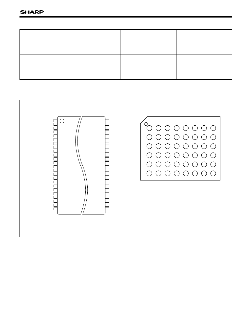
PIN CONNECTIONS
LH28F800BG-L/BGH-L (FOR TSOP, CSP)
DC CHARACTERISTICS
VCCdeep power-down current (MAX.)
10 µA
20 µA
WRITE PROTECT FUNCTION
FOR BOOT BLOCKS
Controlled by
Controlled by
RP# pins
RP# pins
TOP VIEW
NOTE :
Reverse bend available on request.
- 2 -
Page 3
BLOCK ORGANIZATION
INPUT
BUFFERBUFFER
OUTPUT
MULTIPLEXER
VCC
CE#
RP#
OE#
IDENTIFIER
REGISTER
COMMAND
USER
INTERFACE
WRITE
STATE
MACHINE
PROGRAM/ERASE
VOLTAGE SWITCH
I/O
LOGIC
STATUS
REGISTER
DATA
REGISTER
DATA
COMPARATOR
15
32 k-WORD
MAIN BLOCKS
X
DECODER
Y
DECODER
Y GATING
RY/BY#
V
PP
V
CC
GND
A0-A18
INPUT
BUFFER
ADDRESS
LATCH
ADDRESS
COUNTER
BOOT BLOCK 0
BOOT BLOCK 1
PARAMETER BLOCK 0
PARAMETER BLOCK 1
PARAMETER BLOCK 2
PARAMETER BLOCK 3
PARAMETER BLOCK 4
PARAMETER BLOCK 5
MAIN BLOCK 0
MAIN BLOCK 1
MAIN BLOCK 13
MAIN BLOCK 14
WP#
WE#
OUTPUT
DQ0-DQ15
This product features an asymmetrically-blocked
architecture providing system memory integration.
Each erase block can be erased independently of
the others up to 100 000 times. For the address
locations of the blocks, see the memory map in
Fig. 1.
Boot Blocks : The two boot blocks are intended to
replace a dedicated boot PROM in a microprocessor or microcontroller-based system. The
boot blocks of 4 k words (4 096 words) feature
hardware controllable write-protection to protect the
crucial microprocessor boot code from accidental
modification. The protection of the boot blocks is
controlled using a combination of the V
PP, RP# and
WP# pins.
BLOCK DIAGRAM
LH28F800BG-L/BGH-L (FOR TSOP, CSP)
Parameter Blocks : The boot block architecture
includes parameter blocks to facilitate storage of
frequently update small parameters that would
normally require an EEPROM. By using software
techniques, the byte-rewrite functionality of
EEPROMs can be emulated. Each boot block
component contains six parameter blocks of 4 k
words (4 096 words) each. The parameter blocks
are not write-protectable.
Main Blocks : The reminder is divided into main
blocks for data or code storage. Each 8 M-bit
device contains fifteen 32 k words (32 768 words)
blocks.
- 3 -
Page 4
LH28F800BG-L/BGH-L (FOR TSOP, CSP)
PIN DESCRIPTION
SYMBOL TYPE NAME AND FUNCTION
A
0-A18 INPUT
DQ0-DQ15
INPUT/
OUTPUT
CE# INPUT
RP# INPUT/
OE# INPUT OUTPUT ENABLE : Gates the device’s outputs during a read cycle.
WE# INPUT
WP# INPUT
RY/BY# OUTPUT
V
PP SUPPLY
V
CC SUPPLY
GND SUPPLY GROUND : Do not float any ground pins.
NC NO CONNECT : Lead is not inter nal connected; recommend to be floated.
ADDRESS INPUTS : Inputs for addresses during read and write operations. Addresses
are internally latched during a write cycle.
DATA INPUT/OUTPUTS : Inputs data and commands during CUI write cycles; outputs
data during memory array, status register and identifier code read cycles. Data pins float
to high-impedance when the chip is deselected or outputs are disabled. Data is
internally latched during a write cycle.
CHIP ENABLE : Activates the device’s control logic, input buffers, decoders and sense
amplifiers. CE#-high deselects the device and reduces power consumption to standby
levels.
RESET/DEEP POWER-DOWN : Puts the device in deep power-down mode and resets
internal automation. RP#-high enables normal operation. When driven low, RP# inhibits
write operations which provide data protection during power transitions. Exit from deep
power-down sets the device to read array mode. With RP# = V
write can operate to all blocks without WP# state. Block erase or word write with V
RP# < VHH produce spurious results and should not be attempted.
WRITE ENABLE : Controls writes to the CUI and array blocks. Addresses and data are
latched on the rising edge of the WE# pulse.
WRITE PROTECT : Master control for boot blocks locking. When V
blocks cannot be erased and programmed.
READY/BUSY : Indicates the status of the internal WSM. When low, the WSM is
performing an internal operation (block erase or word write). RY/BY#-high indicates that
the WSM is ready for new commands, block erase is suspended, and word write is
inactive, word write is suspended, or the device is in deep power-down mode. RY/BY#
is always active and does not float when the chip is deselected or data outputs are
disabled.
BLOCK ERASE AND WORD WRITE POWER SUPPLY : For erasing array blocks or
writing words. With V
word write with an invalid V
PP ≤ VPPLK, memory contents cannot be altered. Block erase and
PP (see Section 6.2.3 "DC CHARACTERISTICS") produce
spurious results and should not be attempted.
DEVICE POWER SUPPLY : Internal detection configures the device for 2.7 V, 3.3 V or
5 V operation. To switch from one voltage to another, ramp V
CC down to GND and then
ramp VCC to the new voltage. Do not float any power pins. With VCC ≤ VLKO, all write
attempts to the flash memory are inhibited. Device operations at invalid V
(see Section 6.2.3 "DC CHARACTERISTICS") produce spurious results and should
not be attempted.
HH, block erase or word
IH <
IL, locked boot
CC voltage
- 4 -
Page 5
1 INTRODUCTION
This datasheet contains LH28F800BG-L/BGH-L
specifications. Section 1 provides a flash memory
overview. Sections 2, 3, 4 and 5 describe the
memory organization and functionality. Section 6
covers electrical specifications. LH28F800BG-L/
BGH-L flash memories documentation also includes
ordering information which is referenced in
Section 7.
1.1 New Features
Key enhancements of LH28F800BG-L/BGH-L
SmartVoltage flash memories are :
• SmartVoltage Technology
• Enhanced Suspend Capabilities
• Boot Block Architecture
Note following important differences :
LH28F800BG-L/BGH-L (FOR TSOP, CSP)
But, 5 V V
performance. V
eliminates the need for a separate 12 V converter,
PP = 12 V maximizes block erase and word
while V
write performance. In addition to flexible erase and
program voltages, the dedicated V
complete data protection when V
Table 1 VCC and VPP Voltage Combinations
VCC VOLTAGE VPP VOLTAGE
Internal VCC and VPP detection circuitry automatically configures the device for optimized read
and write operations.
CC provides the highest read
PP at 2.7 V, 3.3 V and 5 V
PP pin gives
PP ≤ VPPLK.
Offered by SmartVoltage Technology
2.7 V 2.7 V, 3.3 V, 5 V, 12 V
3.3 V 3.3 V, 5 V, 12 V
5 V 5 V, 12 V
PPLK has been lowered to 1.5 V to support
•V
2.7 V, 3.3 V and 5 V block erase and word
write operations. Designs that switch V
PP off
during read operations should make sure that
PP voltage transitions to GND.
the V
• To take advantage of SmartVoltage technology,
allow V
PP connection to 2.7 V, 3.3 V or 5 V.
1.2 Product Overview
The LH28F800BG-L/BGH-L are high-performance
8 M-bit SmartVoltage flash memories organized as
512 k-word of 16 bits. The 512 k-word of data is
arranged in two 4 k-word boot blocks, six 4 k-word
parameter blocks and fifteen 32 k-word main blocks
which are individually erasable in-system. The
memory map is shown in Fig. 1.
SmartVoltage technology provides a choice of V
and VPP combinations, as shown in Table 1, to
meet system performance and power expectations.
2.7 V V
power of 5 V V
CC consumes approximately one-fifth the
CC and 3.3 V VCC consumes
approximately one-fourth the power of 5 V V
CC
CC.
A Command User Interface (CUI) serves as the
interface between the system processor and
internal operation of the device. A valid command
sequence written to the CUI initiates device
automation. An internal Write State Machine (WSM)
automatically executes the algorithms and timings
necessary for block erase and word write
operations.
A block erase operation erases one of the device’s
32 k-word blocks typically within 0.39 second (5 V
V
CC, 12 V VPP), 4 k-word blocks typically within
0.25 second (5 V V
CC, 12 V VPP) independent of
other blocks. Each block can be independently
erased 100 000 times. Block erase suspend mode
allows system software to suspend block erase to
read data from, or write data to any other block.
Writing memory data is performed in word
increments of the device’s 32 k-word blocks
typically within 8.4 µs (5 V V
word blocks typically within 17 µs (5 V V
PP). Word write suspend mode enables the
V
CC, 12 V VPP), 4 k-
CC, 12 V
- 5 -
Page 6

LH28F800BG-L/BGH-L (FOR TSOP, CSP)
system to read data from, or write to any other
flash memory array location.
The boot block is located at either the top or the
bottom of the address map in order to
accommodate different micro-processor protect for
boot code location. The hardware-lockable boot
block provides complete code security for the
kernel code required for system initialization.
Locking and unlocking of the boot block is
controlled by WP# and/or RP# (see Section 4.9 for
details). Block erase or word write for boot block
must not be carried out by WP# to low and RP# to
IH.
V
The status register indicates when the WSM’s block
erase or word write operation is finished.
The RY/BY# output gives an additional indicator of
WSM activity by providing both a hardware signal
of status (versus software polling) and status
masking (interrupt masking for background block
erase, for example). Status polling using RY/BY#
minimizes both CPU overhead and system power
consumption. When low, RY/BY# indicates that the
WSM is performing a block erase or word write.
RY/BY#-high indicates that the WSM is ready for a
new command, block erase is suspended (and
word write is inactive), word write is suspended, or
the device is in deep power-down mode.
The access time is 85 ns (t
AVQV) at the VCC supply
voltage range of 4.75 to 5.25 V over the
temperature range, 0 to +70°C (LH28F800BG-L)/
– 40 to +85°C (LH28F800BGH-L). At 4.5 to 5.5 V
V
CC, the access time is 90 ns or 120 ns. At lower
CC voltage, the access time is 100 ns or 130 ns
V
(3.0 to 3.6 V) and 120 ns or 150 ns (2.7 to 3.6 V).
The Automatic Power Saving (APS) feature
substantially reduces active current when the
device is in static mode (addresses not switching).
In APS mode, the typical I
CC and 3 mA at 2.7 V and 3.3 V VCC.
5 V V
When CE# and RP# pins are at V
CCR current is 1 mA at
CC, the ICC
CMOS standby mode is enabled. When the RP#
pin is at GND, deep power-down mode is enabled
which minimizes power consumption and provides
write protection during reset. A reset time (t
PHQV) is
required from RP# switching high until outputs are
valid. Likewise, the device has a wake time (t
PHEL)
from RP#-high until writes to the CUI are
recognized. With RP# at GND, the WSM is reset
and the status register is cleared.
- 6 -
Page 7
LH28F800BG-L/BGH-L (FOR TSOP, CSP)
32 k-Word Main Block
32 k-Word Main Block
32 k-Word Main Block
32 k-Word Main Block
32 k-Word Main Block
32 k-Word Main Block
32 k-Word Main Block
32 k-Word Main Block
32 k-Word Main Block
32 k-Word Main Block
32 k-Word Main Block
32 k-Word Main Block
32 k-Word Main Block
32 k-Word Main Block
32 k-Word Main Block
7FFFF
78000
77FFF
6FFFF
70000
68000
67FFF
60000
5FFFF
58000
57FFF
50000
4FFFF
48000
47FFF
40000
3FFFF
38000
37FFF
30000
2FFFF
28000
27FFF
20000
1FFFF
18000
17FFF
10000
0FFFF
08000
07FFF
07000
06FFF
06000
05FFF
05000
04FFF
04000
03FFF
03000
02FFF
02000
01FFF
01000
00FFF
00000
14
13
12
11
10
9
8
7
6
5
4
3
2
1
0
4 k-Word Parameter Block
5
4 k-Word Parameter Block
4
4 k-Word Parameter Block
3
4 k-Word Parameter Block
2
4 k-Word Parameter Block
1
4 k-Word Parameter Block
0
4 k-Word Boot Block
1
4 k-Word Boot Block
0
Bottom Boot
4 k-Word Boot Block
4 k-Word Boot Block
4 k-Word Parameter Block
4 k-Word Parameter Block
4 k-Word Parameter Block
4 k-Word Parameter Block
4 k-Word Parameter Block
4 k-Word Parameter Block
32 k-Word Main Block
32 k-Word Main Block
32 k-Word Main Block
32 k-Word Main Block
32 k-Word Main Block
32 k-Word Main Block
32 k-Word Main Block
7FFFF
7F000
7EFFF
7DFFF
7E000
7D000
7CFFF
7C000
7BFFF
7B000
7AFFF
7A000
79FFF
79000
78FFF
78000
77FFF
70000
6FFFF
68000
67FFF
60000
5FFFF
58000
57FFF
50000
4FFFF
48000
47FFF
40000
3FFFF
38000
37FFF
30000
2FFFF
28000
27FFF
20000
1FFFF
18000
17FFF
10000
0FFFF
08000
07FFF
00000
0
1
0
1
2
3
4
5
0
1
2
3
4
5
6
32 k-Word Main Block
7
32 k-Word Main Block
8
32 k-Word Main Block
9
32 k-Word Main Block
10
32 k-Word Main Block
11
32 k-Word Main Block
12
32 k-Word Main Block
13
32 k-Word Main Block
14
Top Boot
NOTES :
BLOCK CONFIGURATION VERSIONS
Top Boot
Bottom Boot
LH28F800BG-TL
LH28F800BGH-TL
LH28F800BG-BL
LH28F800BGH-BL
Fig. 1 Memory Map
- 7 -
Page 8

2 PRINCIPLES OF OPERATION
The LH28F800BG-L/BGH-L SmartVoltage flash
memories include an on-chip WSM to manage
block erase and word write functions. It allows for :
100% TTL-level control inputs, fixed power supplies
during block erasure and word write, and minimal
processor overhead with RAM-like interface timings.
After initial device power-up or return from deep
power-down mode (see Table 2 "Bus Operations"),
the device defaults to read array mode.
Manipulation of external memory control pins allow
array read, standby and output disable operations.
Status register and identifier codes can be
accessed through the CUI independent of the V
voltage. High voltage on VPP enables successful
block erasure and word writing. All functions
associated with altering memory contents—block
erase, word write, status and identifier codes—are
accessed via the CUI and verified through the
status register.
Commands are written using standard microprocessor write timings. The CUI contents serve as
input to the WSM, which controls the block erase
and word write. The internal algorithms are
regulated by the WSM, including pulse repetition,
internal verification and margining of data.
Addresses and data are internally latched during
write cycles. Writing the appropriate command
outputs array data, accesses the identifier codes or
outputs status register data.
PP
LH28F800BG-L/BGH-L (FOR TSOP, CSP)
software to suspend a word write to read data from
any other flash memory array location.
2.1 Data Protection
Depending on the application, the system designer
may choose to make the V
PP power supply
switchable (available only when memory block
erases or word writes are required) or hardwired to
PPH1/2/3. The device accommodates either design
V
practice and encourages optimization of the
processor-memory interface.
When V
PP ≤ VPPLK, memory contents cannot be
altered. The CUI, with two-step block erase or word
write command sequences, provides protection
from unwanted operations even when high voltage
is applied to V
when V
CC is below the write lockout voltage VLKO
PP. All write functions are disabled
or when RP# is at VIL. The device’s boot blocks
locking capability for WP# provides additional
protection from inadvertent code or data alteration
by block erase and word write operations.
3 BUS OPERATION
The local CPU reads and writes flash memory insystem. All bus cycles to or from the flash memory
conform to standard microprocessor bus cycles.
3.1 Read
Information can be read from any block, identifier
codes or status register independent of the V
voltage. RP# can be at either VIH or VHH.
PP
Interface software that initiates and polls progress
of block erase and word write can be stored in any
block. This code is copied to and executed from
system RAM during flash memory updates. After
successful completion, reads are again possible via
the Read Array command. Block erase suspend
allows system software to suspend a block erase to
read/write data from/to blocks other than that which
is suspended. Word write suspend allows system
The first task is to write the appropriate read mode
command (Read Array, Read Identifier Codes or
Read Status Register) to the CUI. Upon initial
device power-up or after exit from deep powerdown mode, the device automatically resets to read
array mode. Five control pins dictate the data flow
in and out of the component : CE#, OE#, WE#,
RP# and WP#. CE# and OE# must be driven
active to obtain data at the outputs. CE# is the
- 8 -
Page 9
LH28F800BG-L/BGH-L (FOR TSOP, CSP)
7FFFF
00002
00001
00000
Reserved for
Future Implementation
Device Code
Manufacture Code
device selection control, and when active enables
the selected memory device. OE# is the data
output (DQ
0-DQ15) control and when active drives
the selected memory data onto the I/O bus. WE#
must be at V
IH and RP# must be at VIH or VHH.
Fig. 11 illustrates read cycle.
3.2 Output Disable
With OE# at a logic-high level (VIH), the device
outputs are disabled. Output pins (DQ
0-DQ15) are
placed in a high-impedance state.
3.3 Standby
CE# at a logic-high level (VIH) places the device in
standby mode which substantially reduces device
power consumption. DQ
0-DQ15 outputs are placed
in a high-impedance state independent of OE#. If
deselected during block erase or word write, the
device continues functioning, and consuming active
power until the operation completes.
3.4 Deep Power-Down
RP# at VIL initiates the deep power-down mode.
assert RP# during system reset. When the system
comes out of reset, it expects to read from the flash
memory. Automated flash memories provide status
information when accessed during block erase or
word write modes. If a CPU reset occurs with no
flash memory reset, proper CPU initialization may
not occur because the flash memory may be
providing status information instead of array data.
SHARP’s flash memories allow proper CPU
initialization following a system reset through the
use of the RP# input. In this application, RP# is
controlled by the same RESET# signal that resets
the system CPU.
3.5 Read Identifier Codes Operation
The read identifier codes operation outputs the
manufacture code and device code (see Fig. 2).
Using the manufacture and device codes, the
system CPU can automatically match the device
with its proper algorithms.
In read modes, RP#-low deselects the memory,
places output drivers in a high-impedance state and
turns off all internal circuits. RP# must be held low
for a minimum of 100 ns. Time t
PHQV is required
after return from power-down until initial memory
access outputs are valid. After this wake-up
interval, normal operation is restored. The CUI is
reset to read array mode and status register is set
to 80H.
During block erase or word write modes, RP#-low
will abort the operation. RY/BY# remains low until
the reset operation is complete. Memory contents
being altered are no longer valid; the data may be
partially erased or written. Time t
after RP# goes to logic-high (V
command can be written.
As with any automated device, it is important to
PHWL is required
IH) before another
Fig. 2 Device Identifier Code Memory Map
3.6 Write
Writing commands to the CUI enable reading of
device data and identifier codes. They also control
inspection and clearing of the status register. When
V
CC = VCC1/2/3/4 and VPP = VPPH1/2/3, the CUI
additionally controls block erasure and word write.
The Block Erase command requires appropriate
command data and an address within the block to
be erased. The Word Write command requires the
command and address of the location to be written.
- 9 -
Page 10
LH28F800BG-L/BGH-L (FOR TSOP, CSP)
The CUI does not occupy an addressable memory
location. It is written when WE# and CE# are
active. The address and data needed to execute a
command are latched on the rising edge of WE# or
CE# (whichever goes high first). Standard
4 COMMAND DEFINITIONS
When the VPP voltage ≤ VPPLK, read operations
from the status register, identifier codes, or blocks
are enabled. Placing V
successful block erase and word write operations.
PPH1/2/3 on VPP enables
microprocessor write timings are used. Fig. 12 and
Fig. 13 illustrate WE# and CE# controlled write
operations.
Device operations are selected by writing specific
commands into the CUI. Table 3 defines these
commands.
Table 2 Bus Operations
MODE NOTE RP# CE# OE# WE#
Read 1, 2, 3, 8
Output Disable 3
Standby 3
VIHor V
VIHor V
VIHor V
HH
HH
HH
V
IL
V
IL
V
IH
V
IL
V
IH
XXXXHigh Z X
V
V
IH
IH
ADDRESS
XXD
VPP DQ0-15 RY/BY#
OUT
X X High Z X
Deep Power-Down 4 VIL XXXXXHigh Z V
Read Identifier Codes 8
Write 3, 6, 7, 8
VIHor V
VIHor V
HH
HH
V
IL
V
IL
V
IL
V
IH
V
V
IH
IL
See Fig. 2
X(
NOTE 5)
XXDINX
NOTES :
1. Refer to Section 6.2.3 "DC CHARACTERISTICS".
When V
PP ≤ VPPLK, memory contents can be read, but
not altered.
2. X can be V
PPLK or VPPH1/2/3 for VPP. See Section 6.2.3 "DC
V
CHARACTERISTICS" for V
3. RY/BY# is V
block erase or word write algorithms. It is V
when the WSM is not busy, in block erase suspend
mode (with word write inactive), word write suspend
mode or deep power-down mode.
IL or VIH for control pins and addresses, and
PPLK and VPPH1/2/3 voltages.
OL when the WSM is executing internal
OH during
4. RP# at GND±0.2 V ensures the lowest deep powerdown current.
5. See Section 4.2 for read identifier code data.
6. Command writes involving block erase or word write are
reliably executed when V
V
CC1/2/3/4. Block erase or word write with VIH < RP# <
HH produce spurious results and should not be
V
attempted.
7. Refer to Table 3 for valid D
8. Don’t use the timing both OE# and WE# are V
PP = VPPH1/2/3 and VCC =
IN during a write operation.
X
OH
V
OH
IL.
- 10 -
Page 11
LH28F800BG-L/BGH-L (FOR TSOP, CSP)
COMMAND
Table 3 Command Definitions
BUS CYCLES
REQ’D.
NOTE
FIRST BUS CYCLE SECOND BUS CYCLE
(NOTE 1)
Oper
Addr
(NOTE 7)
(NOTE 2)
Data
(NOTE 3)
Oper
(NOTE 1)
Addr
(NOTE 2)
Data
Read Array/Reset 1 Write X FFH
Read Identifier Codes ≥ 2 4 Write X 90H Read IA ID
Read Status Register 2 Write X 70H Read X SRD
Clear Status Register 1 Write X 50H
Block Erase 2 5 Write BA 20H Write BA D0H
Word Write 2 5, 6 Write WA
Block Erase and
Word Write Suspend
Block Erase and
Word Write Resume
1 5 Write X B0H
1 5 Write X D0H
40H or 10H
Write WA WD
NOTES :
1. Bus operations are defined in Table 2.
2. X = Any valid address within the device.
IA = Identifier code address : see Fig. 2.
BA = Address within the block being erased.
WA = Address of memory location to be written.
3. SRD = Data read from status register. See Table 6 for a
description of the status register bits.
WD = Data to be written at location WA. Data is latched
on the rising edge of WE# or CE# (whichever
goes high first).
ID = Data read from identifier codes.
4. Following the Read Identifier Codes command, read
operations access manufacture and device codes. See
Section 4.2 for read identifier code data.
5. If the block is boot block, WP# must be at V
must be at V
operations. Attempts to issue a block erase or word write
to a boot block while WP# is V
6. Either 40H or 10H is recognized by the WSM as the
word write setup.
7. Commands other than those shown above are reserved
by SHARP for future device implementations and should
not be used.
HH to enable block erase or word write
IH or RP# is VIH.
IH or RP#
(NOTE 3)
- 11 -
Page 12
LH28F800BG-L/BGH-L (FOR TSOP, CSP)
4.1 Read Array Command
Upon initial device power-up and after exit from
deep power-down mode, the device defaults to
read array mode. This operation is also initiated by
writing the Read Array command. The device
remains enabled for reads until another command
is written. Once the internal WSM has started a
block erase or word write, the device will not
recognize the Read Array command until the WSM
completes its operation unless the WSM is
suspended via an Erase Suspend or Word Write
Suspend command. The Read Array command
functions independently of the V
RP# can be V
IH or VHH.
PP voltage and
4.2 Read Identifier Codes Command
The identifier code operation is initiated by writing
the Read Identifier Codes command. Following the
command write, read cycles from addresses shown
in Fig. 2 retrieve the manufacture and device codes
(see Table 4 for identifier code values). To
terminate the operation, write another valid
command. Like the Read Array command, the
Read Identifier Codes command functions
independently of the V
IH or VHH. Following the Read Identifier Codes
V
PP voltage and RP# can be
command, the following information can be read :
Table 4 Identifier Codes
CODE ADDRESS DATA
Manufacture Code 00000H 00B0H
Device Code (Top Boot) 00001H 0060H
Device Code (Bottom Boot) 00001H 0062H
4.3 Read Status Register Command
The status register may be read to determine when
a block erase or word write is complete and
whether the operation completed successfully. It
may be read at any time by writing the Read Status
Register command. After writing this command, all
subsequent read operations output data from the
status register until another valid command is
written. The status register contents are latched on
the falling edge of OE# or CE#, whichever occurs.
OE# or CE# must toggle to V
IH before further reads
to update the status register latch. The Read Status
Register command functions independently of the
V
PP voltage. RP# can be VIH or VHH.
4.4 Clear Status Register Command
Status register bits SR.5, SR.4, SR.3 or SR.1 are
set to "1"s by the WSM and can only be reset by
the Clear Status Register command. These bits
indicate various failure conditions (see Table 6). By
allowing system software to reset these bits,
several operations (such as cumulatively erasing
multiple blocks or writing several words in
sequence) may be performed. The status register
may be polled to determine if an error occurred
during the sequence.
To clear the status register, the Clear Status
Register command (50H) is written. It functions
independently of the applied V
be V
IH or VHH. This command is not functional
PP voltage. RP# can
during block erase or word write suspend modes.
4.5 Block Erase Command
Erase is executed one block at a time and initiated
by a two-cycle command. A block erase setup is
first written, followed by a block erase confirm.
This command sequence requires appropriate
sequencing and an address within the block to be
erased (erase changes all block data to FFFFH).
Block preconditioning, erase, and verify are handled
internally by the WSM (invisible to the system).
After the two-cycle block erase sequence is written,
the device automatically outputs status register data
when read (see Fig. 3). The CPU can detect block
erase completion by analyzing the output data of
the RY/BY# pin or status register bit SR.7.
When the block erase is complete, status register
bit SR.5 should be checked. If a block erase error
is detected, the status register should be cleared
before system software attempts corrective actions.
- 12 -
Page 13

LH28F800BG-L/BGH-L (FOR TSOP, CSP)
The CUI remains in read status register mode until
a new command is issued.
This two-step command sequence of set-up
followed by execution ensures that block contents
are not accidentally erased. An invalid Block Erase
command sequence will result in both status
register bits SR.4 and SR.5 being set to "1". Also,
reliable block erasure can only occur when V
CC1/2/3/4 and VPP = VPPH1/2/3. In the absence of
V
CC =
this high voltage, block contents are protected
against erasure. If block erase is attempted while
PP ≤ VPPLK, SR.3 and SR.5 will be set to "1".
V
Successful block erase for boot blocks requires that
the corresponding if set, that WP# = V
V
HH. If block erase is attempted to boot block when
the corresponding WP# = V
IL or RP# = VIH, SR.1
IH or RP# =
and SR.5 will be set to "1". Block erase operations
IH < RP# < VHH produce spurious results and
with V
should not be attempted.
4.6 Word Write Command
Word write is executed by a two-cycle command
sequence. Word write setup (standard 40H or
alternate 10H) is written, followed by a second write
that specifies the address and data (latched on the
rising edge of WE#). The WSM then takes over,
controlling the word write and write verify algorithms
internally. After the word write sequence is written,
the device automatically outputs status register data
when read (see Fig. 4). The CPU can detect the
completion of the word write event by analyzing the
RY/BY# pin or status register bit SR.7.
When word write is complete, status register bit
SR.4 should be checked. If word write error is
detected, the status register should be cleared. The
internal WSM verify only detects errors for "1"s that
do not successfully write to "0"s. The CUI remains
in read status register mode until it receives another
command.
Reliable word writes can only occur when V
CC1/2/3/4 and VPP = VPPH1/2/3. In the absence of
V
CC =
this high voltage, memory contents are protected
against word writes. If word write is attempted while
V
PP ≤ VPPLK, status register bits SR.3 and SR.4 will
be set to "1". Successful word write for boot blocks
requires that the corresponding if set, that WP# =
IH or RP# = VHH. If word write is attempted to
V
boot block when the corresponding WP# = V
RP# = V
write operations with V
IH, SR.1 and SR.4 will be set to "1". Word
IH < RP# < VHH produce
IL or
spurious results and should not be attempted.
4.7 Block Erase Suspend Command
The Block Erase Suspend command allows block
erase interruption to read or word write data in
another block of memory. Once the block erase
process starts, writing the Block Erase Suspend
command requests that the WSM suspend the
block erase sequence at a predetermined point in
the algorithm. The device outputs status register
data when read after the Block Erase Suspend
command is written. Polling status register bits
SR.7 and SR.6 can determine when the block
erase operation has been suspended (both will be
set to "1"). RY/BY# will also transition to V
Specification t
WHRH2 defines the block erase
suspend latency.
At this point, a Read Array command can be
written to read data from blocks other than that
which is suspended. A Word Write command
sequence can also be issued during erase suspend
to program data in other blocks. Using the Word
Write Suspend command (see Section 4.8), a
word write operation can also be suspended.
During a word write operation with block erase
suspended, status register bit SR.7 will return to "0"
and the RY/BY# output will transition to V
However, SR.6 will remain "1" to indicate block
erase suspend status.
OH.
OL.
- 13 -
Page 14

LH28F800BG-L/BGH-L (FOR TSOP, CSP)
The only other valid commands while block erase is
suspended are Read Status Register and Block
Erase Resume. After a Block Erase Resume
command is written to the flash memory, the WSM
will continue the block erase process. Status
register bits SR.6 and SR.7 will automatically clear
and RY/BY# will return to V
OL. After the Erase
Resume command is written, the device
automatically outputs status register data when
read (see Fig. 5). V
PP must remain at VPPH1/2/3
(the same VPP level used for block erase) while
block erase is suspended. RP# must also remain at
V
IH or VHH (the same RP# level used for block
erase). WP# must also remain at V
IL or VIH (the
same WP# level used for block erase). Block erase
cannot resume until word write operations initiated
during block erase suspend have completed.
4.8 Word Write Suspend Command
The Word Write Suspend command allows word
write interruption to read data in other flash memory
locations. Once the word write process starts,
writing the Word Write Suspend command requests
that the WSM suspend the word write sequence at
a predetermined point in the algorithm. The device
continues to output status register data when read
after the Word Write Suspend command is written.
Polling status register bits SR.7 and SR.2 can
determine when the word write operation has been
suspended (both will be set to "1"). RY/BY# will
also transition to V
the word write suspend latency.
At this point, a Read Array command can be
written to read data from locations other than that
which is suspended. The only other valid
commands while word write is suspended are Read
Status Register and Word Write Resume. After
Word Write Resume command is written to the
flash memory, the WSM will continue the word
write process. Status register bits SR.2 and SR.7
will automatically clear and RY/BY# will return to
OL. After the Word Write Resume command is
V
OH. Specification tWHRH1 defines
written, the device automatically outputs status
register data when read (see Fig. 6). V
remain at V
PPH1/2/3 (the same VPP level used for
PP must
word write) while in word write suspend mode. RP#
must also remain at V
IH or VHH (the same RP#
level used for word write). WP# must also remain
IL or VIH (the same WP# level used for word
at V
write).
4.9 Block Locking
This Boot Block flash memory architecture features
two hardware-lockable boot blocks so that the
kernel code for the system can be kept secure
while other blocks are programmed or erased as
necessary.
4.9.1 VPP = VIL FOR COMPLETE PROTECTION
The VPP programming voltage can be held low for
complete write protection of all blocks in the flash
device.
4.9.2 WP# = VIL FOR BLOCK LOCKING
The lockable blocks are locked when WP# = VIL;
any program or erase operation to a locked block
will result in an error, which will be reflected in the
status register. For top configuration, the top two
boot blocks are lockable. For the bottom
configuration, the bottom two boot blocks are
lockable. Unlocked blocks can be programmed or
erased normally (Unless V
4.9.3 BLOCK UNLOCKING
WP# = VIH or RP# = VHH unlocks all lockable
blocks.
These blocks can now be programmed or erased.
WP# or RP# controls all block locking and V
provides protection against spurious writes. Table 5
defines the write protection methods.
PP is below VPPLK).
PP
- 14 -
Page 15

LH28F800BG-L/BGH-L (FOR TSOP, CSP)
Table 5 Write Protection Alternatives
OPERATION
Block Erase
or
Word Write
WSMS ESS ES WWS VPPS WWSS DPS R
76543210
SR.7 = WRITE STATE MACHINE STATUS (WSMS)
1 = Ready
0 = Busy
SR.6 = ERASE SUSPEND STATUS (ESS)
1 = Block Erase Suspended
0 = Block Erase in Progress/Completed
SR.5 =
1 = Error in Block Erase
0 = Successful Block Erase
SR.4 =
1 = Error in Word Write
0=
SR.3 = VPP STATUS (VPPS)
1=VPP Low Detect, Operation Abort
0=V
SR.2 = WORD WRITE SUSPEND STATUS (WWSS)
1 = Word Write Suspended
0 = Word Write in Progress/Completed
SR.1 = DEVICE PROTECT STATUS (DPS)
1 = WP# or RP# Lock Detected, Operation Abort
0 = Unlock
SR.0 =
VPP
RP# WP#
EFFECT
VIL X X All Blocks Locked.
VIL X All Blocks Locked.
> V
VIL
VIH
2 Boot Blocks Locked.
VIH All Blocks Unlocked.
VHH X All Blocks Unlocked.
PPLK
Table 6 Status Register Definition
ERASE STATUS (ES)
WORD WRITE STATUS (WWS)
Successful Word Write
PP OK
RESERVED FOR FUTURE ENHANCEMENTS (R)
NOTES :
Check RY/BY# or SR.7 to determine block erase or word
write completion. SR.6-0 are invalid while SR.7 =
If both SR.5 and SR.4 are
improper command sequence was entered.
SR.3 does not provide a continuous indication of V
The WSM interrogates and indicates the V
Block Erase or Word Write command sequences.
SR.3 is not guaranteed to reports accurate feedback only
when V
PP ≠ VPPH1/2/3.
The WSM interrogates the WP# and RP# only after Block
Erase or Word Write command sequences. It informs the
system, depending on the attempted operation, if the WP# is
not V
IH, RP# is not VHH.
SR.0 is reserved for future use and should be masked out
when polling the status register.
"1"s after a block erase attempt, an
"0".
PP level.
PP level only after
- 15 -
Page 16

LH28F800BG-L/BGH-L (FOR TSOP, CSP)
Block Erase
Complete
Start
Write 20H,
Block Address
Write D0H,
Block Address
Read
Status Register
0
SR.7 =
1
Full Status
Check if Desired
Repeat for subsequent block erasures.
Full status check can be done after each block erase or after
a sequence of block erasures.
Write FFH after the last block erase operation to place device
in read array mode.
BUS
OPERATION
Write
Write
Read
Standby
COMMAND
Erase Setup
COMMENTS
Data = 20H
Addr = Within Block to be Erased
Data = D0H
Addr = Within Block to be Erased
Status Register Data
Check SR.7
1 = WSM Ready
0 = WSM Busy
SR.3 =
FULL STATUS CHECK PROCEDURE
Read Status Register
Data (See Above)
V
PP Range Error
1
0
SR.1 =
Device Protect Error
1
0
BUS
OPERATION
COMMAND
COMMENTS
Standby
Standby
Check SR.1
1 = Device Protect Detect
Check SR.5
1 = Block Erase Error
SR.5, SR.4, SR.3 and SR.1 are only cleared by the Clear
Status Register command in cases where multiple blocks
are erased before full status is checked.
If error is detected, clear the status register before attempting
retry or other error recovery.
No
Suspend
Block Erase
Yes
Suspend Block
Erase Loop
Erase
Confirm
Block Erase
Successful
SR.4, 5 =
Command Sequence
Error
1
0
SR.5 =
Block Erase
Error
1
0
Standby
Check SR.3
1 = V
PP Error Detect
Standby
Check SR.4, 5
Both 1 = Command Sequence Error
Fig. 3 Automated Block Erase Flowchart
- 16 -
Page 17

LH28F800BG-L/BGH-L (FOR TSOP, CSP)
Word Write
Complete
Start
Write 40H or 10H,
Address
Write Word
Data and Address
Read
Status Register
0
SR.7 =
1
Full Status
Check if Desired
Repeat for subsequent word writes.
SR full status check can be done after each word write or after
a sequence of word writes.
Write FFH after the last word write operation to place device
in read array mode.
BUS
OPERATION
Write
Write
Read
Standby
COMMAND
Setup
Word Write
COMMENTS
Data = 40H or 10H
Addr = Location to be Written
Data = Data to be Written
Addr = Location to be Written
Status Register Data
Check SR.7
1 = WSM Ready
0 = WSM Busy
SR.3 =
FULL STATUS CHECK PROCEDURE
Read Status Register
Data (See Above)
V
PP Range Error
1
0
SR.1 =
Device Protect Error
1
0
BUS
OPERATION
COMMAND
COMMENTS
Standby
Check SR.1
1 = Device Protect Detect
SR.4, SR.3 and SR.1 are only cleared by the Clear Status
Register command in cases where multiple locations are
written before full status is checked.
If error is detected, clear the status register before attempting
retry or other error recovery.
No
Suspend
Word Write
Yes
Suspend Word
Write Loop
Word Write
Word Write
Successful
SR.4 =
Word Write Error
1
0
Standby
Check SR.3
1 = V
PP Error Detect
Standby
Check SR.4
1 = Data Write Error
Fig. 4 Automated Word Write Flowchart
- 17 -
Page 18

LH28F800BG-L/BGH-L (FOR TSOP, CSP)
Block Erase
Resumed
Start
Write B0H
Read
Status Register
0
SR.7 =
1
Word Write
BUS
OPERATION
Write
Read
Standby
Standby
COMMAND
Erase
Suspend
COMMENTS
Data = B0H
Addr = X
Status Register Data
Addr = X
Check SR.7
1 = WSM Ready
0 = WSM Busy
Check SR.6
1 = Block Erase Suspended
0 = Block Erase Completed
Erase
Resume
SR.6 =
Done?
Write D0H
Block Erase
Completed
Write FFH
Read
Array Data
1
0
No
Yes
Write
Data = D0H
Addr = X
Read
or Word
Write?
Read
Read Array Data Word Write Loop
Fig. 5 Block Erase Suspend/Resume Flowchart
- 18 -
Page 19

LH28F800BG-L/BGH-L (FOR TSOP, CSP)
Word Write Resumed
Start
Write B0H
Read
Status Register
0
SR.7 =
1
Write FFH
BUS
OPERATION
Write
Read
Standby
Standby
COMMAND
Word Write
Suspend
COMMENTS
Data = B0H
Addr = X
Status Register Data
Addr = X
Check SR.7
1 = WSM Ready
0 = WSM Busy
Check SR.2
1 = Word Write Suspended
0 = Word Write Completed
Read Array
SR.2 =
Read
Array Data
Done
Reading
Write D0H
Word Write
Completed
Write FFH
Read
Array Data
1
0
No
Yes
Write
Read
Write
Word Write
Resume
Data = FFH
Addr = X
Read array locations other
than that being written.
Data = D0H
Addr = X
Fig. 6 Word Write Suspend/Resume Flowchart
- 19 -
Page 20

5 DESIGN CONSIDERATIONS
5.1 Three-Line Output Control
The device will often be used in large memory
arrays. SHARP provides three control inputs to
accommodate multiple memory connections. Threeline control provides for :
a. Lowest possible memory power consumption.
b. Complete assurance that data bus contention
will not occur.
To use these control inputs efficiently, an address
decoder should enable CE# while OE# should be
connected to all memory devices and the system’s
READ# control line. This assures that only selected
memory devices have active outputs while
deselected memory devices are in standby mode.
RP# should be connected to the system
POWERGOOD signal to prevent unintended writes
during system power transitions. POWERGOOD
should also toggle during system reset.
5.2 RY/BY#, Block Erase and Word
Write Polling
RY/BY# is a full CMOS output that provides a
hardware method of detecting block erase and
word write completion. It transitions low after block
erase or word write commands and returns to V
OH
when the WSM has finished executing the internal
algorithm.
RY/BY# can be connected to an interrupt input of
the system CPU or controller. It is active at all
times. RY/BY# is also V
OH when the device is in
block erase suspend (with word write inactive),
word write suspend or deep power-down modes.
5.3 Power Supply Decoupling
Flash memory power switching characteristics
require careful device decoupling. System
designers are interested in three supply current
issues; standby current levels, active current levels
LH28F800BG-L/BGH-L (FOR TSOP, CSP)
and transient peaks produced by falling and rising
edges of CE# and OE#. Transient current
magnitudes depend on the device outputs’
capacitive and inductive loading. Two-line control
and proper decoupling capacitor selection will
suppress transient voltage peaks. Each device
should have a 0.1 µF ceramic capacitor connected
between its V
CC and GND and between its VPP
and GND. These high-frequency, low inductance
capacitors should be placed as close as possible to
package leads. Additionally, for every eight devices,
a 4.7 µF electrolytic capacitor should be placed at
the array’s power supply connection between V
CC
and GND. The bulk capacitor will overcome voltage
slumps caused by PC board trace inductance.
5.4 VPP Trace on Printed Circuit Boards
Updating flash memories that reside in the target
system requires that the printed circuit board
designers pay attention to the V
trace. The V
PP pin supplies the memory cell current
PP power supply
for word writing and block erasing. Use similar trace
widths and layout considerations given to the V
CC
power bus. Adequate VPP supply traces and
decoupling will decrease V
PP voltage spikes and
overshoots.
5.5 VCC, VPP, RP# Transitions
Block erase and word write are not guaranteed if
PP falls outside of a valid VPPH1/2/3 range, VCC falls
V
outside of a valid V
V
HH. If VPP error is detected, status register bit SR.3
is set to "1" along with SR.4 or SR.5, depending on
the attempted operation. If RP# transitions to V
during block erase or word write, RY/BY# will
remain low until the reset operation is complete.
Then, the operation will abort and the device will
enter deep power-down. The aborted operation may
leave data partially altered. Therefore, the command
sequence must be repeated after normal operation
is restored. Device power-off or RP# transitions to
IL clear the status register.
V
CC1/2/3/4 range, or RP# ≠ VIH or
IL
- 20 -
Page 21

LH28F800BG-L/BGH-L (FOR TSOP, CSP)
The CUI latches commands issued by system
software and is not altered by V
PP or CE#
transitions or WSM actions. Its state is read array
mode upon power-up, after exit from deep powerdown or after V
After block erase or word write, even after V
CC transitions below VLKO.
PP
transitions down to VPPLK, the CUI must be placed
in read array mode via the Read Array command if
subsequent access to the memory array is desired.
5.6 Power-Up/Down Protection
The device is designed to offer protection against
accidental block erasure or word writing during
power transitions. Upon power-up, the device is
indifferent as to which power supply (V
powers-up first. Internal circuitry resets the CUI to
read array mode at power-up.
A system designer must guard against spurious
writes for V
CC voltages above VLKO when VPP is
active. Since both WE# and CE# must be low for a
command write, driving either to V
writes. The CUI’s two-step command sequence
architecture provides added level of protection
against data alteration.
PP or VCC)
IH will inhibit
5.7 Power Consumption
When designing portable systems, designers must
consider battery power consumption not only during
device operation, but also for data retention during
system idle time. Flash memory’s nonvolatility
increases usable battery life because data is
retained when system power is removed.
In addition, deep power-down mode ensures
extremely low power consumption even when
system power is applied. For example, portable
computing products and other power sensitive
applications that use an array of devices for solidstate storage can consume negligible power by
lowering RP# to V
access is again needed, the devices can be read
following the t
required after RP# is first raised to V
6.2.4 through 6.2.6 "AC CHARACTERISTICS READ-ONLY and WRITE OPERATIONS" and
Fig. 11, Fig. 12 and Fig.13 for more information.
IL standby or sleep modes. If
PHQV and tPHWL wake-up cycles
IH. See Section
WP# provides additional protection from inadvertent
code or data alteration. The device is disabled
while RP# = V
IL regardless of its control inputs
state.
- 21 -
Page 22

LH28F800BG-L/BGH-L (FOR TSOP, CSP)
6 ELECTRICAL SPECIFICATIONS
6.1 Absolute Maximum Ratings
Operating Temperature
• LH28F800BG-L
During Read, Block Erase and
Word Write
Temperature under Bias
• LH28F800BGH-L
During Read, Block Erase and
Word Write
Temperature under Bias
Storage Temperature
Voltage On Any Pin
(except VCC, VPP, and RP#)
VCC Supply Voltage
VPP Update Voltage during
Block Erase and
Word Write
RP# Voltage
.............................
........................
........................
.................
..................
........................
0 to +70°C
.............
–10 to +80°C
– 40 to +85°C
.............
– 40 to +85°C
– 65 to +125°C
....
– 2.0 to +7.0 V
– 2.0 to +7.0 V
– 2.0 to +14.0 V
– 2.0 to +14.0 V
∗
(NOTE 1)
(NOTE 2)
(NOTE 3)
(NOTE 3)
(NOTE 3, 4)
(NOTE 3, 4)
NOTICE : The specifications are subject to
change without notice. Verify with your local
SHARP sales office that you have the latest
datasheet before finalizing a design.
∗
WARNING : Stressing the device beyond the
"
Absolute Maximum Ratings" may cause
permanent damage. These are stress ratings only.
Operation beyond the "Operating Conditions" is not
recommended and extended exposure beyond the
"Operating Conditions" may affect device reliability.
NOTES :
1. Operating temperature is for commercial product defined
by this specification.
2. Operating temperature is for extended temperature
product defined by this specification.
3. All specified voltages are with respect to GND. Minimum
DC voltage is – 0.5 V on input/output pins and – 0.2 V on
V
CC and VPP pins. During transitions, this level may
undershoot to – 2.0 V for periods < 20 ns. Maximum DC
voltage on input/output pins and V
which, during transitions, may overshoot to V
for periods < 20 ns.
4. Maximum DC voltage on V
to +14.0 V for periods < 20 ns.
5. Output shorted for no more than one second. No more
than one output shorted at a time.
PP and RP# may overshoot
CC is VCC+0.5 V
CC+2.0 V
Output Short Circuit Current
...............
100 mA
(NOTE 5)
6.2 Operating Conditions
SYMBOL
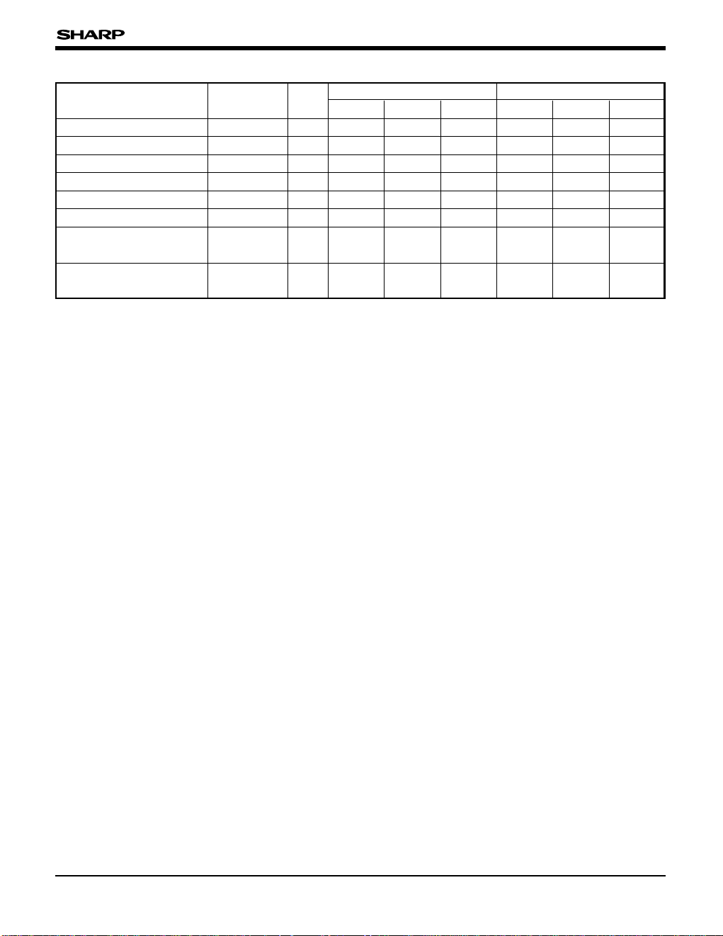
TA Operating Temperature 1
VCC1 VCC Supply Voltage (2.7 to 3.6 V) 2.7 3.6 V
VCC2 VCC Supply Voltage (3.3±0.3 V) 3.0 3.6 V
VCC3 VCC Supply Voltage (5.0±0.25 V) 4.75 5.25 V
VCC4 VCC Supply Voltage (5.0±0.5 V) 4.50 5.50 V
NOTE :
1. Test condition : Ambient temperature
PARAMETER NOTE MIN. MAX. UNIT VERSIONS
0
–40
+70
+85
- 22 -
C LH28F800BG-L
˚
˚C LH28F800BGH-L
LH28F800BG-L85/BGH-L85
Page 23

LH28F800BG-L/BGH-L (FOR TSOP, CSP)
TEST POINTSINPUT OUTPUT
1.35
1.35
2.7
0.0
1.5
1.5
3.0
0.0
TEST POINTSINPUT OUTPUT
2.0
0.8
2.0
0.8
2.4
0.45
TEST POINTSINPUT OUTPUT
6.2.1 CAPACITANCE
(NOTE 1)
TA = +25˚C, f = 1 MHz
SYMBOL PARAMETER TYP. MAX. UNIT CONDITION
CIN Input Capacitance 7 10 pF VIN = 0.0 V
COUT Output Capacitance 9 12 pF VOUT = 0.0 V
NOTE :
1. Sampled, not 100% tested.
6.2.2 AC INPUT/OUTPUT TEST CONDITIONS
AC test inputs are driven at 2.7 V for a Logic "1" and 0.0 V for a Logic "0". Input timing begins, and output
timing ends, at 1.35 V. Input rise and fall times (10% to 90%) < 10 ns.
Fig. 7 Transient Input/Output Reference Waveform for VCC = 2.7 to 3.6 V
AC test inputs are driven at 3.0 V for a Logic "1" and 0.0 V for a Logic "0". Input timing begins, and output
timing ends, at 1.5 V. Input rise and fall times (10% to 90%) < 10 ns.
Fig. 8 Transient Input/Output Reference Waveform for VCC = 3.3±0.3 V and
CC = 5.0±0.25 V (High Speed Testing Configuration)
V
AC test inputs are driven at VOH (2.4 VTTL) for a Logic "1" and VOL (0.45 VTTL) for a Logic "0". Input timing
begins at V
90%) < 10 ns.
IH (2.0 VTTL) and VIL (0.8 VTTL). Output timing ends at VIH and VIL. Input rise and fall times (10% to
Fig. 9 Transient Input/Output Reference Waveform for
V
CC = 5.0±0.5 V (Standard Testing Configuration)
- 23 -
Page 24
LH28F800BG-L/BGH-L (FOR TSOP, CSP)
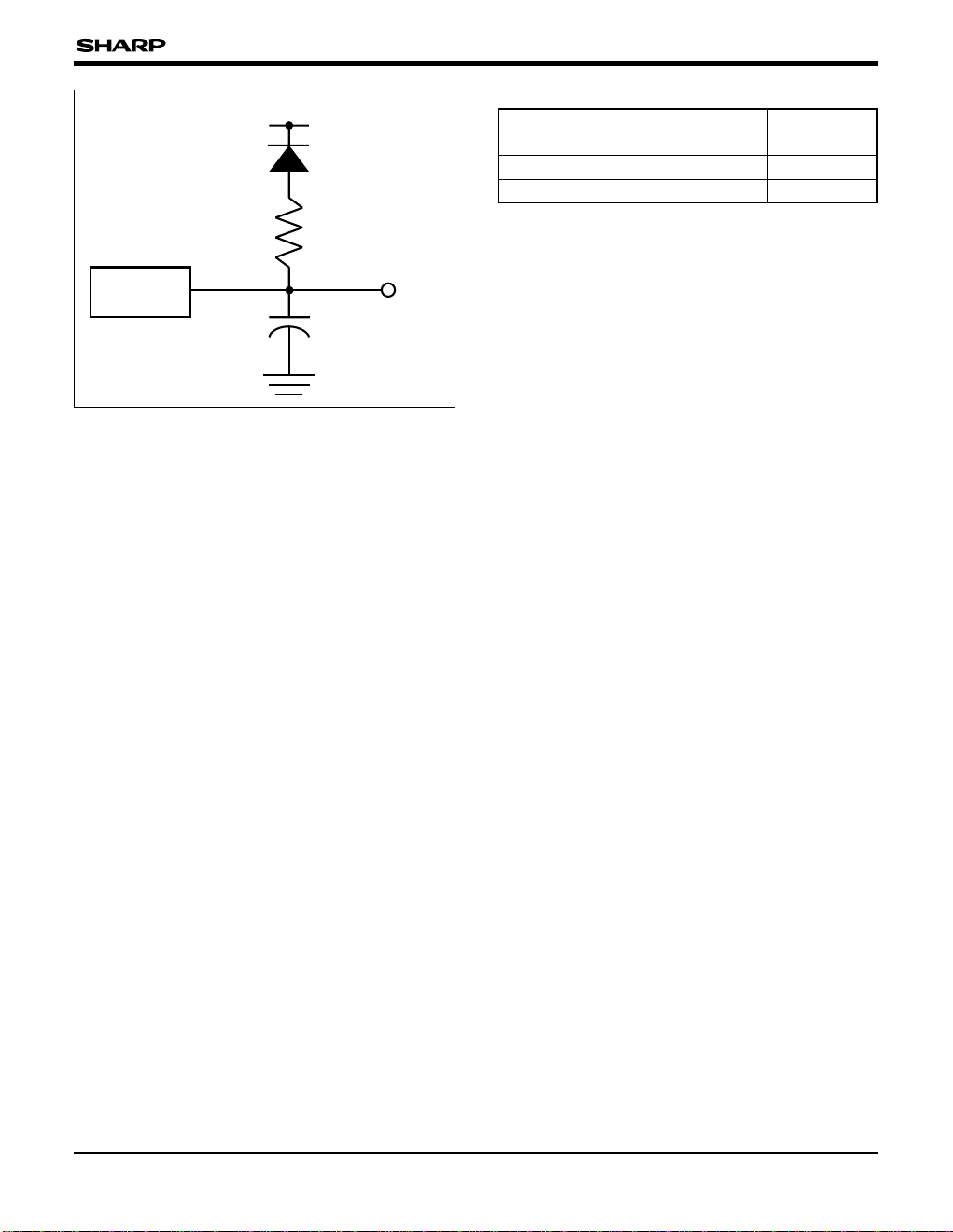
DEVICE
UNDER
TEST
C
L Includes Jig
Capacitance
RL = 3.3 kΩ
C
L
OUT
1.3 V
1N914
Test Configuration Capacitance Loading Value
TEST CONFIGURATION CL (pF)
VCC = 3.3±0.3 V, 2.7 to 3.6 V 50
VCC = 5.0±0.25 V
VCC = 5.0±0.5 V 100
NOTE :
1. Applied to high-speed products, LH28F800BG-L85 and
LH28F800BGH-L85.
(NOTE 1)
30
Fig. 10 Transient Equivalent Testing
Load Circuit
- 24 -
Page 25

LH28F800BG-L/BGH-L (FOR TSOP, CSP)
6.2.3 DC CHARACTERISTICS
SYMBOL
LI Input Load Current 1 ±0.5 ±1 µA
I
LO Output Leakage Current 1 ±0.5 ±10 µA
I
PARAMETER NOTE
VCC= 2.7 to 3.6 V
TYP. MAX. TYP. MAX.
25 50 30 100 µA V
ICCS VCC Standby Current 1, 3, 6
0.2 2 0.4 2 mA V
ICCD
VCCDeep PowerDown Current
LH28F800BG-L
LH28F800BGH-L
1
410 10µARP# = GND±0.2 V
420 20 IOUT (RY/BY#) = 0 mA
15 25 50 mA
ICCR VCC Read Current 1, 5, 6
517——mAVPP = 2.7 to 3.6 V
ICCW VCC Word Write Current 1, 7 5 17 35 mA VPP = 5.0±0.5 V
512 30mAVPP = 12.0±0.6 V
417——mAVPP = 2.7 to 3.6 V
ICCE VCC Block Erase Current 1, 7 4 17 30 mA VPP = 5.0±0.5 V
412 25mAVPP = 12.0±0.6 V
CCWS VCC Word Write or Block
I
ICCES Erase Suspend Current
IPPS
VPPStandby or Read Current
IPPR 10 200 10 200 µA VPP > VCC
VPP Deep Power-Down
IPPD
Current
1, 2 1 6 1 10 mA CE# = V
±2 ±15 ±2 ±15 µA V
1
1 0.1 5 0.1 5 µA RP# = GND±0.2 V
12 40 — — mA VPP = 2.7 to 3.6 V
IPPW VPP Word Write Current 1, 7 40 40 mA VPP = 5.0±0.5 V
825——mAVPP = 2.7 to 3.6 V
IPPE VPP Block Erase Current 1, 7 25 25 mA VPP = 5.0±0.5 V
PPWS VPP Word Write or Block
I
IPPES Erase Suspend Current
1 10 200 10 200 µA V
VCC = 5.0±0.5 V
UNIT
CC = VCC Max.
V
TEST
CONDITIONS
VIN = VCC or GND
CC = VCC Max.
V
VOUT = VCC or GND
CMOS Inputs
CC = VCC Max.
CE# = RP# = V
TTL Inputs
CC = VCC Max.
CE# = RP# = VIH
CMOS Inputs
CC = VCC Max.
V
CE# = GND
f = 5 MHz (3.3 V, 2.7 V),
8 MHz (5 V)
OUT = 0 mA
I
TTL Inputs
CC = VCC Max.
V
30 65 mA
CE# = GND
f = 5 MHz (3.3 V, 2.7 V),
8 MHz (5 V)
IOUT = 0 mA
IH
PP ≤ VCC
30 30 mA VPP = 12.0±0.6 V
20 20 mA VPP = 12.0±0.6 V
PP = VPPH1/2/3
CC±0.2 V
- 25 -
Page 26

LH28F800BG-L/BGH-L (FOR TSOP, CSP)
6.2.3 DC CHARACTERISTICS (contd.)
SYMBOL
PARAMETER NOTE
VIL Input Low Voltage 7
V
IH Input High Voltage 7 2.0
OL Output Low Voltage 3, 7 0.4 0.45 V IOL = 5.8 mA (5 V)
V
Output High Voltage
OH1
V
(TTL)
VCC= 2.7 to 3.6 V
MIN. MAX. MIN. MAX.
–
0.5 0.8
3, 7
2.4 2.4 V I
0.85 0.85
Output High Voltage
VOH2
(CMOS) V
VPP Lockout Voltage during
V
PPLK
Normal Operations
VPPVoltage during Word Write
V
PPH1
or Block Erase Operations
VPPVoltage during Word Write
VPPH2
or Block Erase Operations
VPPVoltage during Word Write
VPPH3
or Block Erase Operations
3, 7
4, 7 1.5 1.5 V
VCC VCC IOH = –2.5 mA
CC VCC
–
0.4
2.7 3.6
4.5 5.5 4.5 5.5 V
11.4 12.6 11.4 12.6 V
VLKO VCC Lockout Voltage 2.0 2.0 V
HH RP# Unlock Voltage 8, 9 11.4 12.6 11.4 12.6 V Unavailable WP#
V
NOTES :
1. All currents are in RMS unless otherwise noted. Typical
values at nominal V
currents are valid for all product versions (packages and
speeds).
2. I
CCWS and ICCES are specified with the device de-
selected. If reading or word writing in erase suspend
mode, the device’s current draw is the sum of I
I
CCES and ICCR or ICCW, respectively.
3. Includes RY/BY#.
4. Block erases and word writes are inhibited when V
PPLK, and not guaranteed in the range between VPPLK
V
(max.) and VPPH1 (min.), between VPPH1 (max.) and
V
PPH2 (min.), between VPPH2 (max.) and VPPH3 (min.),
and above V
CC voltage and TA = +25˚C. These
CCWS or
PP ≤
PPH3 (max.).
VCC = 5.0±0.5 V
–
0.5 0.8 V
CC
V
+0.5 +0.5
2.0
–
0.4 I
——
5. Automatic Power Saving (APS) reduces typical I
1 mA at 5 V V
static operation.
6. CMOS inputs are either V
inputs are either V
7. Sampled, not 100% tested.
8. Boot block erases and word writes are inhibited when
the corresponding RP# = V
and word write operations are not guaranteed with V
RP# < V
HH and should not be attempted.
9. RP# connection to a V
maximum cumulative period of 80 hours.
UNIT
CC
V
V
CC = VCC Min.
V
I
OL
CC = VCC Min.
V
OH =
I
OH
VCC = VCC Min.
V
CC = VCC Min.
V
V
OH =
V
CC and 3 mA at 2.7 V and 3.3 V VCC in
CC±0.2 V or GND±0.2 V. TTL
IL or VIH.
IH or WP# = VIL. Block erase
HH supply is allowed for a
TEST
CONDITIONS
= 2.0 mA (3.3 V, 2.7 V)
–
2.5 mA (5 V)
= –2.0 mA
–
100 µA
(3.3 V, 2.7 V)
CCR to
IH <
- 26 -
Page 27

LH28F800BG-L/BGH-L (FOR TSOP, CSP)
6.2.4 AC CHARACTERISTICS - READ-ONLY OPERATIONS
• VCC = 2.7 to 3.6 V, TA = 0 to +70˚C or –40 to +85˚C
VERSIONS
SYMBOL
PARAMETER NOTE MIN. MAX. MIN. MAX.
(NOTE 1)
LH28F800BG-L85 LH28F800BG-L12
LH28F800BGH-L85 LH28F800BGH-L12
tAVAV Read Cycle Time 120 150 ns
tAVQV Address to Output Delay 120 150 ns
tELQV CE# to Output Delay 2 120 150 ns
tPHQV RP# High to Output Delay 600 600 ns
tGLQV OE# to Output Delay 2 50 55 ns
tELQX CE# to Output in Low Z 3 0 0 ns
tEHQZ CE# High to Output in High Z 3 55 55 ns
tGLQX OE# to Output in Low Z 3 0 0 ns
tGHQZ OE# High to Output in High Z 3 20 25 ns
t
OH
Output Hold from Address, CE# or
OE# Change, Whichever Occurs First
30 0 ns
•VCC = 3.3±0.3 V, TA = 0 to +70˚C or –40 to +85˚C
LH28F800BG-L85 LH28F800BG-L12
LH28F800BGH-L85 LH28F800BGH-L12
SYMBOL
VERSIONS
PARAMETER NOTE MIN. MAX. MIN. MAX.
tAVAV Read Cycle Time 100 130 ns
tAVQV Address to Output Delay 100 130 ns
tELQV CE# to Output Delay 2 100 130 ns
tPHQV RP# High to Output Delay 600 600 ns
tGLQV OE# to Output Delay 2 50 55 ns
tELQX CE# to Output in Low Z 3 0 0 ns
tEHQZ CE# High to Output in High Z 3 55 55 ns
tGLQX OE# to Output in Low Z 3 0 0 ns
tGHQZ OE# High to Output in High Z 3 20 25 ns
t
OH
Output Hold from Address, CE# or
OE# Change, Whichever Occurs First
30 0 ns
NOTES :
1. See AC Input/Output Reference Waveform (Fig. 7 through Fig. 9) for maximum allowable input slew rate.
2. OE# may be delayed up to t
3. Sampled, not 100% tested.
ELQV-tGLQV after the falling edge of CE# without impact on tELQV.
UNIT
UNIT
- 27 -
Page 28

LH28F800BG-L/BGH-L (FOR TSOP, CSP)
6.2.4 AC CHARACTERISTICS - READ-ONLY OPERATIONS (contd.)
(NOTE 1)
•VCC = 5.0±0.25 V, 5.0±0.5 V, TA = 0 to +70˚C or –40 to +85˚C
(NOTE 4)
LH28F800BG-L85
LH28F800BGH-L85
(NOTE 5)
LH28F800BG-L85
LH28F800BGH-L85
(NOTE 5)
LH28F800BG-L12
LH28F800BGH-L12
UNIT
SYMBOL
VCC±0.25 V
VERSIONS
VCC±0.5 V
PARAMETER NOTE MIN. MAX. MIN. MAX. MIN. MAX.
tAVAV Read Cycle Time 85 90 120 ns
tAVQV Address to Output Delay 85 90 120 ns
tELQV CE# to Output Delay 2 85 90 120 ns
tPHQV RP# High to Output Delay 400 400 400 ns
tGLQV OE# to Output Delay 2 40 45 50 ns
tELQX CE# to Output in Low Z 3 0 0 0 ns
tEHQZ CE# High to Output in High Z 3 55 55 55 ns
tGLQX OE# to Output in Low Z 3 0 0 0 ns
tGHQZ OE# High to Output in High Z 3 10 10 15 ns
Output Hold from Address,
OH CE# or OE# Change, 3 0 0 0 ns
t
Whichever Occurs First
NOTES :
1. See AC Input/Output Reference Waveform (Fig. 7
through Fig. 9) for maximum allowable input slew rate.
2. OE# may be delayed up to t
edge of CE# without impact on t
3. Sampled, not 100% tested.
4. See Fig. 8 "Transient Input/Output Reference
Waveform" and Fig. 10 "Transient Equivalent Testing
Load Circuit" (High Speed Configuration) for testing
characteristics.
ELQV-tGLQV after the falling
ELQV.
5. See Fig. 9 "Transient Input/Output Reference
Waveform" and Fig. 10 "Transient Equivalent Testing
Load Circuit" (Standard Configuration) for testing
characteristics.
- 28 -
Page 29

LH28F800BG-L/BGH-L (FOR TSOP, CSP)
ADDRESSES (A)
CE# (E)
OE# (G)
WE# (W)
DATA (D/Q)
(DQ
0-DQ15)
RP# (P)
V
CC
Standby
Device
Address Selection
Data Valid
Address Stable
t
AVAV
tEHQZ
tGHQZ
High Z
Valid Output
t
GLQV
tELQV
tGLQX
tELQX
tAVQV
tPHQV
High Z
t
OH
VIL
VOH
VOL
VIH
VIH
VIH
VIH
VIH
VIL
VIL
VIL
VIL
Fig. 11 AC Waveform for Read Operations
- 29 -
Page 30

LH28F800BG-L/BGH-L (FOR TSOP, CSP)
6.2.5 AC CHARACTERISTICS - WRITE OPERATIONS
• VCC = 2.7 to 3.6 V, TA = 0 to +70˚C or –40 to +85˚C
VERSIONS
SYMBOL
PARAMETER NOTE MIN. MAX. MIN. MAX.
(NOTE 1)
LH28F800BG-L85 LH28F800BG-L12
LH28F800BGH-L85 LH28F800BGH-L12
tAVAV Write Cycle Time 120 150 ns
tPHWL RP# High Recovery to WE# Going Low 2 1 1 µs
tELWL CE# Setup to WE# Going Low 10 10 ns
tWLWH WE# Pulse Width 50 50 ns
tPHHWH RP# VHH Setup to WE# Going High 2 100 100 ns
tSHWH WP# VIH Setup to WE# Going High 2 100 100 ns
tVPWH VPP Setup to WE# Going High 2 100 100 ns
tAVWH Address Setup to WE# Going High 3 50 50 ns
tDVWH Data Setup to WE# Going High 3 50 50 ns
tWHDX Data Hold from WE# High 5 5 ns
tWHAX Address Hold from WE# High 5 5 ns
tWHEH CE# Hold from WE# High 10 10 ns
tWHWL WE# Pulse Width High 30 30 ns
tWHRL WE# High to RY/BY# Going Low 100 100 ns
tWHGL Write Recovery before Read 0 0 ns
tQVVL VPP Hold from Valid SRD, RY/BY# High 2, 4 0 0 ns
tQVPH RP# VHH Hold from Valid SRD, RY/BY# High 2, 4 0 0 ns
tQVSL WP# VIH Hold from Valid SRD, RY/BY# High 2, 4 0 0 ns
NOTES :
PP should be held at VPPH1/2/3 (and if necessary RP#
1. Read timing characteristics during block erase and word
write operations are the same as during read-only
operations. Refer to Section 6.2.4 "AC CHARAC-
TERISTICS" for read-only operations.
2. Sampled, not 100% tested.
3. Refer to Table 3 for valid A
word write.
IN and DIN for block erase or
4. V
should be held at V
or word write success (SR.1/3/4/5 = 0 : on Boot Blocks,
SR.3/4/5 = 0 : on Parameter Blocks and Main Blocks).
HH) until determination of block erase
UNIT
- 30 -
Page 31

LH28F800BG-L/BGH-L (FOR TSOP, CSP)
6.2.5 AC CHARACTERISTICS - WRITE OPERATIONS (contd.)
(NOTE 1)
•VCC = 3.3±0.3 V, TA = 0 to +70˚C or –40 to +85˚C
LH28F800BG-L85 LH28F800BG-L12
LH28F800BGH-L85 LH28F800BGH-L12 UNIT
SYMBOL
VERSIONS
PARAMETER NOTE MIN. MAX. MIN. MAX.
tAVAV Write Cycle Time 100 130 ns
tPHWL RP# High Recovery to WE# Going Low 2 1 1 µs
tELWL CE# Setup to WE# Going Low 10 10 ns
tWLWH WE# Pulse Width 50 50 ns
tPHHWH RP# VHH Setup to WE# Going High 2 100 100 ns
tSHWH WP# VIH Setup to WE# Going High 2 100 100 ns
tVPWH VPP Setup to WE# Going High 2 100 100 ns
tAVWH Address Setup to WE# Going High 3 50 50 ns
tDVWH Data Setup to WE# Going High 3 50 50 ns
tWHDX Data Hold from WE# High 5 5 ns
tWHAX Address Hold from WE# High 5 5 ns
tWHEH CE# Hold from WE# High 10 10 ns
tWHWL WE# Pulse Width High 30 30 ns
tWHRL WE# High to RY/BY# Going Low 100 100 ns
tWHGL Write Recovery before Read 0 0 ns
tQVVL VPP Hold from Valid SRD, RY/BY# High 2, 4 0 0 ns
tQVPH RP# VHH Hold from Valid SRD, RY/BY# High 2, 4 0 0 ns
tQVSL WP# VIH Hold from Valid SRD, RY/BY# High 2, 4 0 0 ns
NOTES :
PP should be held at VPPH1/2/3 (and if necessary RP#
1. Read timing characteristics during block erase and word
write operations are the same as during read-only
operations. Refer to Section 6.2.4 "AC CHARAC-
TERISTICS" for read-only operations.
2. Sampled, not 100% tested.
3. Refer to Table 3 for valid A
word write.
IN and DIN for block erase or
4. V
should be held at V
or word write success (SR.1/3/4/5 = 0 : on Boot Blocks,
SR.3/4/5 = 0 : on Parameter Blocks and Main Blocks).
HH) until determination of block erase
- 31 -
Page 32

LH28F800BG-L/BGH-L (FOR TSOP, CSP)
6.2.5 AC CHARACTERISTICS - WRITE OPERATIONS (contd.)
(NOTE 1)
•VCC = 5.0±0.25 V, 5.0±0.5 V, TA = 0 to +70˚C or –40 to +85˚C
(NOTE 5)
LH28F800BG-L85
LH28F800BGH-L85
(NOTE 6)
LH28F800BG-L85
LH28F800BGH-L85
(NOTE 6)
LH28F800BG-L12
LH28F800BGH-L12
SYMBOL
VCC±0.25 V
VERSIONS
VCC±0.5 V
PARAMETER NOTE MIN. MAX. MIN. MAX. MIN. MAX.
tAVAV Write Cycle Time 85 90 120 ns
PHWL
t
RP# High Recovery to WE#
Going Low
2111µs
tELWL CE# Setup to WE# Going Low 10 10 10 ns
tWLWH WE# Pulse Width 40 40 40 ns
tPHHWH
tSHWH
RP# VHHSetup to WE# Going High
WP# VIHSetup to WE# Going High
2 100 100 100 ns
2 100 100 100 ns
tVPWH VPP Setup to WE# Going High 2 100 100 100 ns
tAVWH
Address Setup to WE# Going High
3404040ns
tDVWH Data Setup to WE# Going High 3 40 40 40 ns
tWHDX Data Hold from WE# High 5 5 5 ns
tWHAX Address Hold from WE# High 5 5 5 ns
tWHEH CE# Hold from WE# High 10 10 10 ns
tWHWL WE# Pulse Width High 30 30 30 ns
tWHRL
WE# High to RY/BY# Going Low
90 90 90 ns
tWHGL Write Recovery before Read 0 0 0 ns
QVVL
t
QVPH
t
QVSL
t
VPP Hold from Valid SRD,
RY/BY# High
RP# VHH Hold from Valid SRD,
RY/BY# High
WP# VIH Hold from Valid SRD,
RY/BY# High
2, 4 0 0 0 ns
2, 4 0 0 0 ns
2, 4 0 0 0 ns
NOTES :
1. Read timing characteristics during block erase and word
write operations are the same as during read-only
operations. Refer to Section 6.2.4 "AC CHARAC-
TERISTICS" for read-only operations.
2. Sampled, not 100% tested.
3. Refer to Table 3 for valid A
word write.
4. V
PP should be held at VPPH1/2/3 (and if necessary RP#
should be held at V
or word write success (SR.1/3/4/5 = 0 : on Boot Blocks,
SR.3/4/5 = 0 : on Parameter Blocks and Main Blocks).
IN and DIN for block erase or
HH) until determination of block erase
5. See Fig. 8 "Transient Input/Output Reference
Waveform" and Fig. 10 "Transient Equivalent Testing
Load Circuit" (High Seed Configuration) for testing
characteristics.
6. See Fig. 9 "Transient Input/Output Reference
Waveform" and Fig. 10 "Transient Equivalent Testing
Load Circuit" (Standard Configuration) for testing
characteristics.
UNIT
- 32 -
Page 33

(NOTE 1) (NOTE 2) (NOTE 3) (NOTE 4) (NOTE 5) (NOTE 6)
VIL
VIH
VOH
VIH
VIH
VIH
VIL
VIL
VIL
VOL
VIL
VIH
VHH
VIL
VPPLK
VPPH1/2/3
VIH
VIL
ADDRESSES (A)
CE# (E)
OE# (G)
WE# (W)
DATA (D/Q)
RP# (P)
VPP (V)
RY/BY# (R)
A
IN AIN
tAVAV tAVWH
tELWL
tWHEH
tWHGL
tWHWL tWHQV1/2/3/4
tWLWH
tDVWH
tWHDX
Valid
SRD
t
PHWL
tWHRL
tVPWH
tQVVL
DIN
DIN
High Z
DIN
WP# (S)
VIH
VIL
tPHHWH
tQVPH
tSHWH
tQVSL
tWHAX
NOTES :
1. VCC power-up and standby.
2. Write block erase or word write setup.
3. Write block erase confirm or valid address and data.
4. Automated erase or program delay.
5. Read status register data.
6. Write Read Array command.
Fig. 12 AC Waveform for WE#-Controlled Write Operations
LH28F800BG-L/BGH-L (FOR TSOP, CSP)
- 33 -
Page 34

LH28F800BG-L/BGH-L (FOR TSOP, CSP)
6.2.6 ALTERNATIVE CE#-CONTROLLED WRITES
(NOTE 1)
•VCC = 2.7 to 3.6 V, TA = 0 to +70˚C or – 40 to +85˚C
LH28F800BG-L85 LH28F800BG-L12
LH28F800BGH-L85 LH28F800BGH-L12 UNIT
SYMBOL
t
AVAV
t
PHEL
t
WLEL
t
ELEH
VERSIONS
PARAMETER NOTE MIN. MAX. MIN. MAX.
Write Cycle Time 120 150 ns
RP# High Recovery to CE# Going Low 2 1 1 µs
WE# Setup to CE# Going Low 0 0 ns
CE# Pulse Width 70 70 ns
tPHHEH RP# VHH Setup to CE# Going High 2 100 100 ns
tSHEH WP# VIH Setup to CE# Going High 2 100 100 ns
tVPEH VPP Setup to CE# Going High 2 100 100 ns
tAVEH Address Setup to CE# Going High 3 50 50 ns
tDVEH Data Setup to CE# Going High 3 50 50 ns
tEHDX Data Hold from CE# High 5 5 ns
tEHAX Address Hold from CE# High 5 5 ns
tEHWH WE# Hold from CE# High 0 0 ns
tEHEL CE# Pulse Width High 25 25 ns
tEHRL CE# High to RY/BY# Going Low 100 100 ns
tEHGL Write Recovery before Read 0 0 ns
tQVVL VPP Hold from Valid SRD, RY/BY# High 2, 4 0 0 ns
tQVPH RP# VHH Hold from Valid SRD, RY/BY# High 2, 4 0 0 ns
tQVSL WP# VIH Hold from Valid SRD, RY/BY# High 2, 4 0 0 ns
NOTES :
PP should be held at VPPH1/2/3 (and if necessary RP#
1. In systems where CE# defines the write pulse width
(within a longer WE# timing waveform), all setup, hold,
and inactive WE# times should be measured relative to
the CE# waveform.
2. Sampled, not 100% tested.
3. Refer to Table 3 for valid A
word write.
IN and DIN for block erase or
4. V
should be held at V
or word write success (SR.1/3/4/5 = 0 : on Boot Blocks,
SR.3/4/5 = 0 : on Parameter Blocks and Main Blocks).
HH) until determination of block erase
- 34 -
Page 35
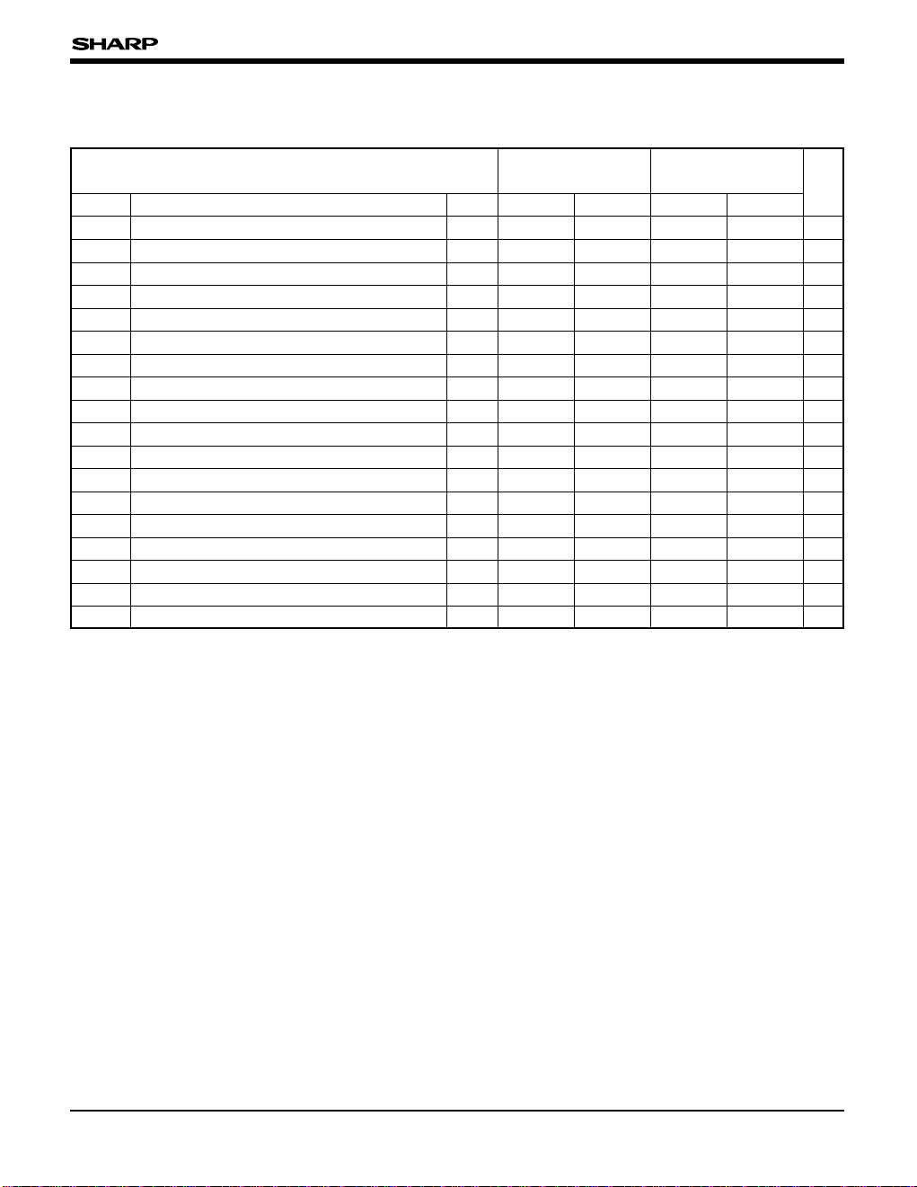
LH28F800BG-L/BGH-L (FOR TSOP, CSP)
6.2.6 ALTERNATIVE CE#-CONTROLLED WRITES (contd.)
(NOTE 1)
•VCC = 3.3±0.3 V, TA = 0 to +70˚C or –40 to +85˚C
LH28F800BG-L85 LH28F800BG-L12
LH28F800BGH-L85 LH28F800BGH-L12
SYMBOL
t
AVAV
t
PHEL
t
WLEL
t
ELEH
t
PHHEH
VERSIONS
PARAMETER NOTE MIN. MAX. MIN. MAX.
Write Cycle Time 100 130 ns
RP# High Recovery to CE# Going Low 2 1 1 µs
WE# Setup to CE# Going Low 0 0 ns
CE# Pulse Width 70 70 ns
RP# VHHSetup to CE# Going High 2 100 100 ns
tSHEH WP# VIH Setup to CE# Going High 2 100 100 ns
tVPEH VPP Setup to CE# Going High 2 100 100 ns
tAVEH Address Setup to CE# Going High 3 50 50 ns
tDVEH Data Setup to CE# Going High 3 50 50 ns
tEHDX Data Hold from CE# High 5 5 ns
tEHAX Address Hold from CE# High 5 5 ns
tEHWH WE# Hold from CE# High 0 0 ns
tEHEL CE# Pulse Width High 25 25 ns
tEHRL CE# High to RY/BY# Going Low 100 100 ns
tEHGL Write Recovery before Read 0 0 ns
tQVVL VPP Hold from Valid SRD, RY/BY# High 2, 4 0 0 ns
tQVPH RP# VHH Hold from Valid SRD, RY/BY# High 2, 4 0 0 ns
tQVSL WP# VIH Hold from Valid SRD, RY/BY# High 2, 4 0 0 ns
NOTES :
PP should be held at VPPH1/2/3 (and if necessary RP#
1. In systems where CE# defines the write pulse width
(within a longer WE# timing waveform), all setup, hold,
and inactive WE# times should be measured relative to
the CE# waveform.
2. Sampled, not 100% tested.
3. Refer to Table 3 for valid A
word write.
IN and DIN for block erase or
4. V
should be held at V
or word write success (SR.1/3/4/5 = 0 : on Boot Blocks,
SR.3/4/5 = 0 : on Parameter Blocks and Main Blocks).
HH) until determination of block erase
UNIT
- 35 -
Page 36
LH28F800BG-L/BGH-L (FOR TSOP, CSP)
6.2.6 ALTERNATIVE CE#-CONTROLLED WRITES (contd.)
(NOTE 1)
•VCC = 5.0±0.25 V, 5.0±0.5 V, TA = 0 to +70˚C or –40 to +85˚C
(NOTE 5)
LH28F800BG-L85
LH28F800BGH-L85
(NOTE 6)
LH28F800BG-L85
LH28F800BGH-L85
(NOTE 6)
LH28F800BG-L12
LH28F800BGH-L12
UNIT
2111µs
2 100 100 100 ns
2 100 100 100 ns
SYMBOL
t
AVAV
PHEL
t
t
WLEL
t
ELEH
t
PHHEH
tSHEH
VCC±0.25 V
VERSIONS
VCC±0.5 V
PARAMETER NOTE MIN. MAX. MIN. MAX. MIN. MAX.
Write Cycle Time 85 90 120 ns
RP# High Recovery to CE#
Going Low
WE# Setup to CE# Going Low 0 0 0 ns
CE# Pulse Width 50 50 50 ns
RP# VHHSetup to CE# Going High
WP# VIHSetup to CE# Going High
tVPEH VPP Setup to CE# Going High 2 100 100 100 ns
tAVEH
Address Setup to CE# Going High
3404040ns
tDVEH Data Setup to CE# Going High 3 40 40 40 ns
tEHDX Data Hold from CE# High 5 5 5 ns
tEHAX Address Hold from CE# High 5 5 5 ns
tEHWH WE# Hold from CE# High 0 0 0 ns
tEHEL CE# Pulse Width High 25 25 25 ns
tEHRL CE# High to RY/BY# Going Low 90 90 90 ns
tEHGL Write Recovery before Read 0 0 0 ns
t
QVVL
QVPH
t
t
QVSL
VPP Hold from Valid SRD,
RY/BY# High
RP# VHH Hold from Valid SRD,
RY/BY# High
WP# VIH Hold from Valid SRD,
RY/BY# High
2, 4 0 0 0 ns
2, 4 0 0 0 ns
2, 4 0 0 0 ns
NOTES :
1. In systems where CE# defines the write pulse width
(within a longer WE# timing waveform), all setup, hold,
and inactive WE# times should be measured relative to
the CE# waveform.
2. Sampled, not 100% tested.
3. Refer to Table 3 for valid A
word write.
4. V
PP should be held at VPPH1/2/3 (and if necessary RP#
should be held at V
or word write success (SR.1/3/4/5 = 0 : on Boot Blocks,
SR.3/4/5 = 0 : on Parameter Blocks and Main Blocks).
IN and DIN for block erase or
HH) until determination of block erase
5. See Fig. 8 "Transient Input/Output Reference
Waveform" and Fig. 10 "Transient Equivalent Testing
Load Circuit" (High Seed Configuration) for testing
characteristics.
6. See Fig. 9 "Transient Input/Output Reference
Waveform" and Fig. 10 "Transient Equivalent Testing
Load Circuit" (Standard Configuration) for testing
characteristics.
- 36 -
Page 37

VIL
VIH
VIH
VIH
VIH
VIL
VIL
VIL
VOL
VOH
VIL
VIH
VHH
VIL
VPPLK
VPPH1/2/3
VIH
VIL
ADDRESSES (A)
WE# (W)
OE# (G)
CE# (E)
DATA (D/Q)
RP# (P)
VPP (V)
RY/BY# (R)
WP# (S)
V
IH
VIL
AIN AIN
tAVAV tAVEH
tWLEL
tEHWH
tEHGL
tEHEL tEHQV1/2/3/4
Valid
SRD
t
PHEL
tEHRL
tVPEH
tQVVL
DIN
DIN
High Z
DIN
tPHHEH
tQVPH
tSHEH
tEHAX
tELEH
tDVEH
tEHDX
tQVSL
(NOTE 1) (NOTE 2) (NOTE 3) (NOTE 4) (NOTE 5) (NOTE 6)
NOTES :
1. VCC power-up and standby.
2. Write block erase or word write setup.
3. Write block erase confirm or valid address and data.
4. Automated erase or program delay.
5. Read status register data.
6. Write Read Array command.
Fig. 13 AC Waveform for CE#-Controlled Write Operations
LH28F800BG-L/BGH-L (FOR TSOP, CSP)
- 37 -
Page 38

6.2.7 RESET OPERATIONS
RP# (P)
V
IL
VIH
VOH
VIH
VOH
VOL
VIL
VOL
RY/BY# (R)
RY/BY# (R)
RP# (P)
VIL
(C) RP# Rising Timing
V
IH
2.7 V/3.3 V/5 V
VIL
RP# (P)
V
CC
(A) Reset During Read Array Mode
(B) Reset During Block Erase or Word Write
tPLPH
tPLRH
tPLPH
t235VPH
LH28F800BG-L/BGH-L (FOR TSOP, CSP)
SYMBOL
NOTES :
1. These specifications are valid for all product versions
t
PLPH
RP# Pulse Low Time
(If RP# is tied to VCC, this 100 100 100 ns
specification is not applicable)
RP# Low to Reset during
t
PLRH
t
235VPHVCC
Block Erase or Word Write
V
2.7 V to RP# High
CC
3.0 V to RP# High 4 100 100 100 ns
4.5 V to RP# High
V
CC
(packages and speeds).
PARAMETER NOTE
Fig. 14 AC Waveform for Reset Operation
Reset AC Specifications
2, 3 22 20 12 µs
2. If RP# is asserted while a block erase or word write
operation is not executing, the reset will complete within
100 ns.
(NOTE 1)
VCC = 2.7 to 3.6 V VCC = 3.3±0.3 V VCC = 5.0±0.5 V
MIN. MAX. MIN. MAX. MIN. MAX.
3. A reset time, t
or RP# going high until outputs are valid.
4. When the device power-up, holding RP#-low minimum
100 ns is required after V
range and also has been in stable there.
PHQV, is required from the latter of RY/BY#
CC has been in predefined
- 38 -
UNIT
Page 39
LH28F800BG-L/BGH-L (FOR TSOP, CSP)
6.2.8 BLOCK ERASE AND WORD WRITE PERFORMANCE
•VCC = 2.7 to 3.6 V, TA = 0 to +70˚C or –40 to +85˚C
SYMBOL
PARAMETER NOTE
32 k-Word
tWHQV1 Word Write
Block
tEHQV1 Time 4 k-Word
Block
32 k-Word
Block Write
Block
Time 4 k-Word
Block
32 k-Word
tWHQV2
tEHQV2
Block Erase Block
Time
4 k-Word
Block
t
WHRH1 Word Write Suspend
tEHRH1 Latency Time to Read
t
WHRH2
t
EHRH2
Erase Suspend Latency
Time to Read
•VCC = 3.3±0.3 V, TA = 0 to +70˚C or –40 to +85˚C
SYMBOL
PARAMETER NOTE
32 k-Word
tWHQV1 Word Write
Block
tEHQV1 Time 4 k-Word
Block
32 k-Word
Block Write
Block
Time 4 k-Word
Block
32 k-Word
tWHQV2
tEHQV2
Block Erase Block
Time
4 k-Word
Block
t
WHRH1 Word Write Suspend
tEHRH1 Latency Time to Read
t
WHRH2
t
EHRH2
Erase Suspend Latency
Time to Read
NOTES :
1. Typical values measured at TA = +25˚C and nominal
voltages. Subject to change based on device
characterization.
2. Excludes system-level overhead.
VPP = 2.7 to 3.6 V VPP = 5.0±0.5 V VPP = 12.0±0.6 V
TYP.
(NOTE 1)
MAX. MIN.
MIN.
2 44.6 17.7 12.6 µs
2 45.9 26.1 24.5 µs
2 1.46 0.58 0.42 s
2 0.19 0.11 0.11 s
2 1.14 0.61 0.51 s
2 0.38 0.32 0.31 s
78 68 67µs
18 22 11 14 11 14 µs
VPP = 3.3±0.3 V VPP = 5.0±0.5 V VPP = 12.0±0.6 V
TYP.
(NOTE 1)
MAX. MIN.
MIN.
2 44 17.3 12.3 µs
2 45 25.6 24 µs
2 1.44 0.57 0.41 s
2 0.19 0.11 0.1 s
2 1.11 0.59 0.5 s
2 0.37 0.31 0.3 s
67 57 56µs
16.2 20 9.6 12 9.6 12 µs
3. These performance numbers are valid for all speed
versions.
4. Sampled, not 100% tested.
(NOTE 3, 4)
(NOTE 1)
TYP.
(NOTE 1)
TYP.
MAX. MIN.
MAX. MIN.
(NOTE 1)
TYP.
(NOTE 1)
TYP.
MAX.
MAX.
UNIT
UNIT
- 39 -
Page 40
LH28F800BG-L/BGH-L (FOR TSOP, CSP)
6.2.8 BLOCK ERASE AND WORD WRITE PERFORMANCE (contd.)
(NOTE 3, 4)
•VCC = 5.0 V±0.25 V, 5.0±0.5 V, TA = 0 to +70˚C or –40 to +85˚C
SYMBOL
tWHQV1
tEHQV1 4 k-Word Block 2 18.3 17 µs
Word Write Time
Block Write Time
tWHQV2
tEHQV2 4 k-Word Block 2 0.26 0.25 s
tWHRH1
tEHRH1
tWHRH2
EHRH2
t
Block Erase Time
Word Write Suspend Latency Time to Read 5 6 4 5 µs
Erase Suspend Latency Time to Read 9.6 12 9.6 12 µs
PARAMETER NOTE
32 k-Word Block 2 12.2 8.4 µs
32 k-Word Block 2 0.4 0.28 s
4 k-Word Block 2 0.08 0.07 s
32 k-Word Block 2 0.46 0.39 s
VPP = 5.0±0.5 V VPP = 12.0±0.6 V
MIN.
TYP.
(NOTE 1)
MAX. MIN.
TYP.
(NOTE 1)
MAX.
NOTES :
1. Typical values measured at TA = +25˚C and nominal
voltages. Subject to change based on device
characterization.
2. Excludes system-level overhead.
3. These performance numbers are valid for all speed
versions.
4. Sampled, not 100% tested.
UNIT
- 40 -
Page 41
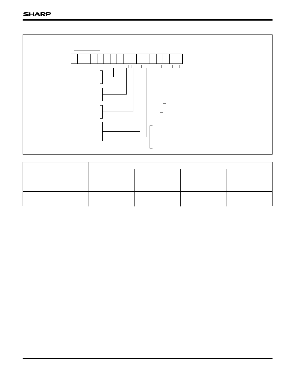
7 ORDERING INFORMATION
LH28F800BG
(H)
ET-L85
Device Density
800 = 8 M-bit
Access Speed (ns)
85 : 85 ns (5.0±0.25 V), 90 ns (5.0±0.5 V)
100 ns (3.3±0.3 V), 120 ns (2.7 to 3.6 V)
12 : 120 ns (5.0±0.5 V), 130 ns (3.3±0.3 V),
150 ns (2.7 to 3.6 V)
Package
E = 48-pin TSOP (I) (TSOP048-P-1220) Normal bend
R = 48-pin TSOP (I) (TSOP048-P-1220) Reverse bend
B = 48-ball CSP (FBGA048-P-0808)
Architecture
B = Boot Block
Power Supply Type
G = SmartVoltage Technology
Operating Temperature
Blank = 0 to +70°C
H = –40 to +85°C
Product line designator for all SHARP Flash products
Block Locate Option
T = Top Boot
B = Bottom Boot
OPTION ORDER CODE
1
LH28F800BGXX-XL85
LH28F800BGXX-XL12
2
VCC= 2.7 to 3.6 V VCC= 3.3±0.3 V VCC= 5.0±0.5 V VCC= 5.0±0.25 V
50 pF load, 50 pF load, 100 pF load, 30 pF load,
1.35 V I/O Levels 1.5 V I/O Levels TTL I/O Levels 1.5 V I/O Levels
120 ns 100 ns 90 ns 85 ns
150 ns 130 ns 120 ns
LH28F800BG-L/BGH-L (FOR TSOP, CSP)
VALID OPERATIONAL COMBINATIONS
- 41 -
Page 42

1.2
0.1
±0.2
±0.05
±0.1
MAX.
±0.2
TYP.
25
48
24
1
12.0
48
_
0.2
0.5
0.1
0.10
±0.08
20.0
±0.3
18.4
0.125
M
0.125
19.0
±0.1
1.0
±0.1
Package base plane
48 TSOP (TSOP048-P-1220)
PACKAGING
Page 43
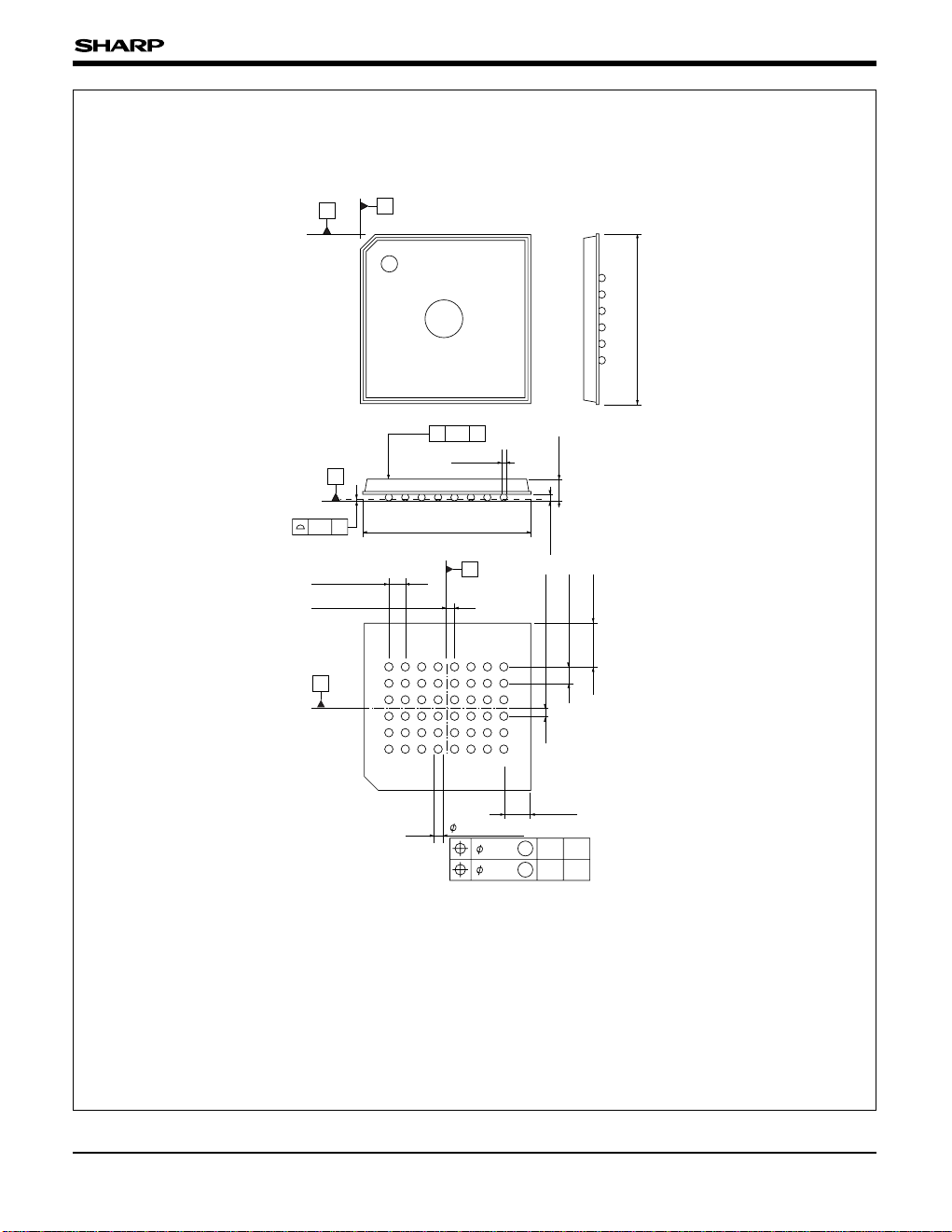
S
M
0.30 AB
SCD
M
0.15
A
B
S
8.0
+
0.2
1.2
MAX.
0.35
±0.05
0.1 S
0.1 S
∗
0.4
TYP.
0
C
D
0.45
±0.03
0.8
TYP.
0.4
TYP.
2.0
TYP.
0.8
TYP.
0.4
TYP.
1.2
TYP.
F
A
1
8
∗Land hole diameter
for ball mounting
8.0
0
+
0.2
/ /
48 CSP (FBGA048-P-0808)
PACKAGING
 Loading...