

Datasheet LH28F160S5H-L10, LH28F160S5-L70, LH28F160S5H-L70, LH28F160S5-L10 Datasheet (Sharp)
Page 1

LH28F160S5-L/S5H-L
DESCRIPTION
The LH28F160S5-L/S5H-L flash memories with
Smart 5 technology are high-density, low-cost,
nonvolatile, read/write storage solution for a wide
range of applications, having high programming
performance is achieved through highly-optimized
page buffer operations. Their symmetrically-blocked
architecture, flexible voltage and enhanced cycling
capability provide for highly flexible component
suitable for resident flash arrays, SIMMs and
memory cards. Their enhanced suspend
capabilities provide for an ideal solution for code +
data storage applications. For secure code storage
applications, such as networking, where code is
either directly executed out of flash or downloaded
to DRAM, the LH28F160S5-L/S5H-L offer three
levels of protection : absolute protection with V
PP at
GND, selective hardware block locking, or flexible
software block locking. These alternatives give
designers ultimate control of their code security
needs. The LH28F160S5-L/S5H-L are conformed
to the flash Scalable Command Set (SCS) and the
Common Flash Interface (CFI) specification which
enable universal and upgradable interface, enable
the highest system/device data transfer rates and
minimize device and system-level implementation
costs.
FEATURES
• Smart 5 technology
–5 V V
CC
–5 V VPP
• High speed write performance
– Two 32-byte page buffers
– 2 µs/byte write transfer rate
• Common Flash Interface (CFI)
– Universal & upgradable interface
• Scalable Command Set (SCS)
• High performance read access time
LH28F160S5-L70
– 70 ns (5.0±0.25 V)/80 ns (5.0±0.5 V)
LH28F160S5H-L70
– 70 ns (5.0±0.25 V)/90 ns (5.0±0.5 V)
LH28F160S5-L10/S5H-L10
– 100 ns (5.0±0.5 V)
• Enhanced automated suspend options
– Write suspend to read
– Block erase suspend to write
– Block erase suspend to read
• Enhanced data protection features
– Absolute protection with V
PP = GND
– Flexible block locking
– Erase/write lockout during power transitions
• SRAM-compatible write interface
• User-configurable x8 or x16 operation
• High-density symmetrically-blocked architecture
– Thirty-two 64 k-byte erasable blocks
• Enhanced cycling capability
– 100 000 block erase cycles
– 3.2 million block erase cycles/chip
• Low power management
– Deep power-down mode
– Automatic power saving mode decreases I
CC
in static mode
• Automated write and erase
– Command user interface
– Status register
• ETOX
TM
∗
V nonvolatile flash technology
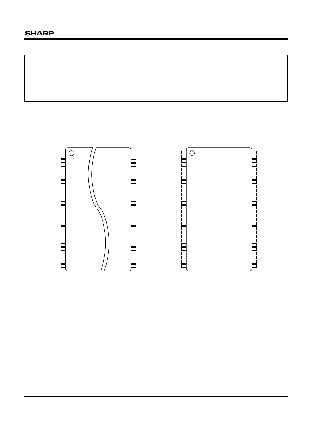
• Packages
– 56-pin TSOP Type I (TSOP056-P-1420)
Normal bend/Reverse bend
– 56-pin SSOP (SSOP056-P-0600)
★
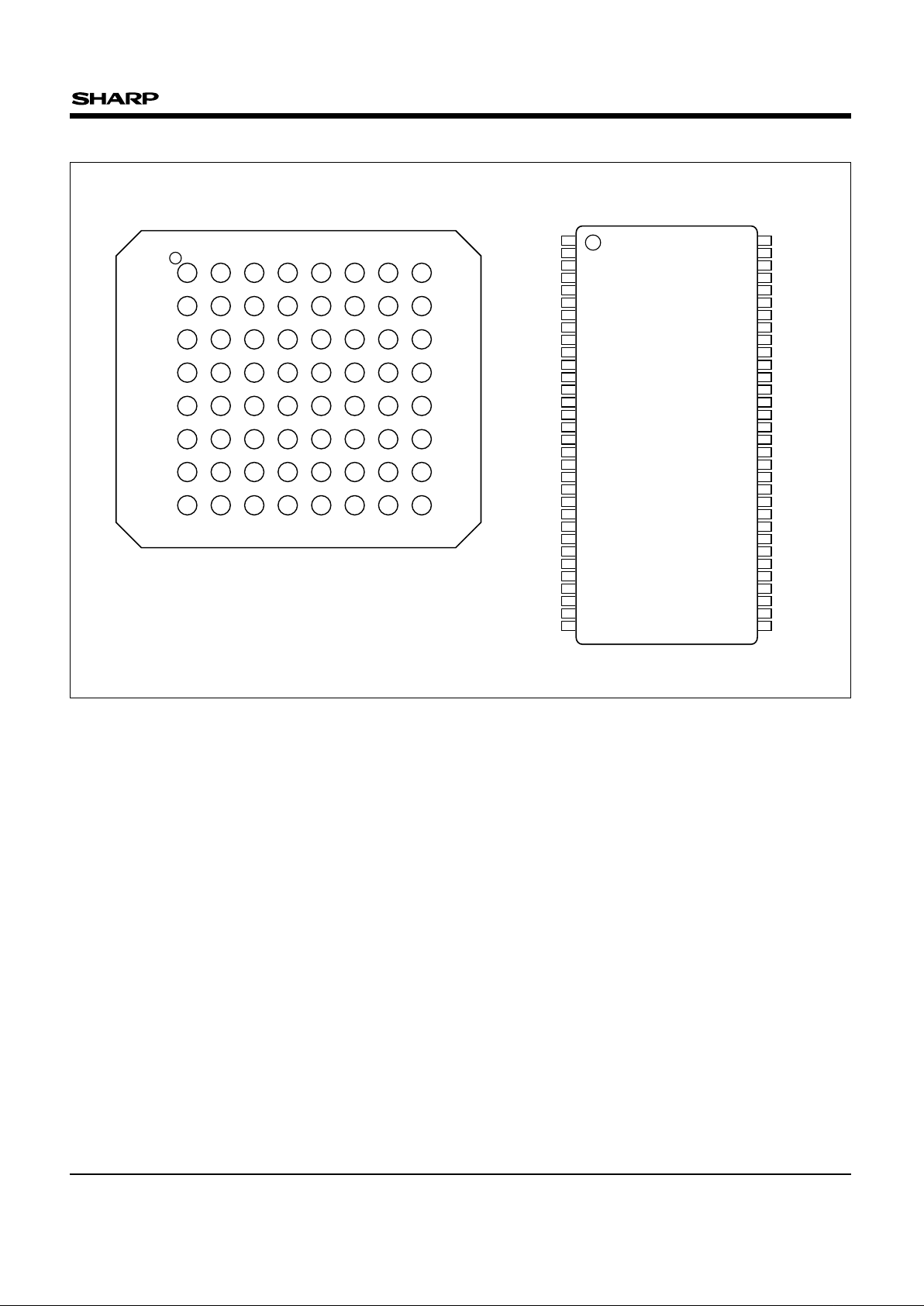
[LH28F160S5-L]
– 64-ball CSP (FBGA064-P-0811)
– 64-pin SDIP (SDIP064-P-0750)
★
∗ ETOX is a trademark of Intel Corporation.
★ Under development
LH28F160S5-L/S5H-L
16 M-bit (2 MB x 8/1 MB x 16) Smart 5
Flash Memories (Fast Programming)
- 1 -
In the absence of confirmation by device specification sheets, SHARP takes no responsibility for any defects that may occur in equipment using any SHARP devices shown in catalogs, data books,
etc. Contact SHARP in order to obtain the latest device specification sheets before using any SHARP device.
Page 2
LH28F160S5-L/S5H-L
- 2 -
PIN CONNECTIONS ★ Under development
56-PIN TSOP (Type I)
(TSOP056-P-1420)
NC
CE
1#
NC
A
20
A19
A18
A17
A16
VCC
A15
A14
A13
A12
CE0#
V
PP
RP#
A
11
A10
A9
A8
GND
A
7
A6
A5
A4
A3
A2
A1
1
2
3
4
5
6
7
8
9
10
11
12
13
14
15
16
17
18
19
20
21
22
23
24
25
26
27
28
56
55
54
53
52
51
50
49
48
47
46
45
44
43
42
41
40
39
38
37
36
35
34
33
32
31
30
29
WP#
WE#
OE#
STS
DQ
15
DQ7
DQ14
DQ6
GND
DQ
13
DQ5
DQ12
DQ4
VCC
GND
DQ
11
DQ3
DQ10
DQ2
VCC
DQ9
DQ1
DQ8
DQ0
A0
BYTE#
NC
NC
56-PIN SSOP★ [LH28F160S5-L]
(SSOP056-P-0600)
CE0#
A
12
A13
A14
A15
NC
CE
1#
NC
A
20
A19
A18
A17
A16
VCC
GND
DQ
6
DQ14
DQ7
DQ15
STS
OE#
WE#
WP#
DQ
13
DQ5
DQ12
DQ4
VCC
1
2
3
4
5
6
7
8
9
10
11
12
13
14
15
16
17
18
19
20
21
22
23
24
25
26
27
28
56
55
54
53
52
51
50
49
48
47
46
45
44
43
42
41
40
39
38
37
36
35
34
33
32
31
30
29
VPP
RP#
A
11
A10
A9
A1
A2
A3
A4
A5
A6
A7
GND
A
8
VCC
DQ9
DQ1
DQ8
DQ0
A0
BYTE#
NC
NC
DQ
2
DQ10
DQ3
DQ11
GND
TOP VIEW
NOTE :
Reverse bend available on request.
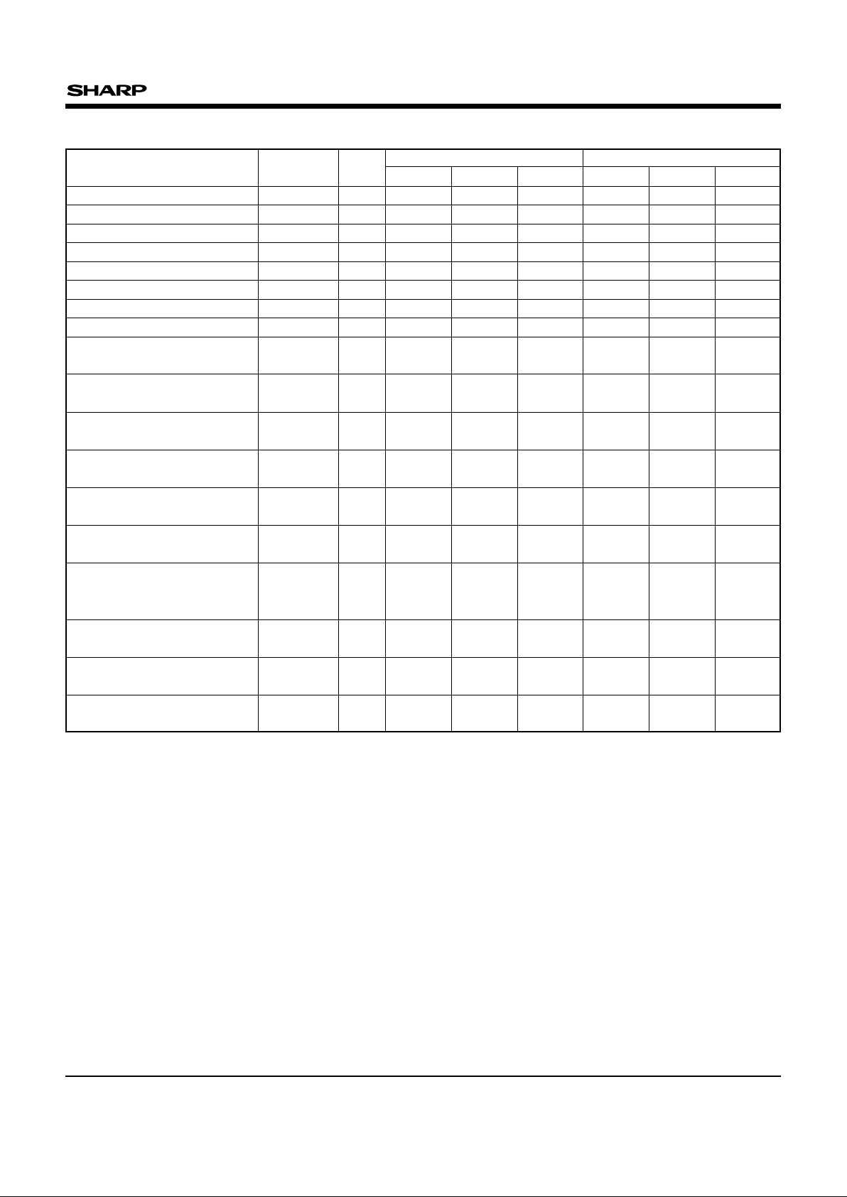
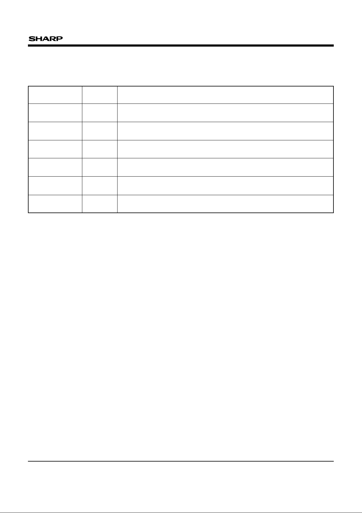
COMPARISON TABLE
VERSIONS
OPERATING
ACCESS TIME
DC CHARACTERISTICS
PACKAGE
TEMPERATURE
at 5.0±0.5 V
VCCdeep power-down current (MAX.)
LH28F160S5-L70/L10
0 to +70˚C 80 ns/100 ns 15 µA
56-pin TSOP (I), 56-pin SSOP
★
,
64-ball CSP, 64-pin SDIP
★
LH28F160S5H-L70/L10
–40 to +85˚C 90 ns/100 ns 20 µA
56-pin TSOP (I), 64-ball CSP,
64-pin SDIP
★
★ Under development
Page 3
LH28F160S5-L/S5H-L
- 3 -
TOP VIEW
PIN CONNECTIONS (contd.) ★ Under development
64-PIN SDIP
★
(SDIP064-P-0750)
VPP
RP#
A
11
A10
A9
A8
GND
A7
A6
A5
A4
A3
A2
A1
NC
NC
NC
NC
NC
NC
NC
BYTE#
A
0
DQ0
DQ8
DQ1
DQ9
VCC
DQ2
DQ10
DQ3
DQ11
1
2
3
4
5
6
7
8
9
10
11
12
13
14
15
16
17
18
19
20
21
22
23
24
25
26
27
28
29
30
31
32
64
63
62
61
60
59
58
57
56
55
54
53
52
51
50
49
48
47
46
45
44
43
42
41
40
39
38
37
36
35
34
33
CE0#
A
12
A13
A14
A15
VCC
A16
A17
A18
A19
A20
NC
CE
1#
NC
NC
NC
NC
WP#
WE#
OE#
STS
DQ
15
DQ7
DQ14
DQ6
GND
DQ
13
DQ5
DQ12
DQ4
VCC
GND
NC
1
A
A17
B
A15
C
A12
D
RP#
E
A
9
A20
2
A
18
VCC
CE0#
VPP
A8
NC NC
WP#
3
A14
A13
A11
A10
4
CE1#
NC
NC
GND
5
WE#
DQ6
NC
NC
DQ9
OE#
6
DQ15
DQ5
DQ12
DQ3
DQ10
STS
7
DQ7
GND
VCC
GND
VCC
NC
8
DQ14
DQ13
DQ4
DQ11
DQ2
F
A7G
NCA6A4A5A3A2A1
NCNCDQ0
BYTE#
DQ8A0DQ1
NC
H
A16
A19
(FBGA064-P-0811)
64-BALL CSP
Page 4
LH28F160S5-L/S5H-L
- 4 -
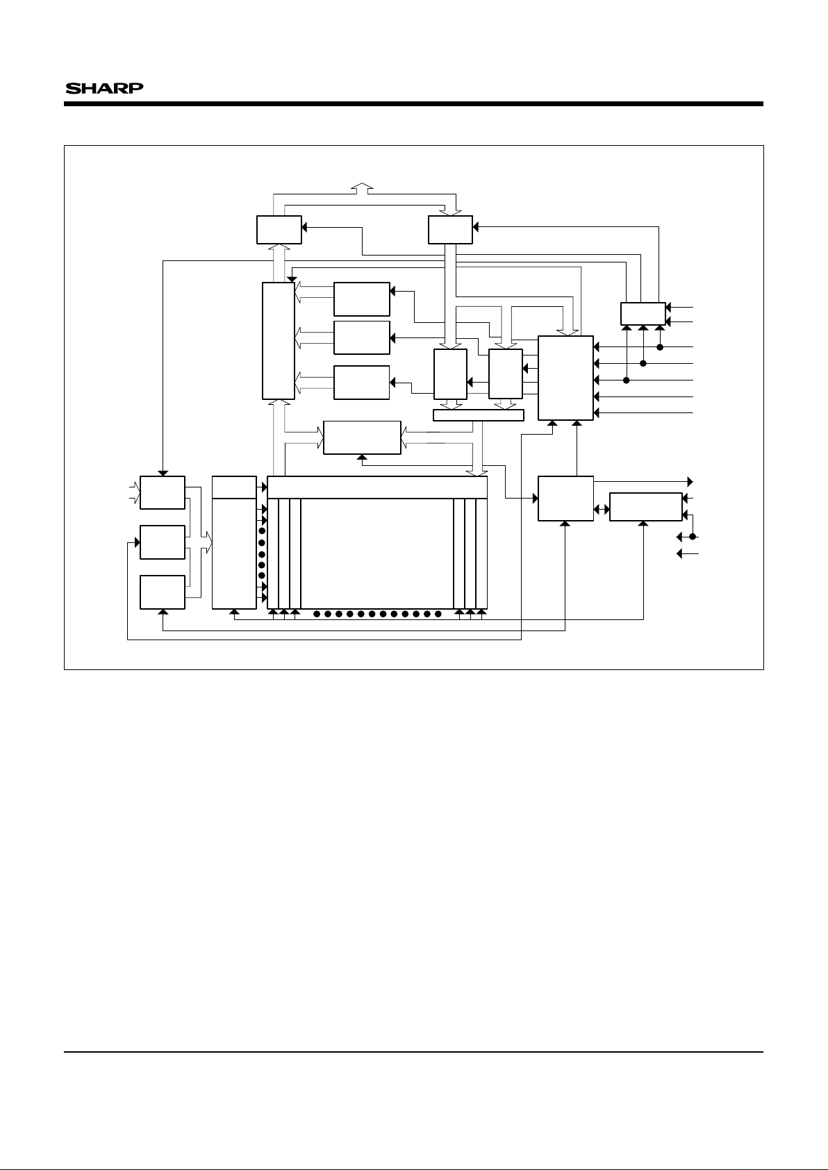
BLOCK DIAGRAM
OUTPUT
BUFFER
INPUT
BUFFER
I/O LOGIC
COMMAND
USER
INTERFACE
CE#
WE#
RP#
OE#
IDENTIFIER
REGISTER
STATUS
REGISTER
DATA
COMPARATOR
Y GATING
Y
DECODER
X
DECODER
32
64 k-BYTE
BLOCKS
INPUT
BUFFER
ADDRESS
LATCH
ADDRESS
COUNTER
WRITE STATE
MACHINE
PROGRAM/ERASE
VOLTAGE SWITCH
STS
GND
QUERY
ROM
DATA
REGISTER
WP#
BYTE#
MULTIPLEXER
PAGE
BUFFER
OUTPUT
MULTIPLEXER
VCC
VPP
VCC
A
0-A20
DQ0-DQ15
Page 5
LH28F160S5-L/S5H-L
- 5 -
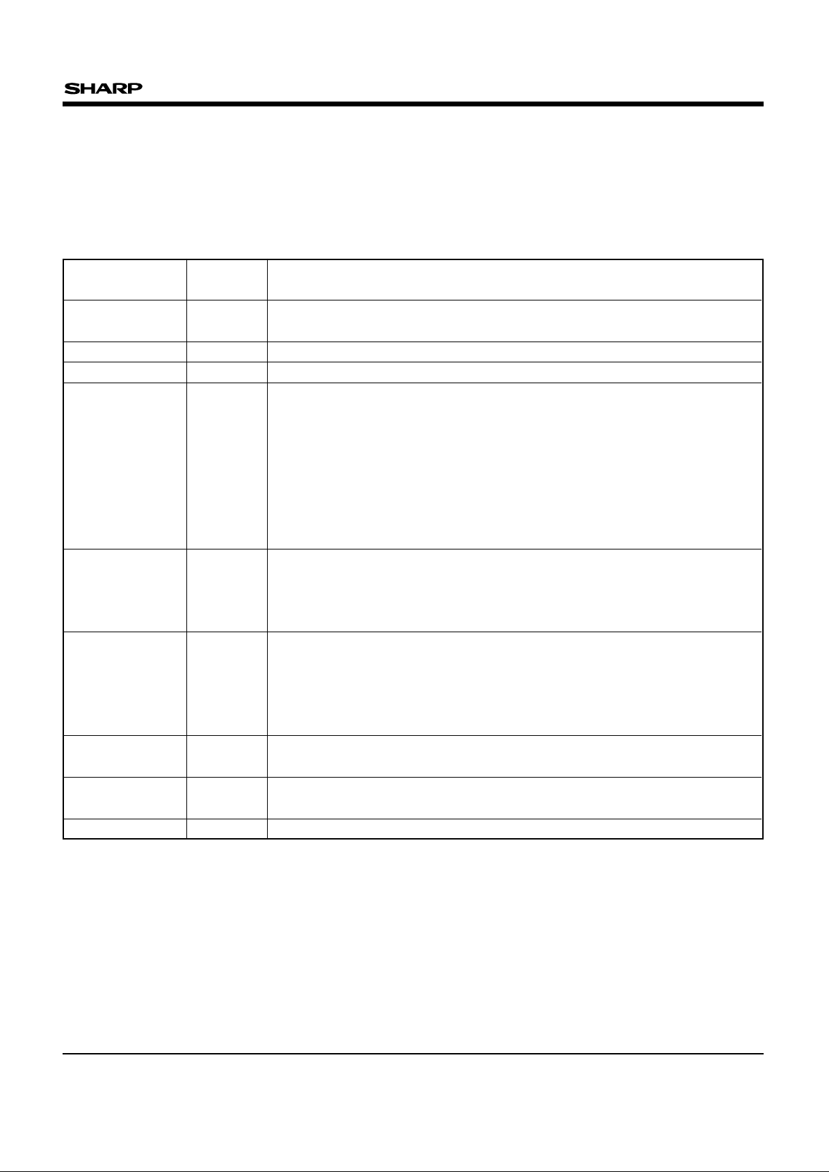
PIN DESCRIPTION
SYMBOL TYPE NAME AND FUNCTION
ADDRESS INPUTS : Inputs for addresses during read and write operations. Addresses
are internally latched during a write cycle.
A
0-A20 INPUT
A
0 : Byte Select Address. Not used in x16 mode (can be floated).
A
1-A4 : Column Address. Selects 1 of 16-bit lines.
A
5-A15 : Row Address. Selects 1 of 2 048-word lines.
A16-A20 : Block Address.
DATA INPUT/OUTPUTS :
DQ
0-DQ7 : Inputs data and commands during CUI write cycles; outputs data during
memory array, status register, query, and identifier code read cycles. Data pins float to
high-impedance when the chip is deselected or outputs are disabled. Data is internally
latched during a write cycle.
DQ
8-DQ15 : Inputs data during CUI write cycles in x16 mode; outputs data during memory
array read cycles in x16 mode; not used for statusregister, query and identifier code read
mode. Data pins float to high-impedance when the chip is deselected, outputs are
disabled, or in x8 mode (BYTE# = VIL). Data is internally latched during a write cycle.
CE
0#, CE1# INPUT
CHIP ENABLE : Activates the device’s control logic, input buffers decoders, and sense
amplifiers. Either CE
0# or CE1# VIH deselects the device and reduces power
consumption to standby levels. Both CE0# and CE1# must be VIL to select the devices.
RP# INPUT
RESET/DEEP POWER-DOWN : Puts the device in deep power-down mode and resets
internal automation. RP# V
IH enables normal operation. When driven VIL, RP# inhibits
write operations which provide data protection during power transitions. Exit from deep
power-down sets the device to read array mode.
OE# INPUT OUTPUT ENABLE : Gates the device’s outputs during a read cycle.
WE# INPUT
WRITE ENABLE : Controls writes to the CUI and array blocks. Addresses and data are
latched on the rising edge of the WE# pulse.
STS (RY/BY#) : Indicates the status of the internal WSM. When configured in level
mode (default mode), it acts as a RY/BY# pin. When low, the WSM is performing an
internal operation (block erase, full chip erase, (multi) word/byte write or block lock-bit
configuration). STS High Z indicates that the WSM is ready for new commands, block
erase is suspended, and (multi) word/byte write is inactive, (multi) word/byte write is
suspended or the device is in deep power-down mode. For alternate configurations of
the STATUS pin, see the Configuration command (Table 3 and Section 4.14).
WP# INPUT
WRITE PROTECT : Master control for block locking. When V
IL, locked blocks can not
be erased and programmed, and block lock-bits can not be set and reset.
BYTE# INPUT
BYTE ENABLE : BYTE# V
IL places device in x8 mode. All data are then input or output
on DQ
0-7, and DQ8-15 float. BYTE# VIH places the device in x16 mode, and turns off the
A0 input buffer.
BLOCK ERASE, FULL CHIP ERASE, (MULTI) WORD/BYTE WRITE, BLOCK LOCKBIT CONFIGURATION POWER SUPPLY : For erasing array blocks, writing bytes or
configuring block lock-bits. With V
PP
≤
V
PPLK, memory contents cannot be altered. Block
erase, full chip erase, (multi) word/byte write and block lock-bit configuration with an
invalid V
PP (see Section 6.2.3 "DC CHARACTERISTICS") produce spurious results
and should not be attempted.
V
CC SUPPLY
DEVICE POWER SUPPLY : Internal detection configures the device for 5 V operation.
Do not float any power pins. With V
CC
≤
V
LKO, all write attempts to the flash memory
are inhibited. Device operations at invalid V
CC voltage (see Section 6.2.3 "DC
CHARACTERISTICS") produce spurious results and should not be attempted.
GND SUPPLY GROUND : Do not float any ground pins.
NC NO CONNECT : Lead is not internal connected; recommend to be floated.
DQ0-DQ15
INPUT/
OUTPUT
OPEN
STS DRAIN
OUTPUT
V
PP SUPPLY
Page 6
1 INTRODUCTION
This datasheet contains LH28F160S5-L/S5H-L
specifications. Section 1 provides a flash memory
overview. Sections 2, 3, 4, and 5 describe the
memory organization and functionality. Section 6
covers electrical specifications. LH28F160S5-L/
S5H-L flash memories documentation also includes
ordering information which is referenced in
Section 7.
1.1 Product Overview
The LH28F160S5-L/S5H-L are high-performance
16 M-bit Smart 5 flash memories organized as
2 MB x 8/1 MB x 16. The 2 MB of data is arranged
in thirty-two 64 k-byte blocks which are individually
erasable, lockable, and unlockable in-system. The
memory map is shown in Fig.1.
Smart 5 technology provides a choice of V
CC and
V
PP combination, as shown in Table 1, to meet
system performance and power expectations. V
PP
at 5 V eliminates the need for a separate 12 V
converter, while V
PP = 5 V maximizes erase and
write performance. In addition to flexible erase and
program voltages, the dedicated V
PP pin gives
complete data protection when V
PP ≤ VPPLK.
Table 1 VCC and VPP Voltage Combination
Offered by Smart 5 Technology
Internal VCC and VPP detection circuitry automatically configures the device for optimized read
and write operations.
A Command User Interface (CUI) serves as the
interface between the system processor and
internal operation of the device. A valid command
sequence written to the CUI initiates device
automation. An internal Write State Machine (WSM)
automatically executes the algorithms and timings
necessary for block erase, full chip erase, (multi)
word/byte write and block lock-bit configuration
operations.
A block erase operation erases one of the device’s
64 k-byte blocks typically within 0.34 second (5 V
V
CC, 5 V VPP) independent of other blocks. Each
block can be independently erased 100 000 times
(3.2 million block erases per device). Block erase
suspend mode allows system software to suspend
block erase to read data from, or write data to any
other block.
A word/byte write is performed in byte increments
typically within 9.24 µs (5 V V
CC, 5 V VPP). A multi
word/byte write has high speed write performance
of 2 µs/byte (5 V V
CC, 5 V VPP). (Multi) word/byte
write suspend mode enables the system to read
data from, or write data to any other flash memory
array location.
Individual block locking uses a combination of bits
and WP#, thirty-two block lock-bits, to lock and
unlock blocks. Block lock-bits gate block erase, full
chip erase and (multi) word/byte write operations.
Block lock-bit configuration operations (Set Block
Lock-Bit and Clear Block Lock-Bits commands) set
and cleared block lock-bits.
The status register indicates when the WSM’s block
erase, full chip erase, (multi) word/byte write or
block lock-bit configuration operation is finished.
The STS output gives an additional indicator of
WSM activity by providing both a hardware signal
of status (versus software polling) and status
masking (interrupt masking for background block
erase, for example). Status polling using STS
minimizes both CPU overhead and system power
consumption. STS pin can be configured to
different states using the Configuration command.
The STS pin defaults to RY/BY# operation. When
low, STS indicates that the WSM is performing a
VCC VOLTAGE VPP VOLTAGE
5 V 5 V
LH28F160S5-L/S5H-L
- 6 -
Page 7
- 7 -
LH28F160S5-L/S5H-L
block erase, full chip erase, (multi) word/byte write
or block lock-bit configuration. STS High Z indicates
that the WSM is ready for a new command, block
erase is suspended and (multi) word/byte write are
inactive, (multi) word/byte write are suspended, or
the device is in deep power-down mode. The other
3 alternate configurations are all pulse mode for
use as a system interrupt.
The access time is 70 ns (t
AVQV) at the VCC supply
voltage range of 4.75 to 5.25 V over the temperature
range, 0 to +70°C (LH28F160S5-L)/
–40 to +85°C
(LH28F160S5H-L). At 4.5 to 5.5 V V
CC, the access
time is 80 ns/100 ns (LH28F160S5-L70/S5-L10) or
90 ns/100 ns (LH28F160S5H-L70/S5H-L10).
The Automatic Power Saving (APS) feature
substantially reduces active current when the
device is in static mode (addresses not switching).
In APS mode, the typical I
CCR current is 1 mA at
5 V V
CC.
When either CE
0# or CE1#, and RP# pins are at
V
CC, the ICC CMOS standby mode is enabled.
When the RP# pin is at GND, deep power-down
mode is enabled which minimizes power
consumption and provides write protection during
reset. A reset time (t
PHQV) is required from RP#
switching high until outputs are valid. Likewise, the
device has a wake time (t
PHEL) from RP#-high until
writes to the CUI are recognized. With RP# at
GND, the WSM is reset and the status register is
cleared.
Fig. 1 Memory Map
64 k-Byte Block
64 k-Byte Block
64 k-Byte Block
64 k-Byte Block
64 k-Byte Block
64 k-Byte Block
64 k-Byte Block
64 k-Byte Block
64 k-Byte Block
64 k-Byte Block
64 k-Byte Block
64 k-Byte Block
64 k-Byte Block
64 k-Byte Block
64 k-Byte Block
64 k-Byte Block
64 k-Byte Block
64 k-Byte Block
64 k-Byte Block
64 k-Byte Block
64 k-Byte Block
64 k-Byte Block
64 k-Byte Block
64 k-Byte Block
64 k-Byte Block
64 k-Byte Block
64 k-Byte Block
64 k-Byte Block
64 k-Byte Block
64 k-Byte Block
64 k-Byte Block
64 k-Byte Block
1FFFFF
1F0000
1EFFFF
1E0000
1DFFFF
1D0000
1CFFFF
1C0000
1BFFFF
1B0000
1AFFFF
1A0000
19FFFF
190000
18FFFF
180000
17FFFF
170000
16FFFF
160000
15FFFF
150000
14FFFF
140000
13FFFF
130000
12FFFF
120000
11FFFF
110000
10FFFF
100000
0FFFFF
0F0000
0EFFFF
0E0000
0DFFFF
0D0000
0CFFFF
0C0000
0BFFFF
0B0000
0AFFFF
0A0000
09FFFF
090000
08FFFF
080000
07FFFF
070000
06FFFF
060000
05FFFF
050000
04FFFF
040000
03FFFF
030000
02FFFF
020000
01FFFF
010000
00FFFF
000000
31
30
29
28
27
26
25
24
23
22
21
20
19
18
17
16
15
14
13
12
11
10
9
8
7
6
5
4
3
2
1
0
Page 8

2 PRINCIPLES OF OPERATION
The LH28F160S5-L/S5H-L flash memories include
an on-chip WSM to manage block erase, full chip
erase, (multi) word/byte write and block lock-bit
configuration functions. It allows for : 100% TTLlevel control inputs, fixed power supplies during
block erase, full chip erase, (multi) word/byte write
and block lock-bit configuration, and minimal
processor overhead with RAM-like interface timings.
After initial device power-up or return from deep
power-down mode (see Table 2.1 and Table 2.2
"Bus Operations"), the device defaults to read
array mode. Manipulation of external memory
control pins allow array read, standby, and output
disable operations.
Status register, query structure and identifier codes
can be accessed through the CUI independent of
the V
PP voltage. High voltage on VPP enables
successful block erase, full chip erase, (multi)
word/byte write and block lock-bit configuration. All
functions associated with altering memory
contents—block erase, full chip erase, (multi)
word/byte write and block lock-bit configuration,
status, query and identifier codes—are accessed
via the CUI and verified through the status register.
Commands are written using standard microprocessor write timings. The CUI contents serve as
input to the WSM, which controls the block erase,
full chip erase, (multi) word/byte write and block
lock-bit configuration. The internal algorithms are
regulated by the WSM, including pulse repetition,
internal verification, and margining of data.
Addresses and data are internally latched during
write cycles. Writing the appropriate command
outputs array data, accesses the identifier codes,
outputs query structure or outputs status register
data.
Interface software that initiates and polls progress
of block erase, full chip erase, (multi) word/byte
write and block lock-bit configuration can be stored
in any block. This code is copied to and executed
from system RAM during flash memory updates.
After successful completion, reads are again
possible via the Read Array command. Block erase
suspend allows system software to suspend a
block erase to read/write data from/to blocks other
than that which is suspended. Write suspend allows
system software to suspend a (multi) word/byte
write to read data from any other flash memory
array location.
2.1 Data Protection
Depending on the application, the system designer
may choose to make the V
PP power supply
switchable (available only when block erase, full
chip erase, (multi) word/byte write and block lock-bit
configuration are required) or hardwired to V
PPH1.
The device accommodates either design practice
and encourages optimization of the processormemory interface.
When V
PP ≤ VPPLK, memory contents cannot be
altered. The CUI, with multi-step block erase, full
chip erase, (multi) word/byte write and block lock-bit
configuration command sequences, provides
protection from unwanted operations even when
high voltage is applied to V
PP. All write functions
are disabled when V
CC is below the write lockout
voltage V
LKO or when RP# is at VIL. The device’s
block locking capability provides additional
protection from inadvertent code or data alteration
by gating block erase, full chip erase and (multi)
word/byte write operations.
LH28F160S5-L/S5H-L
- 8 -
Page 9

3 BUS OPERATION
The local CPU reads and writes flash memory insystem. All bus cycles to or from the flash memory
conform to standard microprocessor bus cycles.
3.1 Read
Information can be read from any block, identifier
codes, query structure, or status register
independent of the V
PP voltage. RP# must be at
V
IH.
The first task is to write the appropriate read mode
command (Read Array, Read Identifier Codes,
Query or Read Status Register) to the CUI. Upon
initial device power-up or after exit from deep
power-down mode, the device automatically resets
to read array mode. Five control pins dictate the
data flow in and out of the component : CE#
(CE
0#, CE1#), OE#, WE#, RP# and WP#. CE0#,
CE
1# and OE# must be driven active to obtain data
at the outputs. CE
0# and CE1# are the device
selection control, and when active enables the
selected memory device. OE# is the data output
(DQ
0-DQ15) control and when active drives the
selected memory data onto the I/O bus. WE# and
RP# must be at V
IH. Fig. 15 and Fig. 16, illustrate
a read cycle.
3.2 Output Disable
With OE# at a logic-high level (VIH), the device
outputs are disabled. Output pins DQ
0-DQ15 are
placed in a high-impedance state.
3.3 Standby
Either CE0# or CE1# at a logic-high level (VIH)
places the device in standby mode which
substantially reduces device power consumption.
DQ
0-DQ15 outputs are placed in a high-impedance
state independent of OE#. If deselected during
block erase, full chip erase, (multi) word/byte write
and block lock-bit configuration, the device
continues functioning, and consuming active power
until the operation completes.
3.4 Deep Power-Down
RP# at VIL initiates the deep power-down mode.
In read modes, RP#-low deselects the memory,
places output drivers in a high-impedance state and
turns off all internal circuits. RP# must be held low
for a minimum of 100 ns. Time t
PHQV is required
after return from power-down until initial memory
access outputs are valid. After this wake-up
interval, normal operation is restored. The CUI is
reset to read array mode and status register is set
to 80H.
During block erase, full chip erase, (multi) word/byte
write or block lock-bit configuration modes, RP#-low
will abort the operation. STS remains low until the
reset operation is complete. Memory contents being
altered are no longer valid; the data may be
partially erased or written. Time t
PHWL is required
after RP# goes to logic-high (V
IH) before another
command can be written.
As with any automated device, it is important to
assert RP# during system reset. When the system
comes out of reset, it expects to read from the flash
memory. Automated flash memories provide status
information when accessed during block erase, full
chip erase, (multi) word/byte write and block lock-bit
configuration. If a CPU reset occurs with no flash
memory reset, proper CPU initialization may not
occur because the flash memory may be providing
status information instead of array data. SHARP’s
flash memories allow proper CPU initialization
following a system reset through the use of the
RP# input. In this application, RP# is controlled by
the same RESET# signal that resets the system
CPU.
LH28F160S5-L/S5H-L
- 9 -
Page 10
- 10 -
LH28F160S5-L/S5H-L
3.5 Read Identifier Codes Operation
The read identifier codes operation outputs the
manufacture code, device code, block status codes
for each block (see Fig. 2). Using the manufacture
and device codes, the system CPU can
automatically match the device with its proper
algorithms. The block status codes identify locked
or unlocked block setting and erase completed or
erase uncompleted condition.
Fig. 2 Device Identifier Code Memory Map
3.6 Query Operation
The query operation outputs the query structure.
Query database is stored in the 48-byte ROM.
Query structure allows system software to gain
critical information for controlling the flash
component. Query structures are always presented
on the lowest-order data output (DQ
0-DQ7) only.
3.7 Write
Writing commands to the CUI enable reading of
device data and identifier codes. They also control
inspection and clearing of the status register. When
V
CC = VCC1/2 and V PP = VPPH1, the CUI additionally
controls block erase, full chip erase, (multi)
word/byte write and block lock-bit configuration.
The Block Erase command requires appropriate
command data and an address within the block to
be erased. The Word/Byte Write command requires
the command and address of the location to be
written. Set Block Lock-Bit command requires the
command and block address within the device
(Block Lock) to be locked. The Clear Block LockBits command requires the command and address
within the device.
The CUI does not occupy an addressable memory
location. It is written when WE# and CE# are
active. The address and data needed to execute a
command are latched on the rising edge of WE# or
CE# (whichever goes high first). Standard
microprocessor write timings are used. Fig. 17 and
Fig. 18 illustrate WE# and CE#-controlled write
operations.
4 COMMAND DEFINITIONS
When the VPP voltage ≤ VPPLK, read operations
from the status register, identifier codes, query, or
blocks are enabled. Placing V
PPH1 on VPP enables
successful block erase, full chip erase, (multi)
word/byte write and block lock-bit configuration
operations.
Device operations are selected by writing specific
commands into the CUI. Table 3 defines these
commands.
1FFFFF
1F0006
1F0005
1F0004
1F0003
1F0000
1EFFFF
020000
01FFFF
010006
010005
010004
010003
010000
00FFFF
000006
000005
000004
000003
000002
000001
000000
Reserved for
Future Implementation
Block 31 Status Code
Block 31
Block 1
Block 0
(Blocks 2 through 30)
Reserved for
Future Implementation
Reserved for
Future Implementation
Block 1 Status Code
Reserved for
Future Implementation
Reserved for
Future Implementation
Block 0 Status Code
Device Code
Manufacture Code
Page 11
- 11 -
LH28F160S5-L/S5H-L
Table 2.1 Bus Operations (BYTE# = VIH)
MODE NOTE RP# CE0#CE1# OE# WE#
ADDRESS
VPP DQ0-15 STS
Read
1, 2, 3, 9
VIH VIL VIL VIL VIH XXDOUT X
Output Disable 3 VIH VIL VIL VIH VIH X X High Z X
V
IH VIH
Standby 3 VIH VIH VIL X X X X High Z X
VIL VIH
Deep Power-Down 4 VIL X X X X X X High Z High Z
Read Identifier
9V
IH VIL VIL VIL VIH
See
X(
NOTE 5)
High Z
Codes
Fig. 2
Query 9 V
IH VIL VIL VIL VIH
See Table
X(
NOTE 6)
High Z
6 through 10
Write
3, 7, 8, 9
VIH VIL VIL VIH VIL XXDIN X
Table 2.2 Bus Operations (BYTE# = VIL)
MODE NOTE RP# CE0#CE1# OE# WE#
ADDRESS
VPP DQ0-7 STS
Read
1, 2, 3, 9
VIH VIL VIL VIL VIH XXDOUT X
Output Disable 3 VIH VIL VIL VIH VIH X X High Z X
VIH VIH
Standby 3 VIH VIH VIL X X X X High Z X
VIL VIH
Deep Power-Down 4 VIL X X X X X X High Z High Z
Read Identifier
9V
IH VIL VIL VIL VIH
See
X
(NOTE 5)
High Z
Codes
Fig. 2
Query 9 V
IH VIL VIL VIL VIH
See Table
X
(NOTE 6)
High Z
6 through 10
Write
3, 7, 8, 9
VIH VIL VIL VIH VIL XXDIN X
NOTES :
1. Refer to Section 6.2.3 "DC CHARACTERISTICS".
When V
PP ≤ VPPLK, memory contents can be read, but
not altered.
2. X can be V
IL or VIH for control pins and addresses, and
V
PPLK or VPPH1 for VPP. See Section 6.2.3 "DC
CHARACTERISTICS
" for VPPLK and VPPH1 voltages.
3. STS is V
OL (if configured to RY/BY# mode) when the
WSM is executing internal block erase, full chip erase,
(multi) word/byte write or block lock-bit configuration
algorithms. It is floated during when the WSM is not
busy, in block erase suspend mode with (multi)
word/byte write inactive, (multi) word/byte write suspend
mode, or deep power-down mode.
4. RP# at GND±0.2 V ensures the lowest deep powerdown current.
5. See Section 4.2 for read identifier code data.
6. See Section 4.5 for query data.
7. Command writes involving block erase, full chip erase,
(multi) word/byte write or block lock-bit configuration are
reliably executed when V
PP = VPPH1 and VCC = VCC1/2.
8. Refer to Table 3 for valid D
IN during a write operation.
9. Don’t use the timing both OE# and WE# are V
IL.
Page 12
LH28F160S5-L/S5H-L
- 12 -
Table 3 Command Definitions
(NOTE 10)
COMMAND
BUS CYCLES
NOTE
FIRST BUS CYCLE SECOND BUS CYCLE
REQ’D.
Oper
(NOTE 1)
Addr
(NOTE 2)
Data
(NOTE 3)
Oper
(NOTE 1)
Addr
(NOTE 2)
Data
(NOTE 3)
Read Array/Reset 1 Write X FFH
Read Identifier Codes ≥ 2 4 Write X 90H Read IA ID
Query ≥ 2 Write X 98H Read QA QD
Read Status Register 2 Write X 70H Read X SRD
Clear Status Register 1 Write X 50H
Block Erase Setup/Confirm 2 5 Write BA 20H Write BA D0H
Full Chip Erase Setup/Confirm
2 Write X 30H Write X D0H
Word/Byte Write Setup/Write 2 5, 6 Write WA 40H Write WA WD
Alternate Word/Byte Write
2 5, 6 Write WA 10H Write WA WD
Setup/Write
Multi Word/Byte Write
≥ 4 9 Write WA E8H Write WA N
–1
Setup/Confirm
Block Erase and (Multi)
1 5 Write X B0H
Word/Byte Write Suspend
Confirm and Block Erase and
1 5 Write X D0H
(Multi) Word/Byte Write Resume
Block Lock-Bit Set
2 7 Write BA 60H Write BA 01H
Setup/Confirm
Block Lock-Bit Reset
2 8 Write X 60H Write X D0H
Setup/Confirm
STS Configuration
Level-Mode for Erase 2 Write X B8H Write X 00H
and Write (RY/BY# Mode)
STS Configuration
2 Write X B8H Write X 01H
Pulse-Mode for Erase
STS Configuration
2 Write X B8H Write X 02H
Pulse-Mode for Write
STS Configuration Pulse-Mode
2 Write X B8H Write X 03H
for Erase and Write
NOTES :
1. Bus operations are defined in Table 2.1 and Table 2.2.
2. X = Any valid address within the device.
IA = Identifier code address : see Fig. 2.
QA = Query offset address.
BA = Address within the block being erased or locked.
WA = Address of memory location to be written.
3. SRD = Data read from status register. See Table 13.1
for a description of the status register bits.
WD = Data to be written at location WA. Data is latched
on the rising edge of WE# or CE# (whichever
goes high first).
ID = Data read from identifier codes.
QD = Data read from query database.
4. Following the Read Identifier Codes command, read
operations access manufacture, device and block status
codes. See Section 4.2 for read identifier code data.
5. If the block is locked, WP# must be at V
IH to enable
block erase or (multi) word/byte write operations.
Attempts to issue a block erase or (multi) word/byte write
to a locked block while RP# is V
IH.
6. Either 40H or 10H is recognized by the WSM as the
byte write setup.
7. A block lock-bit can be set while WP# is V
IH.
8. WP# must be at V
IH to clear block lock-bits. The clear
block lock-bits operation simultaneously clears all block
lock-bits.
9. Following the Third Bus Cycle, inputs the write address
and write data of "N" times. Finally, input the confirm
command "D0H".
10. Commands other than those shown above are reserved
by SHARP for future device implementations and should
not be used.
Page 13
- 13 -
LH28F160S5-L/S5H-L
4.1 Read Array Command
Upon initial device power-up and after exit from
deep power-down mode, the device defaults to
read array mode. This operation is also initiated by
writing the Read Array command. The device
remains enabled for reads until another command
is written. Once the internal WSM has started a
block erase, full chip erase, (multi) word/byte write
or block lock-bit configuration, the device will not
recognize the Read Array command until the WSM
completes its operation unless the WSM is
suspended via an Erase Suspend and (Multi)
Word/Byte Write Suspend command. The Read
Array command functions independently of the V
PP
voltage and RP# must be VIH.
4.2 Read Identifier Codes Command
The identifier code operation is initiated by writing
the Read Identifier Codes command. Following the
command write, read cycles from addresses shown
in Fig. 2 retrieve the manufacture, device, block
lock configuration and block erase status (see
Table 4 for identifier code values). To terminate the
operation, write another valid command. Like the
Read Array command, the Read Identifier Codes
command functions independently of the V
PP
voltage and RP# must be VIH. Following the Read
Identifier Codes command, the following information
can be read :
Table 4 Identifier Codes
NOTE :
1. X selects the specific block status code to be read. See
Fig. 2 for the device identifier code memory map.
4.3 Read Status Register Command
The status register may be read to determine when
a block erase, full chip erase, (multi) word/byte
write or block lock-bit configuration is complete and
whether the operation completed successfully (see
Table 13.1). It may be read at any time by writing
the Read Status Register command. After writing
this command, all subsequent read operations
output data from the status register until another
valid command is written. The status register
contents are latched on the falling edge of OE# or
CE# (Either CE
0# or CE1#), whichever occurs. OE#
or CE# (Either CE
0# or CE1#) must toggle to VIH
before further reads to update the status register
latch. The Read Status Register command
functions independently of the V
PP voltage. RP#
must be V
IH.
The extended status register may be read to
determine multi byte write availability (see Table
13.2). The extended status register may be read at
any time by writing the Multi Byte Write command.
After writing this command, all subsequent read
operations output data from the extended status
register, until another valid command is written. The
contents of the extended status register are latched
on the falling edge of OE# or CE# (Either CE
0# or
CE
1#), whichever occurs last in the read cycle.
Multi Byte Write command must be re-issued to
update the extended status register latch.
4.4 Clear Status Register Command
Status register bits SR.5, SR.4, SR.3 and SR.1 are
set to "1"s by the WSM and can only be reset by
the Clear Status Register command. These bits
indicate various failure conditions (see Table 13.1).
By allowing system software to reset these bits,
several operations (such as cumulatively erasing or
locking multiple blocks or writing several bytes in
CODE ADDRESS DATA
Manufacture Code
00000H
B0
00001H
Device Code
00002H
D0
00003H
Block Status Code
X0004H
(NOTE 1)
X0005H
(NOTE 1)
•
Block is Unlocked DQ
0 = 0
•
Block is Locked DQ
0 = 1
•
Last erase operation
completed successfully
DQ
1 = 0
•
Last erase operation did
DQ
1 = 1
not completed successfully
•Reserved for Future Use DQ
2-7
Page 14
LH28F160S5-L/S5H-L
- 14 -
sequence) may be performed. The status register
may be polled to determine if an error occurs
during the sequence.
To clear the status register, the Clear Status
Register command (50H) is written. It functions
independently of the applied V
PP voltage. RP#
must be V
IH. This command is not functional during
block erase, full chip erase, (multi) word/byte write,
block lock-bit configuration, block erase suspend or
(multi) word/byte write suspend modes.
4.5 Query Command
Query database can be read by writing Query
command (98H). Following the command write,
read cycle from address shown in Table 6 through
Table 10 retrieve the critical information to write,
erase and otherwise control the flash component.
A
0 of query offset address is ignored when x8
mode (BYTE# = V
IL).
Query data are always presented on the low-byte
data output (DQ
0-DQ7). In x16 mode, high-byte
(DQ
8-DQ15) outputs 00H. The bytes not assigned
to any information or reserved for future use are set
to "0". This command functions independently of
the V
PP voltage. RP# must be VIH.
Table 5 Example of Query Structure Output
4.5.1 BLOCK STATUS REGISTER
This field provides lock configuration and erase
status for the specified block. These informations
are only available when device is ready (SR.7 = 1).
If block erase or full chip erase operation is finished
irregularly, block erase status bit will be set to "1". If
bit 1 is "1", this block is invalid.
MODE OFFSET ADDRESS
OUTPUT
DQ15-8 DQ7-0
A5, A4, A3, A2, A1, A0
1, 0, 0, 0, 0, 0 (20H) High Z "Q"
x8 mode 1, 0, 0, 0, 0, 1 (21H) High Z "Q"
1, 0, 0, 0, 1, 0 (22H) High Z "R"
1, 0, 0, 0, 1, 1 (23H) High Z "R"
A5, A4, A3, A2, A1
x16 mode
1, 0, 0, 0, 0 (10H) 00H "Q"
1, 0, 0, 0, 1 (11H) 00H "R"
Table 6 Query Block Status Register
OFFSET
LENGTH DESCRIPTION
(Word Address)
(BA+2)H 01H Block Status Register
bit0 Block Lock Configuration
0 = Block is unlocked
1 = Block is locked
bit1 Block Erase Status
0 = Last erase operation completed successfully
1 = Last erase operation not completed successfully
bit2-7 Reserved for future use
NOTE :
BA = The beginning of a Block Address.
Page 15
LH28F160S5-L/S5H-L
- 15 -
4.5.2 CFI QUERY IDENTIFICATION STRING
The identification string provides verification that the
component supports the Common Flash Interface
specification. Additionally, it indicates which version
of the spec and which vendor-specified command
set(s) is(are) supported.
Table 7 CFI Query Identification String
OFFSET
LENGTH DESCRIPTION
(Word Address)
10H, 11H, 12H 03H Query Unique ASCII string "QRY"
51H, 52H, 59H
13H, 14H 02H Primary Vendor Command Set and Control Interface ID Code
01H, 00H (SCS ID Code)
15H, 16H 02H Address for Primary Algorithm Extended Query Table
31H, 00H (SCS Extended Query Table Offset)
17H, 18H 02H Alternate Vendor Command Set and Control Interface ID Code
0000H (0000H means that no alternate exists)
19H, 1AH 02H Address for Alternate Algorithm Extended Query Table
0000H (0000H means that no alternate exists)
4.5.3 SYSTEM INTERFACE INFORMATION
The following device information can be useful in optimizing system interface software.
Table 8 System Information String
OFFSET
LENGTH DESCRIPTION
(Word Address)
1BH 01H V
CC Logic Supply Minimum Write/Erase voltage
27H (2.7 V)
1CH 01H V
CC Logic Supply Maximum Write/Erase voltage
55H (5.5 V)
1DH 01H V
PP Programming Supply Minimum Write/Erase voltage
27H (2.7 V)
1EH 01H V
PP Programming Supply Maximum Write/Erase voltage
55H (5.5 V)
1FH 01H Typical Time-Out per Single Byte/Word Write
03H (23= 8 µs)
20H 01H Typical Time-Out for Maximum Size Buffer Write (32 Bytes)
06H (26= 64 µs)
21H 01H Typical Time-Out per Individual Block Erase
0AH (0AH = 10, 210= 1 024 ms)
22H 01H Typical Time-Out for Full Chip Erase
0FH (0FH = 15, 215= 32 768 ms)
23H 01H Maximum Time-Out per Single Byte/Word Write, 2
N
times of typical.
04H (24= 16, 8 µs x 16 = 128 µs)
24H 01H Maximum Time-Out per Maximum Size Buffer Write, 2
N
times of typical.
04H (24= 16, 64 µs x 16 = 1 024 µs)
25H 01H Maximum Time-Out per Individual Block Erase, 2
N
times of typical.
04H (24= 16, 1 024 ms x 16 = 16 384 ms)
26H 01H Maximum Time-Out for Full Chip Erase, 2
N
times of typical.
04H (2
4
= 16, 32 768 ms x 16 = 524 288 ms)
Page 16
LH28F160S5-L/S5H-L
4.5.4 DEVICE GEOMETRY DEFINITION
This field provides critical details of the flash device geometry.
Table 9 Device Geometry Definition
OFFSET
LENGTH DESCRIPTION
(Word Address)
27H 01H Device Size
15H (15H = 21, 221= 2 097 152 = 2 M Bytes)
28H, 29H 02H Flash Device Interface Description
02H, 00H (x8/x16 supports x8 and x16 via BYTE#)
2AH, 2BH 02H Maximum Number of Bytes in Multi Word/Byte Write
05H, 00H (25= 32 Bytes )
2CH 01H Number of Erase Block Regions within Device
01H (symmetrically blocked)
2DH, 2EH 02H The Number of Erase Blocks
1FH, 00H (1FH = 31 ⇒ 31 + 1 = 32 Blocks)
2FH, 30H 02H The Number of "256 Bytes" cluster in a Erase Block
00H, 01H (0100H = 256 ⇒ 256 Bytes x 256 = 64k Bytes in a Erase Block)
- 16 -
Page 17
LH28F160S5-L/S5H-L
4.5.5 SCS OEM SPECIFIC EXTENDED QUERY
TABLE
Certain flash features and commands may be
optional in a vendor-specific algorithm specification.
The optional vendor-specific query table(s) may be
used to specify this and other types of information.
These structures are defined solely by the flash
vendor(s).
Table 10 SCS OEM Specific Extended Query Table
OFFSET
LENGTH DESCRIPTION
(Word Address)
31H, 32H, 33H 03H PRI
50H, 52H, 49H
34H 01H 31H (1) Major Version Number , ASCII
35H 01H 30H (0) Minor Version Number, ASCII
36H, 37H, 04H 0FH, 00H, 00H, 00H
38H, 39H Optional Command Support
bit0 = 1 : Chip Erase Supported
bit1 = 1 : Suspend Erase Supported
bit2 = 1 : Suspend Write Supported
bit3 = 1 : Lock/Unlock Supported
bit4 = 0 : Queued Erase Not Supported
bit5-31 = 0 : Reserved for future use
3AH 01H 01H
Supported Functions after Suspend
bit0 = 1 : Write Supported after Erase Suspend
bit1-7 = 0 : Reserved for future use
3BH, 3CH 02H 03H, 00H
Block Status Register Mask
bit0 = 1 : Block Status Register Lock Bit [BSR.0] active
bit1 = 1 : Block Status Register Valid Bit [BSR.1] active
bit2-15 = 0 : Reserved for future use
3DH 01H VCC Logic Supply Optimum Write/Erase voltage (highest performance)
50H (5.0 V)
3EH 01H
VPPProgramming Supply Optimum Write/Erase voltage (highest performance)
50H (5.0 V)
3FH reserved Reserved for future versions of the SCS specification
- 17 -
Page 18

- 18 -
4.6 Block Erase Command
Block erase is executed one block at a time and
initiated by a two-cycle command. A block erase
setup is first written, followed by a block erase
confirm. This command sequence requires
appropriate sequencing and an address within the
block to be erased (erase changes all block data to
FFH). Block preconditioning, erase and verify are
handled internally by the WSM (invisible to the
system). After the two-cycle block erase sequence
is written, the device automatically outputs status
register data when read (see Fig. 3). The CPU can
detect block erase completion by analyzing the
output data of the STS pin or status register bit
SR.7.
When the block erase is complete, status register
bit SR.5 should be checked. If a block erase error
is detected, the status register should be cleared
before system software attempts corrective actions.
The CUI remains in read status register mode until
a new command is issued.
This two-step command sequence of set-up
followed by execution ensures that block contents
are not accidentally erased. An invalid Block Erase
command sequence will result in both status
register bits SR.4 and SR.5 being set to "1". Also,
reliable block erasure can only occur when V
CC =
VCC1/2 and VPP = VPPH1. In the absence of this
high voltage, block contents are protected against
erasure. If block erase is attempted while V
PP ≤
V
PPLK, SR.3 and SR.5 will be set to "1". Successful
block erase requires that the corresponding block
lock-bit be cleared or if set, that WP# = V
IH. If block
erase is attempted when the corresponding block
lock-bit is set and WP# = V
IL, SR.1 and SR.5 will
be set to "1".
4.7 Full Chip Erase Command
This command followed by a confirm command
(D0H) erases all of the unlocked blocks. A full chip
erase setup is first written, followed by a full chip
erase confirm. After a confirm command is written,
device erases the all unlocked blocks from block 0
to block 31 block by block. This command
sequence requires appropriate sequencing. Block
preconditioning, erase and verify are handled
internally by the WSM (invisible to the system).
After the two-cycle full chip erase sequence is
written, the device automatically outputs status
register data when read (see Fig. 4). The CPU can
detect full chip erase completion by analyzing the
output data of the STS pin or status register bit
SR.7.
When the full chip erase is complete, status register
bit SR.5 should be checked. If erase error is
detected, the status register should be cleared
before system software attempts corrective actions.
The CUI remains in read status register mode until
a new command is issued. If error is detected on a
block during full chip erase operation, WSM stops
erasing. Reading the block valid status by issuing
Read ID Codes command or Query command
informs which blocks failed to its erase.
This two-step command sequence of set-up
followed by execution ensures that block contents
are not accidentally erased. An invalid Full Chip
Erase command sequence will result in both status
register bits SR.4 and SR.5 being set to "1". Also,
reliable full chip erasure can only occur when V
CC =
VCC1/2 and VPP = VPPH1. In the absence of this high
voltage, block contents are protected against
erasure. If full chip erase is attempted while V
PP ≤
V
PPLK, SR.3 and SR.5 will be set to "1". When
WP# = V
IH, all blocks are erased independent of
block lock-bits status. When WP# = V
IL, only
unlocked blocks are erased. In this case, SR.1 and
SR.4 will not be set to "1". Full chip erase can not
be suspended.
LH28F160S5-L/S5H-L
Page 19

- 19 -
4.8 Word/Byte Write Command
Word/byte write is executed by a two-cycle
command sequence. Word/Byte Write setup
(standard 40H or alternate 10H) is written, followed
by a second write that specifies the address and
data (latched on the rising edge of WE#). The
WSM then takes over, controlling the word/byte
write and write verify algorithms internally. After the
word/byte write sequence is written, the device
automatically outputs status register data when
read (see Fig. 5). The CPU can detect the
completion of the word/byte write event by
analyzing the STS pin or status register bit SR.7.
When word/byte write is complete, status register
bit SR.4 should be checked. If word/byte write error
is detected, the status register should be cleared.
The internal WSM verify only detects errors for "1"s
that do not successfully write to "0"s. The CUI
remains in read status register mode until it
receives another command.
Reliable word/byte writes can only occur when V
CC
=
VCC1/2 and VPP = VPPH1. In the absence of this
high voltage, memory contents are protected
against word/byte writes. If word/byte write is
attempted while V
PP ≤ VPPLK, status register bits
SR.3 and SR.4 will be set to "1". Successful
word/byte write requires that the corresponding
block lock-bit be cleared or, if set, that WP# = V
IH.
If word/byte write is attempted when the
corresponding block lock-bit is set and WP# = V
IL,
SR.1 and SR.4 will be set to "1". Word/byte write
operations with V
IL < WP# < VIH produce spurious
results and should not be attempted.
4.9 Multi Word/Byte Write Command
Multi word/byte write is executed by at least fourcycle or up to 35-cycle command sequence. Up to
32 bytes in x8 mode (16 words in x16 mode) can
be loaded into the buffer and written to the flash
array. First, multi word/byte write setup (E8H) is
written with the write address. At this point, the
device automatically outputs extended status
register data (XSR) when read (see Fig. 6 and
Fig. 7). If extended status register bit XSR.7 is 0,
no Multi Word/Byte Write command is available and
multi word/byte write setup which just has been
written is ignored. To retry, continue monitoring
XSR.7 by writing multi word/byte write setup with
write address until XSR.7 transitions to "1". When
XSR.7 transitions to "1", the device is ready for
loading the data to the buffer. A word/byte count
(N)–1 is written with write address. After writing a
word/byte count (N)–1, the device automatically
turns back to output status register data. The
word/byte count (N)–1 must be less than or equal
to 1FH in x8 mode (0FH in x16 mode). On the next
write, device start address is written with buffer
data. Subsequent writes provide additional device
address and data, depending on the count. All
subsequent address must lie within the start
address plus the count. After the final buffer data is
written, write confirm (D0H) must be written. This
initiates WSM to begin copying the buffer data to
the flash array. An invalid Multi Word/Byte Write
command sequence will result in both status
register bits SR.4 and SR.5 being set to "1". For
additional multi word/byte write, write another multi
word/byte write setup and check XSR.7. The Multi
Word/Byte Write command can be queued while
WSM is busy as long as XSR.7 indicates "1",
because LH28F160S5-L/S5H-L have two buffers. If
an error occurs while writing, the device will stop
writing and flush next Multi Word/Byte Write
command loaded in Multi Word/Byte Write
command. Status register bit SR.4 will be set to "1".
No Multi Word/Byte Write command is available if
either SR.4 or SR.5 is set to "1". SR.4 and SR.5
should be cleared before issuing Multi Word/Byte
Write command. If a Multi Word/Byte Write
command is attempted past an erase block
boundary, the device will write the data to flash
array up to an erase block boundary and then stop
writing. Status register bits SR.4 and SR.5 will be
set to "1".
LH28F160S5-L/S5H-L
Page 20

- 20 -
LH28F160S5-L/S5H-L
Reliable multi byte writes can only occur when VCC
=
VCC1/2 and VPP = VPPH1. In the absence of this
high voltage, memory contents are protected
against multi word/byte writes. If multi word/byte
write is attempted while V
PP ≤ VPPLK, status
register bits SR.3 and SR.4 will be set to "1".
Successful multi word/byte write requires that the
corresponding block lock-bit be cleared or, if set,
that WP# = V
IH. If multi byte write is attempted
when the corresponding block lock-bit is set and
WP# = V
IL, SR.1 and SR.4 will be set to "1".
4.10 Block Erase Suspend Command
The Block Erase Suspend command allows block
erase interruption to read or (multi) word/byte write
data in another block of memory. Once the block
erase process starts, writing the Block Erase
Suspend command requests that the WSM
suspend the block erase sequence at a
predetermined point in the algorithm. The device
outputs status register data when read after the
Block Erase Suspend command is written. Polling
status register bits SR.7 and SR.6 can determine
when the block erase operation has been
suspended (both will be set to "1"). STS will also
transition to High Z. Specification t
WHRH2 defines
the block erase suspend latency.
At this point, a Read Array command can be
written to read data from blocks other than that
which is suspended. A (Multi) Word/Byte Write
command sequence can also be issued during
erase suspend to program data in other blocks.
Using the (Multi) Word/Byte Write Suspend
command (see Section 4.11), a (multi) word/byte
write operation can also be suspended. During a
(multi) word/byte write operation with block erase
suspended, status register bit SR.7 will return to "0"
and the STS (if set to RY/BY#) output will transition
to V
OL. However, SR.6 will remain "1" to indicate
block erase suspend status.
The only other valid commands while block erase is
suspended are Read Status Register and Block
Erase Resume. After a Block Erase Resume
command is written to the flash memory, the WSM
will continue the block erase process. Status register
bits SR.6 and SR.7 will automatically clear and STS
will return to V
OL. After the Erase Resume
command is written, the device automatically
outputs status register data when read (see Fig. 8).
V
PP must remain at VPPH1 (the same VPP level
used for block erase) while block erase is
suspended. RP# must also remain at V
IH. Block
erase cannot resume until (multi) word/byte write
operations initiated during block erase suspend
have completed.
4.11 (Multi) Word/Byte Write Suspend
Command
The (Multi) Word/Byte Write Suspend command
allows (multi) word/byte write interruption to read
data in other flash memory locations. Once the
(multi) word/byte write process starts, writing the
(Multi) Word/Byte Write Suspend command
requests that the WSM suspend the (multi)
word/byte write sequence at a predetermined point
in the algorithm. The device continues to output
status register data when read after the (Multi)
Word/Byte Write Suspend command is written.
Polling status register bits SR.7 and SR.2 can
determine when the (multi) word/byte write
operation has been suspended (both will be set to
"1"). STS will also transition to High Z. Specification
t
WHRH1 defines the (multi) word/byte write suspend
latency.
At this point, a Read Array command can be
written to read data from locations other than that
which is suspended. The only other valid
commands while (multi) word/byte write is
suspended are Read Status Register and (Multi)
Word/Byte Write Resume. After (Multi) Word/Byte
Write Resume command is written to the flash
memory, the WSM will continue the (multi)
word/byte write process. Status register bits SR.2
Page 21

- 21 -
LH28F160S5-L/S5H-L
and SR.7 will automatically clear and STS will
return to V
OL. After the (Multi) Word/Byte Write
command is written, the device automatically
outputs status register data when read (see Fig. 9).
V
PP must remain at VPPH1 (the same VPP level
used for (multi) word/byte write) while in (multi)
word/byte write suspend mode. WP# must also
remain at V
IH or VIL.
4.12 Set Block Lock-Bit Command
A flexible block locking and unlocking scheme is
enabled via block lock-bits. The block lock-bits gate
program and erase operations. With WP# = V
IH,
individual block lock-bits can be set using the Set
Block Lock-Bit command. See Table 12 for a
summary of hardware and software write protection
options.
Set block lock-bit is executed by a two-cycle
command sequence. The set block lock-bit setup
along with appropriate block or device address is
written followed by either the set block lock-bit
confirm (and an address within the block to be
locked). The WSM then controls the set block lockbit algorithm. After the sequence is written, the
device automatically outputs status register data
when read (see Fig. 10). The CPU can detect the
completion of the set block lock-bit event by
analyzing the STS pin output or status register bit
SR.7.
When the set block lock-bit operation is complete,
status register bit SR.4 should be checked. If an
error is detected, the status register should be
cleared. The CUI will remain in read status register
mode until a new command is issued.
This two-step sequence of set-up followed by
execution ensures that block lock-bits are not
accidentally set. An invalid Set Block Lock-Bit
command will result in status register bits SR.4 and
SR.5 being set to "1". Also, reliable operations
occur only when V
CC = VCC1/2 and VPP = VPPH1. In
the absence of this high voltage, block lock-bit
contents are protected against alteration.
A successful set block lock-bit operation requires
WP# = V
IH. If it is attempted with WP# = VIL, SR.1
and SR.4 will be set to "1" and the operation will
fail. Set block lock-bit operations with WP# < V
IH
produce spurious results and should not be
attempted.
4.13 Clear Block Lock-Bits Command
All set block lock-bits are cleared in parallel via the
Clear Block Lock-Bits command. With WP# = V
IH,
block lock-bits can be cleared using only the Clear
Block Lock-Bits command. See Table 12 for a
summary of hardware and software write protection
options.
Clear block lock-bits operation is executed by a
two-cycle command sequence. A clear block lockbits setup is first written. After the command is
written, the device automatically outputs status
register data when read (see Fig. 11). The CPU
can detect completion of the clear block lock-bits
event by analyzing the STS pin output or status
register bit SR.7.
When the operation is complete, status register bit
SR.5 should be checked. If a clear block lock-bits
error is detected, the status register should be
cleared. The CUI will remain in read status register
mode until another command is issued.
This two-step sequence of set-up followed by
execution ensures that block lock-bits are not
accidentally cleared. An invalid Clear Block LockBits command sequence will result in status register
bits SR.4 and SR.5 being set to "1". Also, a reliable
clear block lock-bits operation can only occur when
V
CC = VCC1/2 and VPP = VPPH1. If a clear block lock-
bits operation is attempted while V
PP ≤ VPPLK, SR.3
and SR.5 will be set to "1". In the absence of this
high voltage, the block lock-bit contents are
Page 22

- 22 -
LH28F160S5-L/S5H-L
protected against alteration. A successful clear
block lock-bits operation requires WP# = V
IH. If it is
attempted with WP# = V
IL, SR.1 and SR.5 will be
set to "1" and the operation will fail. Clear block
lock-bits operation with V
IH < RP# produce spurious
results and should not be attempted.
If a clear block lock-bits operation is aborted due to
V
PP or VCC transition out of valid range or RP#
active transition, block lock-bit values are left in an
undetermined state. A repeat of clear block lock-bits
is required to initialize block lock-bit contents to
known values.
4.14 STS Configuration Command
The Status (STS) pin can be configured to different
states using the STS Configuration command.
Once the STS pin has been configured, it remains
in that configuration until another configuration
command is issued, the device is powered down or
RP# is set to V
IL. Upon initial device power-up and
after exit from deep power-down mode, the STS
pin defaults to RY/BY# operation where STS low
indicates that the WSM is busy. STS High Z
indicates that the WSM is ready for a new
operation.
To reconfigure the STS pin to other modes, the
STS Configuration is issued followed by the
appropriate configuration code. The three alternate
configurations are all pulse mode for use as a
system interrupt. The STS Configuration command
functions independently of the V
PP voltage and
RP# must be V
IH.
Table 11 STS Configuration Coding Description
CONFIGURATION
EFFECTS
BITS
00H
Set STS pin to default level mode
(RY/BY#). RY/BY# in the default
level-mode of operation will indicate
WSM status condition.
Set STS pin to pulsed output signal
for specific erase operation. In this
mode, STS provides low pulse at the
completion of Block Erase, Full Chip
Erase and Clear Block Lock-Bits
operations.
Set STS pin to pulsed output signal
for a specific write operation. In this
mode, STS provides low pulse at the
completion of (Multi) Byte Write and
Set Block Lock-Bit operation.
Set STS pin to pulsed output signal
for specific write and erase operation.
STS provides low pulse at the
completion of Block Erase, Full Chip
Erase, (Multi) Word/Byte Write and
Block Lock-Bit Configuration operations.
01H
02H
03H
Table 12 Write Protection Alternatives
OPERATION
BLOCK
WP# EFFECT
LOCK-BIT
Block Erase or 0 VIL or VIH Block Erase and (Multi) Word/Byte Write Enabled
(Multi) Word/Byte
1
VIL Block is Locked. Block Erase and (Multi) Word/Byte Write Disabled
Write VIH Block Lock-Bit Override. Block Erase and (Multi) Word/Byte Write Enabled
Full Chip Erase
0, 1 V
IL All unlocked blocks are erased, locked blocks are not erased
XVIH All blocks are erased
Set Block Lock-Bit X
V
IL Set Block Lock-Bit Disabled
VIH Set Block Lock-Bit Enabled
Clear Block Lock-Bits X
V
IL Clear Block Lock-Bits Disabled
V
IH Clear Block Lock-Bits Enabled
Page 23

LH28F160S5-L/S5H-L
- 23 -
Table 13.1 Status Register Definition
WSMS BESS ECBLBS WSBLBS VPPS WSS DPS R
76543210
SR.7 = WRITE STATE MACHINE STATUS (WSMS)
1 = Ready
0 = Busy
SR.6 = BLOCK ERASE SUSPEND STATUS (BESS)
1 = Block Erase Suspended
0 = Block Erase in Progress/Completed
SR.5 =
ERASE AND CLEAR BLOCK LOCK-BITS STATUS
(ECBLBS)
1 = Error in Erase or Clear Block Lock-Bits
0 = Successful Erase or Clear Block Lock-Bits
SR.4 =
WRITE AND SET BLOCK LOCK-BIT STATUS
(WSBLBS)
1 = Error in Write or Set Block Lock-Bit
0 = Successful Write or Set Block Lock-Bit
SR.3 = V
PP STATUS (VPPS)
1= V
PP Low Detect, Operation Abort
0= VPP OK
SR.2 = WRITE SUSPEND STATUS (WSS)
1 = Write Suspended
0 = Write in Progress/Completed
SR.1 = DEVICE PROTECT STATUS (DPS)
1 = Block Lock-Bit and/or WP# Lock Detected,
Operation Abort
0 = Unlock
SR.0 =
RESERVED FOR FUTURE ENHANCEMENTS (R)
NOTES :
Check STS or SR.7 to determine block erase, full chip erase,
(multi) word/byte write or block lock-bit configuration
completion.
SR.6-0 are invalid while SR.7 = "0".
If both SR.5 and SR.4 are "1"s after a block erase, full chip
erase, (multi) word/byte write, block lock-bit configuration or
STS configuration attempt, an improper command sequence
was entered.
SR.3 does not provide a continuous indication of V
PP level.
The WSM interrogates and indicates the V
PP level only after
block erase, full chip erase, (multi) word/byte write or block
lock-bit configuration command sequences. SR.3 is not
guaranteed to reports accurate feedback only when V
PP ≠
V
PPH1.
SR.1 does not provide a continuous indication of block lock-bit
values. The WSM interrogates block lock-bit, and WP# only
after block erase, full chip erase, (multi) word/byte write or
block lock-bit configuration command sequences. It informs
the system, depending on the attempted operation, if the block
lock-bit is set and/or WP# is not V
IH. Reading the block lock
configuration codes after writing the Read Identifier Codes
command indicates block lock-bit status.
SR.0 is reserved for future use and should be masked out
when polling the status register.
Table 13.2 Extended Status Register Definition
SMSRRRRRRR
76543210
XSR.7 = STATE MACHINE STATUS (SMS)
1 = Multi Word/Byte Write available
0 = Multi Word/Byte Write not available
XSR.6-0 =
RESERVED FOR FUTURE ENHANCEMENTS (R)
NOTES :
After issue a Multi Word/Byte Write command : XSR.7
indicates that a next Multi Word/Byte Write command is
available.
XSR.6-0 are reserved for future use and should be masked
out when polling the extended status register.
Page 24

LH28F160S5-L/S5H-L
- 24 -
Block Erase
Complete
Start
Write 70H
Read
Status Register
0
0
Yes
No
SR.7 =
1
SR.7 =
1
Write 20H,
Block Address
Write D0H,
Block Address
Suspend Block
Erase Loop
Read
Status Register
Full Status
Check if Desired
SR.3 =
FULL STATUS CHECK PROCEDURE
Read Status Register
Data (See Above)
V
PP Range Error
1
0
SR.1 =
Device Protect Error
1
0
BUS
OPERATION
COMMAND
COMMENTS
Standby
Standby
Check SR.1
1 = Device Protect Detect
WP# = VIL, Block Lock-Bit is Set
Only required for systems implementing block lock-bit configuration
Check SR.5
1 = Block Erase Error
SR.5, SR.4, SR.3 and SR.1 are only cleared by the Clear
Status Register command in cases where multiple blocks
are erased before full status is checked.
If error is detected, clear the status register before attempting
retry or other error recovery.
Block Erase
Successful
Repeat for subsequent block erasures.
Full status check can be done after each block erase or after
a sequence of block erasures.
Write FFH after the last block erase operation to place device
in read array mode.
SR.4, 5 =
Command Sequence
Error
1
0
SR.5 =
Block Erase Error
1
0
Standby
Check SR.3
1 = V
PP Error Detect
Standby
Check SR.4, 5
Both 1 = Command Sequence Error
BUS
OPERATION
Write
Read
Standby
Standby
COMMAND
Read Status
Register
COMMENTS
Data = 70H
Addr = X
Status Register Data
Status Register Data
Check SR.7
1 = WSM Ready
0 = WSM Busy
Check SR.7
1 = WSM Ready
0 = WSM Busy
Erase
Confirm
Erase Setup
Write
Write
Read
Data = D0H
Addr = Within Block to be Erased
Data = 20H
Addr = Within Block to be Erased
Suspend
Block Erase
Fig. 3 Automated Block Erase Flowchart
Page 25

- 25 -
LH28F160S5-L/S5H-L
Full Chip Erase
Complete
Start
Write 70H
Read
Status Register
0
0
SR.7 =
1
SR.7 =
1
Write 30H
Write D0H
Read
Status Register
Full Status
Check if Desired
SR.3 =
FULL STATUS CHECK PROCEDURE
Read Status Register
Data (See Above)
V
PP Range Error
1
0
SR.4, 5 =
Command Sequence
Error
1
0
BUS
OPERATION
COMMAND
COMMENTS
Standby
Check SR.5
1 = Full Chip Erase Error
SR.5, SR.4, SR.3 and SR.1 are only cleared by the Clear
Status Register command in cases where multiple blocks
are erased before full status is checked.
If error is detected, clear the status register before attempting
retry or other error recovery.
Full Chip Erase
Successful
Full status check can be done after each full chip erase.
Write FFH after the last full chip erase operation to place
device in read array mode.
SR.5 =
Full Chip Erase Error
1
0
Standby
Check SR.3
1 = V
PP Error Detect
Standby
Check SR.4, 5
Both 1 = Command Sequence Error
BUS
OPERATION
Write
Read
Standby
Standby
COMMAND
Read Status
Register
COMMENTS
Data = 70H
Addr = X
Status Register Data
Status Register Data
Check SR.7
1 = WSM Ready
0 = WSM Busy
Check SR.7
1 = WSM Ready
0 = WSM Busy
Full Chip
Erase Confirm
Full Chip
Erase Setup
Write
Write
Read
Data = D0H
Addr = X
Data = 30H
Addr = X
Fig. 4 Automated Full Chip Erase Flowchart
Page 26

LH28F160S5-L/S5H-L
- 26 -
Word/Byte Write
Complete
Start
Write 70H
Read
Status Register
0
0
Yes
No
SR.7 =
1
SR.7 =
1
Write 40H or 10H,
Address
Write Word/Byte
Data and Address
Suspend Word/Byte
Write Loop
Read
Status Register
Full Status
Check if Desired
BUS
OPERATION
COMMAND
COMMENTS
Standby
Check SR.1
1 = Device Protect Detect
WP# = V
IL, Block Lock-Bit is Set
Only required for systems implementing block lock-bit configuration
SR.4, SR.3 and SR.1 are only cleared by the Clear Status
Register command in cases where multiple locations are
written before full status is checked.
If error is detected, clear the status register before attempting
retry or other error recovery.
Repeat for subsequent word/byte writes.
SR full status check can be done after each word/byte write
or after a sequence of word/byte writes.
Write FFH after the last word/byte write operation to place
device in read array mode.
Standby
Check SR.3
1 = V
PP Error Detect
Standby
Check SR.4
1 = Data Write Error
BUS
OPERATION
Write
Read
Standby
Standby
COMMAND
Read Status
Register
COMMENTS
Data = 70H
Addr = X
Status Register Data
Status Register Data
Check SR.7
1 = WSM Ready
0 = WSM Busy
Check SR.7
1 = WSM Ready
0 = WSM Busy
Word/Byte
Write
Setup Word/
Byte Write
Write
Write
Read
Data = Data to be Written
Addr = Location to be Written
Data = 40H or 10H
Addr = Location to be Written
SR.3 =
FULL STATUS CHECK PROCEDURE
Read Status Register
Data (See Above)
V
PP Range Error
1
0
SR.1 =
Device Protect
Error
1
0
Word/Byte Write
Successful
SR.4 =
Word/Byte Write
Error
1
0
Suspend
Word/Byte
Write
Fig. 5 Automated Word/Byte Write Flowchart
Page 27

LH28F160S5-L/S5H-L
- 27 -
Start
Write E8H,
Start Address
Read
Status Register
0
XSR.7 =
1
Write Word or Byte Count (N)
_
1,
Start Address
Write Buffer Data,
Start Address
X = 0
Write Buffer Data,
Device Address
NOTES :
1. Byte or word count values on DQ
0-7 are loaded into the
count register.
2. Write buffer contents will be programmed at the start
address.
3. Align the start address on a write buffer boundary for
maximum programming performance.
4. The device aborts the Multi Word/Byte Write command
if the current address is outside of the original block address.
5. The status register indicates an "improper command
sequence" if the Multi Word/Byte Write command is aborted.
Follow this with a Clear Status Register command.
SR full status check can be done after each multi word/byte
write or after a sequence of multi word/byte writes.
Write FFH after the last multi word/byte write operation to
place device in read array mode.
BUS
OPERATION
Write
Read
Standby
Write
(NOTE 1)
COMMAND
Setup Multi
Word/Byte Write
COMMENTS
Data = E8H
Addr = Start Address
Data = Word or Byte Count (N)_1
Addr = Start Address
Write
(NOTE 2, 3)
Data = Buffer Data
Addr = Start Address
Write
(NOTE 4, 5)
Data = Buffer Data
Addr = Device Address
Write
Data = D0H
Addr = X
Read Status Register Data
Standby
Extended Status Register Data
Check SR.7
1 = WSM Ready
0 = WSM Busy
Multi Word/Byte
Write Abort
Yes
No
No
X = N
No
Write Buffer
Time-Out
Yes
Full Status
Check if Desired
SR.7 =
Multi Word/Byte
Write Complete
0
1
X = X + 1
Write D0H
Read
Status Register
Yes
No
Yes
No
Suspend Multi Word/Byte
Write Loop
Write Another
Block Address
Check XSR.7
1 = Multi Word/Byte Write Ready
0 = Multi Word/Byte Write Busy
Yes
Abort
Buffer Write
Command?
Another
Buffer
Write ?
Suspend
Multi Word/Byte
Write
Fig. 6 Automated Multi Word/Byte Write Flowchart
Page 28

LH28F160S5-L/S5H-L
- 28 -
SR.3 =
FULL STATUS CHECK PROCEDURE FOR
MULTI WORD/BYTE WRITE OPERATION
Read Status Register
V
PP Range Error
1
0
SR.1 =
Device Protect Error
1
0
BUS
OPERATION
COMMAND
Standby
Check SR.1
1 = Device Protect Detect
WP# = VIL, Block Lock-Bit is Set
Only required for systems implementing block lock-bit configuration
SR.5, SR.4, SR.3 and SR.1 are only cleared by the Clear
Status Register command in cases where multiple locations
are written before full status is checked.
If error is detected, clear the status register before attempting
retry or other error recovery.
SR.4, 5 =
Command Sequence
Error
1
0
Multi Word/Byte Write
Successful
SR.4 =
Multi Word/Byte Write
Error
1
0
Standby
Check SR.3
1 = V
PP Error Detect
Standby
Check SR.4, 5
Both 1 = Command Sequence Error
Standby
Check SR.4
1 = Data Write Error
COMMENTS
Fig. 7 Full Status Check Procedure for Automated Multi Word/Byte Write
Page 29

LH28F160S5-L/S5H-L
- 29 -
Block Erase
Resumed
Start
Write B0H
Read
Status Register
0
SR.7 =
BUS
OPERATION
Write
Read
Standby
Standby
COMMAND
Erase
Suspend
COMMENTS
Data = B0H
Addr = X
Status Register Data
Addr = X
Check SR.7
1 = WSM Ready
0 = WSM Busy
Check SR.6
1 = Block Erase Suspended
0 = Block Erase Completed
SR.6 =
Read or
Write?
Read Array Data
(Multi) Word/Byte Write
Loop
Done?
Write D0H
Block Erase
Completed
Write FFH
Read
Array Data
1
1
0
No
Yes
Write
Erase
Resume
Data = D0H
Addr = X
Read
(Multi) Word/Byte Write
Fig. 8 Block Erase Suspend/Resume Flowchart
Page 30

LH28F160S5-L/S5H-L
- 30 -
(Multi) Word/Byte Write
Resumed
Start
Write B0H
Read
Status Register
0
SR.7 =
1
Write FFH
BUS
OPERATION
Write
Read
Standby
Standby
COMMAND
(Multi) Word/
Byte Write
Suspend
COMMENTS
Data = B0H
Addr = X
Status Register Data
Addr = X
Check SR.7
1 = WSM Ready
0 = WSM Busy
Check SR.2
1 = (Multi) Word/Byte Write
Suspended
0 = (Multi) Word/Byte Write
Completed
Read Array
SR.2 =
Read
Array Data
Done
Reading
Write D0H
(Multi) Word/Byte Write
Completed
Write FFH
Read
Array Data
1
0
No
Yes
Write
Read
Write
(Multi) Word/
Byte Write
Resume
Data = FFH
Addr = X
Read array locations other
than that being written.
Data = D0H
Addr = X
Fig. 9 (Multi) Word/Byte Write Suspend/Resume Flowchart
Page 31

LH28F160S5-L/S5H-L
- 31 -
Set Block Lock-Bit
Complete
Start
Write 60H,
Block Address
Write 01H,
Block Address
Read
Status Register
0
SR.7 =
1
Full Status
Check if Desired
Repeat for subsequent block lock-bit set operations.
Full status check can be done after each block lock-bit set
operation or after a sequence of block lock-bit set operations.
Write FFH after the last block lock-bit set operation to place
device in read array mode.
BUS
OPERATION
Write
Write
Read
Standby
COMMAND
Set Block
Lock-Bit
Setup
COMMENTS
Data = 60H
Addr = Block Address
Data = 01H
Addr = Block Address
Status Register Data
Check SR.7
1 = WSM Ready
0 = WSM Busy
SR.3 =
FULL STATUS CHECK PROCEDURE
Read Status Register
Data (See Above)
V
PP Range Error
1
0
SR.1 =
Device Protect Error
1
0
BUS
OPERATION
COMMAND
COMMENTS
Standby
Standby
Check SR.1
1 = Device Protect Detect
WP# = V
IL
Check SR.4
1 = Set Block Lock-Bit Error
SR.5, SR.4, SR.3 and SR.1 are only cleared by the Clear
Status Register command in cases where multiple block
lock-bits are set before full status is checked.
If error is detected, clear the status register before attempting
retry or other error recovery.
Set Block
Lock-Bit
Confirm
Set Block Lock-Bit
Successful
SR.4, 5 =
Command Sequence
Error
1
0
SR.4 =
Set Block Lock-Bit
Error
1
0
Standby
Check SR.3
1 = V
PP Error Detect
Standby
Check SR.4, 5
Both 1 = Command Sequence Error
Fig. 10 Set Block Lock-Bit Flowchart
Page 32

LH28F160S5-L/S5H-L
- 32 -
Clear Block
Lock-Bits Complete
Start
Write 60H
Write D0H
Read
Status Register
0
SR.7 =
1
Full Status
Check if Desired
Write FFH after the last clear block lock-bits operation to
place device in read array mode.
BUS
OPERATION
Write
Write
Read
Standby
COMMAND
Clear Block
Lock-Bits
Setup
COMMENTS
Data = 60H
Addr = X
Data = D0H
Addr = X
Status Register Data
Check SR.7
1 = WSM Ready
0 = WSM Busy
SR.3 =
FULL STATUS CHECK PROCEDURE
Read Status Register
Data (See Above)
V
PP Range Error
1
0
SR.1 =
Device Protect Error
1
0
BUS
OPERATION
COMMAND
COMMENTS
Standby
Standby
Check SR.1
1 = Device Protect Detect
WP# = V
IL
Check SR.5
1 = Clear Block Lock-Bits Error
SR.5, SR.4, SR.3 and SR.1 are only cleared by the Clear
Status Register command.
If error is detected, clear the status register before attempting
retry or other error recovery.
Clear Block
Lock-Bits
Confirm
Clear Block Lock-Bits
Successful
SR.4, 5 =
Command Sequence
Error
1
0
SR.5 =
Clear Block Lock-Bits
Error
1
0
Standby
Check SR.3
1 = V
PP Error Detect
Standby
Check SR.4, 5
Both 1 = Command Sequence Error
Fig. 11 Clear Block Lock-Bits Flowchart
Page 33

- 33 -
5 DESIGN CONSIDERATIONS
5.1 Three-Line Output Control
The device will often be used in large memory
arrays. SHARP provides three control inputs to
accommodate multiple memory connections. Threeline control provides for :
a. Lowest possible memory power consumption.
b. Complete assurance that data bus contention
will not occur.
To use these control inputs efficiently, an address
decoder should enable CE# while OE# should be
connected to all memory devices and the system’s
READ# control line. This assures that only selected
memory devices have active outputs while
deselected memory devices are in standby mode.
RP# should be connected to the system
POWERGOOD signal to prevent unintended writes
during system power transitions. POWERGOOD
should also toggle during system reset.
5.2 STS and Block Erase, Full Chip
Erase, (Multi) Word/Byte Write and
Block Lock-Bit Configuration Polling
STS is an open drain output that should be
connected to V
CC by a pullup resistor to provide a
hardware method of detecting block erase, full chip
erase, (multi) word/byte write and block lock-bit
configuration completion. In default mode, it
transitions low after block erase, full chip erase,
(multi) word/byte write or block lock-bit configuration
commands and returns to V
OH when the WSM has
finished executing the internal algorithm. For
alternate STS pin configurations, see the Configuration command (Table 3 and Section 4.14).
STS can be connected to an interrupt input of the
system CPU or controller. It is active at all times.
STS, in default mode, is also High Z when the
device is in block erase suspend (with (multi)
word/byte write inactive), (multi) word/byte write
suspend or deep power-down modes.
5.3 Power Supply Decoupling
Flash memory power switching characteristics
require careful device decoupling. System
designers are interested in three supply current
issues; standby current levels, active current levels
and transient peaks produced by falling and rising
edges of CE# and OE#. Transient current
magnitudes depend on the device outputs’
capacitive and inductive loading. Two-line control
and proper decoupling capacitor selection will
suppress transient voltage peaks. Each device
should have a 0.1 µF ceramic capacitor connected
between its V
CC and GND and between its VPP
and GND. These high-frequency, low inductance
capacitors should be placed as close as possible to
package leads. Additionally, for every eight devices,
a 4.7 µF electrolytic capacitor should be placed at
the array’s power supply connection between V
CC
and GND. The bulk capacitor will overcome voltage
slumps caused by PC board trace inductance.
5.4 VPP Trace on Printed Circuit Boards
Updating flash memories that reside in the target
system requires that the printed circuit board
designers pay attention to the V
PP power supply
trace. The V
PP pin supplies the memory cell current
for block erase, full chip erase, (multi) word/byte
write and block lock-bit configuration. Use similar
trace widths and layout considerations given to the
V
CC power bus. Adequate VPP supply traces and
decoupling will decrease V
PP voltage spikes and
overshoots.
5.5 VCC, VPP, RP# Transitions
Block erase, full chip erase, (multi) word/byte write
and block lock-bit configuration are not guaranteed
if V
PP falls outside of a valid VPPH1 range, VCC falls
outside of a valid V
CC1/2 range, or RP# = VIL. If
V
PP error is detected, status register bit SR.3 is set
to "1" along with SR.4 or SR.5, depending on the
attempted operation. If RP# transitions to V
IL during
block erase, full chip erase, (multi) word/byte write
or block lock-bit configuration, STS (if set to
LH28F160S5-L/S5H-L
Page 34

- 34 -
LH28F160S5-L/S5H-L
RY/BY# mode) will remain low until the reset
operation is complete. Then, the operation will abort
and the device will enter deep power-down. The
aborted operation may leave data partially altered.
Therefore, the command sequence must be
repeated after normal operation is restored. Device
power-off or RP# transitions to V
IL clear the status
register.
The CUI latches commands issued by system
software and is not altered by V
PP or CE#
transitions or WSM actions. Its state is read array
mode upon power-up, after exit from deep powerdown or after V
CC transitions below VLKO.
After block erase, full chip erase, (multi) word/byte
write or block lock-bit configuration, even after V
PP
transitions down to VPPLK, the CUI must be placed
in read array mode via the Read Array command if
subsequent access to the memory array is desired.
5.6 Power-Up/Down Protection
The device is designed to offer protection against
accidental block and full chip erasure, (multi)
word/byte writing or block lock-bit configuration
during power transitions. Upon power-up, the
device is indifferent as to which power supply (V
PP
or VCC) powers-up first. Internal circuitry resets the
CUI to read array mode at power-up.
A system designer must guard against spurious
writes for V
CC voltages above VLKO when VPP is
active. Since both WE# and CE# must be low for a
command write, driving either to V
IH will inhibit
writes. The CUI’s two-step command sequence
architecture provides added level of protection
against data alteration.
In-system block lock and unlock capability prevents
inadvertent data alteration. The device is disabled
while RP# = V
IL regardless of its control inputs
state.
5.7 Power Consumption
When designing portable systems, designers must
consider battery power consumption not only during
device operation, but also for data retention during
system idle time. Flash memory’s nonvolatility
increases usable battery life because data is
retained when system power is removed.
In addition, deep power-down mode ensures
extremely low power consumption even when
system power is applied. For example, portable
computing products and other power sensitive
applications that use an array of devices for solidstate storage can consume negligible power by
lowering RP# to V
IL standby or sleep modes. If
access is again needed, the devices can be read
following the t
PHQV and tPHWL wake-up cycles
required after RP# is first raised to V
IH. See Section
6.2.4 through 6.2.6 "AC CHARACTERISTICS READ-ONLY and WRITE OPERATIONS" and
Fig. 15, Fig. 16, Fig. 17 and Fig. 18 for more
information.
Page 35

- 35 -
LH28F160S5-L/S5H-L
6 ELECTRICAL SPECIFICATIONS
6.1 Absolute Maximum Ratings
∗
Operating Temperature
• LH28F160S5-L
During Read, Erase, Write and
Block Lock-Bit Configuration
...
0 to +70°C
(NOTE 1)
Temperature under Bias
.............
–10 to +80°C
• LH28F160S5H-L
During Read, Erase, Write and
Block Lock-Bit Configuration
....
– 40 to +85°C
(NOTE 2)
Temperature under Bias
.............
– 40 to +85°C
Storage Temperature
........................
– 65 to +125°C
Voltage On Any Pin
(except VCC, VPP)
.....
– 0.5 V to VCC+0.5 V
(NOTE 3)
VCC Supply Voltage
.................
– 0.2 to +7.0 V
(NOTE 3)
VPP Update Voltage during
Erase, Write and
Block Lock-Bit Configuration
....
– 0.2 to +7.0 V
(NOTE 3)
Output Short Circuit Current
..............
100 mA
(NOTE 4)
∗
WARNING : Stressing the device beyond the
"Absolute Maximum Ratings" may cause
permanent damage. These are stress ratings only.
Operation beyond the "Operating Conditions" is not
recommended and extended exposure beyond the
"Operating Conditions" may affect device reliability.
NOTES :
1. Operating temperature is for commercial product defined
by this specification.
2. Operating temperature is for extended temperature
product defined by this specification.
3. All specified voltages are with respect to GND. Minimum
DC voltage is – 0.5 V on input/output pins and –0.2 V on
V
CC and VPP pins. During transitions, this level may
undershoot to –2.0 V for periods < 20 ns. Maximum DC
voltage on input/output pins and V
CC is VCC+0.5 V
which, during transitions, may overshoot to V
CC+2.0 V
for periods < 20 ns.
4. Output shorted for no more than one second. No more
than one output shorted at a time.
NOTICE : The specifications are subject to
change without notice. Verify with your local
SHARP sales office that you have the latest
datasheet before finalizing a design.
SYMBOL
PARAMETER NOTE MIN. MAX. UNIT VERSIONS
TA Operating Temperature 1
0
+70
˚
C LH28F160S5-L
–40
+85
˚C LH28F160S5H-L
VCC1 VCC Supply Voltage (5.0±0.25 V) 4.75 5.25 V
LH28F160S5-L70/S5H-L70
V
CC2 VCC Supply Voltage (5.0±0.5 V) 4.50 5.50 V
6.2 Operating Conditions
NOTE :
1. Test condition : Ambient temperature
NOTE :
1. Sampled, not 100% tested.
SYMBOL PARAMETER TYP. MAX. UNIT CONDITION
CIN Input Capacitance 7 10 pF VIN = 0.0 V
C
OUT Output Capacitance 9 12 pF VOUT = 0.0 V
6.2.1 CAPACITANCE
(NOTE 1)
TA = +25˚C, f = 1 MHz
Page 36

LH28F160S5-L/S5H-L
- 36 -
TEST CONFIGURATION CL (pF)
VCC = 5.0±0.25 V
(NOTE 1)
30
V
CC = 5.0±0.5 V 100
Test Configuration Capacitance Loading Value
NOTE :
1. Applied to high-speed products, LH28F160S5-L70 and
LH28F160S5H-L70.
Fig. 12 Transient Input/Output Reference Waveform for VCC = 5.0±0.25 V
(High Speed Testing Configuration)
1.5
1.5
3.0
0.0
TEST POINTSINPUT OUTPUT
6.2.2 AC INPUT/OUTPUT TEST CONDITIONS
AC test inputs are driven at 3.0 V for a Logic "1" and 0.0 V for a Logic "0". Input timing begins, and output
timing ends, at 1.5 V. Input rise and fall times (10% to 90%) < 10 ns.
Fig. 13 Transient Input/Output Reference Waveform for VCC = 5.0±0.5 V
(Standard Testing Configuration)
2.0
0.8
2.0
0.8
2.4
0.45
TEST POINTSINPUT OUTPUT
AC test inputs are driven at VOH (2.4 VTTL) for a Logic "1" and VOL (0.45 VTTL) for a Logic "0". Input timing
begins at V
IH (2.0 VTTL) and VIL (0.8 VTTL). Output timing ends at VIH and VIL. Input rise and fall times (10%
to 90%) < 10 ns.
Fig. 14 Transient Equivalent Testing
Load Circuit
DEVICE
UNDER
TEST
C
L Includes Jig
Capacitance
RL = 3.3 kΩ
C
L
OUT
1.3 V
1N914
Page 37

LH28F160S5-L/S5H-L
- 37 -
SYMBOL
PARAMETER NOTE
V
CC = 5.0±0.5 V
UNIT
TEST
TYP. MAX.
CONDITIONS
I
LI Input Load Current 1 ±1 µA
V
CC = VCC Max.
VIN = VCC or GND
I
LO Output Leakage Current 1 ±10 µA
V
CC = VCC Max.
VOUT = VCC or GND
CMOS Inputs
25 100 µA V
CC = VCC Max.
ICCS VCC Standby Current 1, 3, 6
CE# = RP# = V
CC±0.2 V
TTL Inputs
24mAV
CC = VCC Max.
CE# = RP# = VIH
ICCD
VCC Deep Power-
LH28F160S5-L
1
15
µA
RP# = GND±0.2 V
Down Current
LH28F160S5H-L
20 IOUT (STS) = 0 mA
CMOS Inputs
50 mA
V
CC = VCC Max.
CE# = GND
ICCR VCC Read Current 1, 5, 6
f = 8 MHz, I
OUT = 0 mA
TTL Inputs
65 mA
V
CC = VCC Max.
CE# = V
IL
f = 8 MHz, IOUT = 0 mA
I
CCW
VCC Write Current
1, 7 35 mA V
PP = 5.0±0.5 V
((Multi) W/B Write or Set Block Lock-Bit)
VCC Erase Current
I
CCE (Block Erase, Full Chip Erase, 1, 7 30 mA VPP = 5.0±0.5 V
Clear Block Lock-Bits)
I
CCWS VCC Write or Block Erase Suspend
1, 2 1 10 mA CE# = V
IH
ICCES Current
IPPS VPP Standby Current 1 ±2 ±15 µA VPP ≤ VCC
IPPR VPP Read Current 1 10 200 µA VPP > VCC
IPPD VPP Deep Power-Down Current 1 0.1 5 µA RP# = GND±0.2 V
I
PPW
VPP Write Current
1, 7 80 mA V
PP = 5.0±0.5 V
((Multi) W/B Write or Set Block Lock-Bit)
VPP Erase Current
I
PPE (Block Erase, Full Chip Erase, 1, 7 40 mA VPP = 5.0±0.5V
Clear Block Lock-Bits)
I
PPWS VPP Write or Block Erase Suspend
1 10 200 µA V
PP = VPPH1
IPPES Current
6.2.3 DC CHARACTERISTICS
Page 38

LH28F160S5-L/S5H-L
- 38 -
NOTES :
1. All currents are in RMS unless otherwise noted. Typical
values at nominal V
CC voltage and TA = +25°C. These
currents are valid for all product versions (packages and
speeds).
2. I
CCWS and ICCES are specified with the device de-
selected. If reading or (multi) word/byte writing in erase
suspend mode, the device’s current draw is the sum of
I
CCWS or ICCES and ICCR or ICCW, respectively.
3. Includes STS.
4. Block erases, full chip erases, (multi) word/byte writes
and block lock-bit configurations are inhibited when V
PP
≤ VPPLK, and not guaranteed in the range between
V
PPLK (max.) and VPPH1 (min.) and above VPPH1 (max.).
5. Automatic Power Saving (APS) reduces typical I
CCR to
1 mA at 5 V V
CC in static operation.
6. CMOS inputs are either V
CC±0.2 V or GND±0.2 V. TTL
inputs are either V
IL or VIH.
7. Sampled, not 100% tested.
SYMBOL
PARAMETER NOTE
V
CC = 5.0±0.5 V
UNIT
TEST
MIN. MAX.
CONDITIONS
VIL Input Low Voltage 7 – 0.5 0.8 V
V
IH Input High Voltage 7 2.0
V
CC
V
+0.5
V
OL Output Low Voltage 3, 7 0.45 V
V
CC = VCC Min.
IOL = 5.8 mA
V
OH1
Output High Voltage
3, 7 2.4 V
V
CC = VCC Min.
(TTL)
I
OH = –2.5 mA
0.85
V
V
CC = VCC Min.
VOH2
Output High Voltage
3, 7
V
CC IOH = –2.5 mA
(CMOS)
VCC
V
V
CC = VCC Min.
– 0.4 IOH = –100 µA
V
PPLK
VPP Lockout Voltage during
4, 7 1.5 V
Normal Operations
V
PPH1
VPP Voltage during Write or Erase
4.5 5.5 V
Operations
V
LKO VCC Lockout Voltage 2.0 V
6.2.3 DC CHARACTERISTICS (contd.)
Page 39

LH28F160S5-L/S5H-L
- 39 -
SYMBOL
PARAMETER NOTE MIN. MAX. MIN. MAX. MIN. MAX.
tAVAV Read Cycle Time 70 80 100 ns
tAVQV Address to Output Delay 70 80 100 ns
tELQV CE# to Output Delay 2 70 80 100 ns
tPHQV RP# High to Output Delay 400 400 400 ns
tGLQV OE# to Output Delay 2 30 35 40 ns
tELQX CE# to Output in Low Z 3 0 0 0 ns
tEHQZ CE# High to Output in High Z 3 25 30 35 ns
tGLQX OE# to Output in Low Z 3 0 0 0 ns
tGHQZ OE# High to Output in High Z 3 10 10 15 ns
Output Hold from Address,
t
OH CE# or OE# Change, 3 0 0 0 ns
Whichever Occurs First
t
FLQV
BYTE# to Output Delay 3 70 80 100 ns
tFHQV
tFLQZ BYTE# to Output in High Z 3 25 30 30 ns
t
ELFL CE# Low to BYTE#
3555ns
tELFH High or Low
VERSIONS
VCC±0.25 V
VCC±0.5 V
(NOTE 4)
LH28F160S5-L70
(NOTE 5)
LH28F160S5-L10
(NOTE 5)
LH28F160S5-L70
UNIT
•VCC = 5.0±0.25 V, 5.0±0.5V, TA = 0 to +70°C
NOTES :
1. See AC Input/Output Reference Waveform (Fig. 12 and
Fig. 13) for maximum allowable input slew rate.
2. OE# may be delayed up to t
ELQV-tGLQV after the falling
edge of CE# without impact on t
ELQV.
3. Sampled, not 100% tested.
4. See Fig. 12 "Transient Input/Output Reference
Waveform" and Fig. 14 "Transient Equivalent Testing
Load Circuit" (High Speed Configuration) for testing
characteristics.
5. See Fig. 13 "Transient Input/Output Reference
Waveform" and Fig. 14 "Transient Equivalent Testing
Load Circuit" (Standard Configuration) for testing
characteristics.
6.2.4 AC CHARACTERISTICS - READ-ONLY OPERATIONS
(NOTE1)
[LH28F160S5-L]
Page 40

LH28F160S5-L/S5H-L
- 40 -
SYMBOL
PARAMETER NOTE MIN. MAX. MIN. MAX. MIN. MAX.
tAVAV Read Cycle Time 70 90 100 ns
tAVQV Address to Output Delay 70 90 100 ns
tELQV CE# to Output Delay 2 70 90 100 ns
tPHQV RP# High to Output Delay 400 400 400 ns
tGLQV OE# to Output Delay 2 30 35 40 ns
tELQX CE# to Output in Low Z 3 0 0 0 ns
tEHQZ CE# High to Output in High Z 3 25 30 35 ns
tGLQX OE# to Output in Low Z 3 0 0 0 ns
tGHQZ OE# High to Output in High Z 3 10 10 15 ns
Output Hold from Address,
t
OH CE# or OE# Change, 3 0 0 0 ns
Whichever Occurs First
t
FLQV
BYTE# to Output Delay 3 70 90 100 ns
tFHQV
tFLQZ BYTE# to Output in High Z 3 25 30 30 ns
t
ELFL CE# Low to BYTE#
3555ns
tELFH High or Low
VERSIONS
VCC±0.25 V
VCC±0.5 V
(NOTE 4)
LH28F160S5H-L70
(NOTE 5)
LH28F160S5H-L10
(NOTE 5)
LH28F160S5H-L70
UNIT
•VCC = 5.0±0.25 V, 5.0±0.5V, TA = – 40 to +85°C
NOTES :
1. See AC Input/Output Reference Waveform (Fig. 12 and
Fig. 13) for maximum allowable input slew rate.
2. OE# may be delayed up to t
ELQV-tGLQV after the falling
edge of CE# without impact on t
ELQV.
3. Sampled, not 100% tested.
4. See Fig. 12 "Transient Input/Output Reference
Waveform" and Fig. 14 "Transient Equivalent Testing
Load Circuit" (High Speed Configuration) for testing
characteristics.
5. See Fig. 13 "Transient Input/Output Reference
Waveform" and Fig. 14 "Transient Equivalent Testing
Load Circuit" (Standard Configuration) for testing
characteristics.
6.2.4 AC CHARACTERISTICS - READ-ONLY OPERATIONS (contd.)
(NOTE1)
[LH28F160S5H-L]
Page 41

LH28F160S5-L/S5H-L
- 41 -
ADDRESSES (A)
CE# (E)
OE# (G)
WE# (W)
DATA (D/Q)
RP# (P)
VCC
VIL
VOH
VOL
VIH
VIH
VIH
VIH
VIH
VIL
VIL
VIL
VIL
Standby
Device
Address Selection Data Valid
Address Stable
High Z
Valid Output
High Z
t
GLQV
tELQV
tGLQX
tELQX
tAVQV
tPHQV
tAVAV
tEHQZ
tGHQZ
tOH
Fig. 15 AC Waveform for Read Operations
NOTE :
CE# is defined as the latter of CE0# and CE1# going Low or the first of CE0# or CE1# going High.
Page 42

LH28F160S5-L/S5H-L
- 42 -
ADDRESSES (A)
CE# (E)
OE# (G)
BYTE# (F)
DATA (D/Q)
(DQ
0-DQ7)
Standby
Device
Address Selection Data Valid
Address Stable
VIL
VOH
VOL
VIH
VIH
VIH
VIH
VIL
VIL
VIL
DATA (D/Q)
(DQ
8-DQ15)
VOH
VOL
High Z
Data Output
High Z
Valid
Output
High Z High Z
Data
Output
t
AVAV
tEHQZ
tGHQZ
tGLQV
tELQV
tGLQX
tELQX
tOH
tAVFL = tELFL
tFLQV = tAVQV
tFLQZ
tELFL
tAVQV
Fig. 16 BYTE# Timing Waveforms
NOTE :
CE# is defined as the latter of CE0# and CE1# going Low or the first of CE0# or CE1# going high.
Page 43

LH28F160S5-L/S5H-L
- 43 -
SYMBOL
PARAMETER NOTE MIN. MAX. MIN. MAX. MIN. MAX.
tAVAV Write Cycle Time 70 80 100 ns
t
PHWL
RP# High Recovery to WE#
Going Low
2111µs
tELWL CE# Setup to WE# Going Low 10 10 10 ns
tWLWH WE# Pulse Width 40 40 40 ns
t
SHWH
WP# VIH Setup to WE#
Going High
2 100 100 100 ns
tVPWH VPP Setup to WE# Going High 2 100 100 100 ns
t
AVWH
Address Setup to WE#
Going High
3404040ns
tDVWH Data Setup to WE# Going High 3 40 40 40 ns
tWHDX Data Hold from WE# High 5 5 5 ns
tWHAX Address Hold from WE# High 5 5 5 ns
tWHEH CE# Hold from WE# High 10 10 10 ns
tWHWL WE# Pulse Width High 30 30 30 ns
tWHRL WE# High to STS Going Low 90 90 90 ns
tWHGL Write Recovery before Read 0 0 0 ns
t
QVVL
VPP Hold from Valid SRD,
STS High Z
2, 4 0 0 0 ns
t
QVSL
WP# VIH Hold from Valid SRD,
STS High Z
2, 4 0 0 0 ns
VERSIONS
VCC±0.25 V
VCC±0.5 V
(NOTE 5)
LH28F160S5-L70
(NOTE 6)
LH28F160S5-L10
(NOTE 6)
LH28F160S5-L70
UNIT
•VCC = 5.0±0.25 V, 5.0±0.5 V, TA = 0 to+70°C
NOTES :
1. Read timing characteristics during block erase, full chip
erase, (multi) word/byte write and block lock-bit
configuration operations are the same as during readonly operations. Refer to Section 6.2.4 "AC
CHARACTERISTICS" for read-only operations.
2. Sampled, not 100% tested.
3. Refer to Table 3 for valid A
IN and DIN for block erase,
full chip erase, (multi) word/byte write or block lock-bit
configuration.
4. V
PP should be held at VPPH1 until determination of block
erase, full chip erase, (multi) word/byte write or block
lock-bit configuration success (SR.1/3/4/5 = 0).
5. See Fig. 12 "Transient Input/Output Reference
Waveform" and Fig. 14 "Transient Equivalent Testing
Load Circuit" (High Speed Configuration) for testing
characteristics.
6. See Fig. 13 "Transient Input/Output Reference
Waveform" and Fig. 14 "Transient Equivalent Testing
Load Circuit" (Standard Configuration) for testing
characteristics.
6.2.5 AC CHARACTERISTICS - WRITE OPERATIONS
(NOTE 1)
[LH28F160S5-L]
Page 44

LH28F160S5-L/S5H-L
- 44 -
SYMBOL
PARAMETER NOTE MIN. MAX. MIN. MAX. MIN. MAX.
tAVAV Write Cycle Time 70 90 100 ns
t
PHWL
RP# High Recovery to WE#
Going Low
2111µs
tELWL CE# Setup to WE# Going Low 10 10 10 ns
tWLWH WE# Pulse Width 40 40 40 ns
t
SHWH
WP# VIH Setup to WE#
Going High
2 100 100 100 ns
tVPWH VPP Setup to WE# Going High 2 100 100 100 ns
t
AVWH
Address Setup to WE#
Going High
3404040ns
tDVWH Data Setup to WE# Going High 3 40 40 40 ns
tWHDX Data Hold from WE# High 5 5 5 ns
tWHAX Address Hold from WE# High 5 5 5 ns
tWHEH CE# Hold from WE# High 10 10 10 ns
tWHWL WE# Pulse Width High 30 30 30 ns
tWHRL WE# High to STS Going Low 90 90 90 ns
tWHGL Write Recovery before Read 0 0 0 ns
t
QVVL
VPP Hold from Valid SRD,
STS High Z
2, 4 0 0 0 ns
t
QVSL
WP# VIH Hold from Valid SRD,
STS High Z
2, 4 0 0 0 ns
VERSIONS
VCC±0.25 V
VCC±0.5 V
(NOTE 5)
LH28F160S5H-L70
(NOTE 6)
LH28F160S5H-L10
(NOTE 6)
LH28F160S5H-L70
UNIT
•VCC = 5.0±0.25 V, 5.0±0.5 V, TA = – 40 to +85°C
NOTES :
1. Read timing characteristics during block erase, full chip
erase, (multi) word/byte write and block lock-bit
configuration operations are the same as during readonly operations. Refer to Section 6.2.4 "AC
CHARACTERISTICS" for read-only operations.
2. Sampled, not 100% tested.
3. Refer to Table 3 for valid A
IN and DIN for block erase,
full chip erase, (multi) word/byte write or block lock-bit
configuration.
4. V
PP should be held at VPPH1 until determination of block
erase, full chip erase, (multi) word/byte write or block
lock-bit configuration success (SR.1/3/4/5 = 0).
5. See Fig. 12 "Transient Input/Output Reference
Waveform" and Fig. 14 "Transient Equivalent Testing
Load Circuit" (High Speed Configuration) for testing
characteristics.
6. See Fig. 13 "Transient Input/Output Reference
Waveform" and Fig. 14 "Transient Equivalent Testing
Load Circuit" (Standard Configuration) for testing
characteristics.
6.2.5 AC CHARACTERISTICS - WRITE OPERATIONS (contd.)
(NOTE 1)
[LH28F160S5H-L]
Page 45

LH28F160S5-L/S5H-L
- 45 -
(NOTE 1) (NOTE 2) (NOTE 3) (NOTE 4) (NOTE 5) (NOTE 6)
VIL
VIH
High Z
V
IH
VIH
VIH
VIL
VIL
VIL
VOL
VIL
VIH
VIL
VPPLK
VPPH1
VIH
VIL
ADDRESSES (A)
CE# (E)
OE# (G)
WE# (W)
DATA (D/Q)
RP# (P)
VPP (V)
STS (R)
WP# (S)
V
IL
VIH
AIN AIN
tAVAV tAVWH
tELWL tWHEH
tWHGL
tWHWL
tWHQV1/2/3/4
tWLWH
tDVWH
tWHDX
Valid
SRD
t
PHWL
tWHRL
tVPWH
tQVVL
DIN
DIN
High Z
DIN
tSHWH tQVSL
tWHAX
NOTES :
1. VCC power-up and standby.
2. Write erase or write setup.
3. Write erase confirm or valid address and data.
4. Automated erase or program delay.
5. Read status register data.
6. Write Read Array command.
7. CE# is defined as the latter of CE
0# and CE1# going Low or the first of CE0# or CE1# going High.
Fig. 17 AC Waveform for WE#-Controlled Write Operations
Page 46

SYMBOL
PARAMETER NOTE MIN. MAX. MIN. MAX. MIN. MAX.
tAVAV Write Cycle Time 70 80 100 ns
t
PHEL
RP# High Recovery to CE#
2111µs
Going Low
tWLEL WE# Setup to CE# Going Low 0 0 0 ns
tELEH CE# Pulse Width 50 50 50 ns
tSHEH
WP# VIHSetup to CE# Going High
2 100 100 100 ns
tVPEH VPP Setup to CE# Going High 2 100 100 100 ns
tAVEH
Address Setup to CE# Going High
3404040ns
tDVEH Data Setup to CE# Going High 3 40 40 40 ns
tEHDX Data Hold from CE# High 5 5 5 ns
tEHAX Address Hold from CE# High 5 5 5 ns
tEHWH WE# Hold from CE# High 0 0 0 ns
tEHEL CE# Pulse Width High 25 25 25 ns
tEHRL CE# High to STS Going Low 90 90 90 ns
tEHGL Write Recovery before Read 0 0 0 ns
t
QVVL
VPP Hold from Valid SRD,
2, 4 0 0 0 ns
STS High Z
t
QVSL
WP# VIH Hold from Valid SRD,
2, 4 0 0 0 ns
STS High Z
LH28F160S5-L/S5H-L
- 46 -
VERSIONS
VCC±0.25 V
VCC±0.5 V
(NOTE 5)
LH28F160S5-L70
(NOTE 6)
LH28F160S5-L10
(NOTE 6)
LH28F160S5-L70
UNIT
•VCC = 5.0±0.25 V, 5.0±0.5 V, TA = 0 to +70°C
6.2.6 ALTERNATIVE CE#-CONTROLLED WRITES
(NOTE 1)
[LH28F160S5-L]
NOTES :
1. In systems where CE# defines the write pulse width
(within a longer WE# timing waveform), all setup, hold
and inactive WE# times should be measured relative to
the CE# waveform.
2. Sampled, not 100% tested.
3. Refer to Table 3 for valid A
IN and DIN for block erase,
full chip erase, (multi) word/byte write or block lock-bit
configuration.
4. V
PP should be held at VPPH1 until determination of block
erase, full chip erase, (multi) word/byte write or block
lock-bit configuration success (SR.1/3/4/5 = 0).
5. See Fig. 12 "Transient Input/Output Reference
Waveform" and Fig. 14 "Transient Equivalent Testing
Load Circuit" (High Speed Configuration) for testing
characteristics.
6. See Fig. 13 "Transient Input/Output Reference
Waveform" and Fig. 14 "Transient Equivalent Testing
Load Circuit" (Standard Configuration) for testing
characteristics.
Page 47

SYMBOL
PARAMETER NOTE MIN. MAX. MIN. MAX. MIN. MAX.
tAVAV Write Cycle Time 70 90 100 ns
t
PHEL
RP# High Recovery to CE#
2111µs
Going Low
tWLEL WE# Setup to CE# Going Low 0 0 0 ns
tELEH CE# Pulse Width 50 50 50 ns
tSHEH
WP# VIHSetup to CE# Going High
2 100 100 100 ns
tVPEH VPP Setup to CE# Going High 2 100 100 100 ns
tAVEH
Address Setup to CE# Going High
3404040ns
tDVEH Data Setup to CE# Going High 3 40 40 40 ns
tEHDX Data Hold from CE# High 5 5 5 ns
tEHAX Address Hold from CE# High 5 5 5 ns
tEHWH WE# Hold from CE# High 0 0 0 ns
tEHEL CE# Pulse Width High 25 25 25 ns
tEHRL CE# High to STS Going Low 90 90 90 ns
tEHGL Write Recovery before Read 0 0 0 ns
t
QVVL
VPP Hold from Valid SRD,
2, 4 0 0 0 ns
STS High Z
t
QVSL
WP# VIH Hold from Valid SRD,
2, 4 0 0 0 ns
STS High Z
LH28F160S5-L/S5H-L
- 47 -
•VCC = 5.0±0.25 V, 5.0±0.5 V, TA = –40 to +85°C
NOTES :
1. In systems where CE# defines the write pulse width
(within a longer WE# timing waveform), all setup, hold
and inactive WE# times should be measured relative to
the CE# waveform.
2. Sampled, not 100% tested.
3. Refer to Table 3 for valid A
IN and DIN for block erase,
full chip erase, (multi) word/byte write or block lock-bit
configuration.
4. V
PP should be held at VPPH1 until determination of block
erase, full chip erase, (multi) word/byte write or block
lock-bit configuration success (SR.1/3/4/5 = 0).
5. See Fig. 12 "Transient Input/Output Reference
Waveform" and Fig. 14 "Transient Equivalent Testing
Load Circuit" (High Speed Configuration) for testing
characteristics.
6. See Fig. 13 "Transient Input/Output Reference
Waveform" and Fig. 14 "Transient Equivalent Testing
Load Circuit" (Standard Configuration) for testing
characteristics.
VERSIONS
VCC±0.25 V
VCC±0.5 V
(NOTE 5)
LH28F160S5H-L70
(NOTE 6)
LH28F160S5H-L10
(NOTE 6)
LH28F160S5H-L70
UNIT
6.2.6 ALTERNATIVE CE#-CONTROLLED WRITES (contd.)
(NOTE 1)
[LH28F160S5H-L]
Page 48

LH28F160S5-L/S5H-L
- 48 -
(NOTE 1) (NOTE 2) (NOTE 3) (NOTE 4) (NOTE 5) (NOTE 6)
VIL
VIH
High Z
V
IH
VIH
VIH
VIL
VIL
VIL
VIL
VIL
VIH
VIL
VPPLK
VPPH1
VIH
VIL
ADDRESSES (A)
WE# (W)
OE# (G)
CE# (E)
DATA (D/Q)
RP# (P)
VPP (V)
STS (R)
WP# (S)
V
IL
VIH
AIN AIN
tAVAV tAVEH
tWLEL tEHWH
tEHGL
tEHEL
tEHQV1/2/3/4
tELEH
tDVEH
tEHDX
Valid
SRD
t
PHEL
tEHRL
tVPEH
tQVVL
DIN
DIN
High Z
DIN
tSHEH tQVSL
tEHAX
Fig. 18 AC Waveform for CE#-Controlled Write Operations
NOTES :
1. VCC power-up and standby.
2. Write erase or write setup.
3. Write erase confirm or valid address and data.
4. Automated erase or program delay.
5. Read status register data.
6. Write Read Array command.
7. CE# is defined as the latter of CE
0# and CE1# going Low or the first of CE0# or CE1# going High.
Page 49

LH28F160S5-L/S5H-L
- 49 -
6.2.7 RESET OPERATIONS
RP# (P)
V
IL
(A) Reset During Read Array Mode
(B) Reset During Block Erase, Full Chip Erase, (Multi) Word/Byte Write
V
IH
High Z
VIH
High Z
V
OL
VIL
VOL
STS (R)
STS (R)
RP# (P)
V
IL
VIH
RP# (P)
V
IL
VCC
5 V
or Block Lock-Bit Configuration
(C) V
CC Power Up Timing
tPLPH
tPLRH
tPLPH
t5VPH
Fig. 19 AC Waveform for Reset Operation
Reset AC Specifications
(NOTE 1)
SYMBOL
PARAMETER NOTE
V
CC = 5.0±0.5 V
UNIT
MIN. MAX.
t
PLPH
RP# Pulse Low Time (If RP# is tied to VCC,
100 ns
this specification is not applicable)
t
PLRH
RP# Low to Reset during Block Erase, Full Chip Erase,
2, 3 13.1 µs
(Multi) Word/Byte Write or Block Lock-Bit Configuration
t5VPH VCC 4.5 V to RP# High 4 100
ns
NOTES :
1. These specifications are valid for all product versions
(packages and speeds).
2. If RP# is asserted while a block erase, full chip erase,
(multi) word/byte write or block lock-bit configuration
operation is not executing, the reset will complete within
100 ns.
3. A reset time, t
PHQV, is required from the latter of STS
going High Z or RP# going high until outputs are valid.
4. When the device power-up, holding RP#-low minimum
100 ns is required after V
CC has been in predefined
range and also has been in stable there.
Page 50

LH28F160S5-L/S5H-L
- 50 -
•VCC = 5.0±0.25 V, 5.0±0.5 V, TA = 0 to +70°C or –40 to +85°C
6.2.8 BLOCK ERASE, FULL CHIP ERASE, (MULTI) WORD/BYTE WRITE AND
BLOCK LOCK-BIT CONFIGURATION PERFORMANCE
(NOTE 3, 4)
NOTES :
1. Typical values measured at TA = +25°C and nominal
voltages. Assumes corresponding block lock-bits are not
set. Subject to change based on device characterization.
2. Excludes system-level overhead.
3. These performance numbers are valid for all speed
versions.
4. Sampled, not 100% tested.
SYMBOL
PARAMETER NOTE
V
CC = 5.0±0.5 V
UNIT
MIN.
TYP.
(NOTE 1)
MAX.
t
WHQV1
Word/Byte Write Time (using W/B write, in word mode) 2 9.24 TBD µs
tEHQV1
tWHQV1
Word/Byte Write Time (using W/B write, in byte mode) 2 9.24 TBD µs
tEHQV1
Word/Byte Write Time (using multi word/byte write) 2 2 TBD µs
Block Write Time (using W/B write, in word mode) 2 0.31 3.7 s
Block Write Time (using W/B write, in byte mode) 2 0.61 7.5 s
Block Write Time (using multi word/byte write) 2 0.13 1.5 s
t
WHQV2
Block Erase Time 2 0.34 10 s
tEHQV2
Full Chip Erase Time 10.9 TBD s
t
WHQV3
Set Block Lock-Bit Time 2 9.24 TBD µs
tEHQV3
tWHQV4
Clear Block Lock-Bits Time 2 0.34 TBD s
tEHQV4
tWHRH1
Write Suspend Latency Time to Read 5.6 7 µs
tEHRH1
tWHRH2
Erase Suspend Latency Time to Read 9.4 13.1 µs
t
EHRH2
Page 51

LH28F160S5-L/S5H-L
- 51 -
LH28F160S5
(H)
T-L70
Device Density
160 = 16 M-bit
Access Speed (ns)
70 : 70 ns (5.0±0.25 V),
80 ns (5.0±0.5 V) [LH28F160S5-L]/
90 ns (5.0±0.5 V) [LH28F160S5H-L]
10 : 100 ns (5.0±0.5 V)
Package
T = 56-pin TSOP (I) (TSOP056-P-1420) Normal bend
R = 56-pin TSOP (I) (TSOP056-P-1420) Reverse bend
NS = 56-pin SSOP (SSOP056-P-0600)★ [LH28F160S5-L]
B = 64-ball CSP (FBGA064-P-0811)
D = 64-pin SDIP (SDIP064-P-0750)
★
★ Under development
Architecture
S = Symmetrical Block
Power Supply Type
5 = Smart 5 Technology
Operating Temperature
Blank = 0 to +70°C
H = –40 to +85°C
Product line designator for all SHARP Flash products
7 ORDERING INFORMATION
VALID OPERATIONAL COMBINATIONS
OPTION ORDER CODE
VCC= 5.0±0.5 V VCC= 5.0±0.25 V
100 pF load, 30 pF load,
TTL I/O Levels 1.5 V I/O Levels
1 LH28F160S5X-L70 80 ns 70 ns
2 LH28F160S5HX-L70 90 ns 70 ns
3 LH28F160S5XX-L10 100 ns
Page 52

PACKAGING
±0.2
±0.05
±0.1
±0.2
TYP.
1
28 29
56
14.0
20.0
±0.3
19.0
±0.3
0.125
0.125
0.5 56
_
0.2
18.4
±0.08
1.2
MAX.
0.115
0.10
0.08 M
0.435
0.995
±0.1
Package base plane
56 TSOP (TSOP056-P-1420)
Page 53

PACKAGING
0.10
0.15
M
0.15
±0.05
23.7
±0.2
1.85
MAX.
0.52
±0.1
0.15
(1.28)
P_0.8
TYP.
Package base plane
(14.4)
13.3
±0.2
16.0
±0.3
56_0.3
±0.1
281
56 29
56 SSOP (SSOP056-P-0600)
Page 54

PACKAGING
S
M
0.30 AB
SCD
M
0.15
1
8
A
H
0.8
TYP.
A
B
S
C
D
11.0
+
0.2
0
1.2
MAX.
0.35
±0.05
0.1 S
0.1/ /
0.4
TYP.
2.7
TYP.
1.2
TYP.
0.8
TYP.
0.4
TYP.
S
8.0
0
+
0.2
0.45
±0.03
∗Land hole diameter
for ball mounting
∗
0.4
TYP.
64 CSP (FBGA064-P-0811)
Page 55

PACKAGING
±0.1
TYP.
0.46
1.778
±0.3
±0.25
3.25
±0.3
0.51
4.25
MIN.
TYP.
±0.05
0.25
64
33
17.0
32
58.0
1
5.2
±0.5
±0.35
19.05
M0.25
0°
- 15°
64 SDIP (SDIP064-P-0750)
Package Outline (Unit : mm)
SDIP : Shrink DIP
∗
SOP : Small Outline Package
SSOP : Shrink SOP
TSOP: Thin SOP
CS P : Chip Size Package (FBGA)
∗
DIP : Dual In-line Package
 Loading...