

Page 1
LH28F016SU
1
16M (1M × 16, 2M × 8) Flash Memory
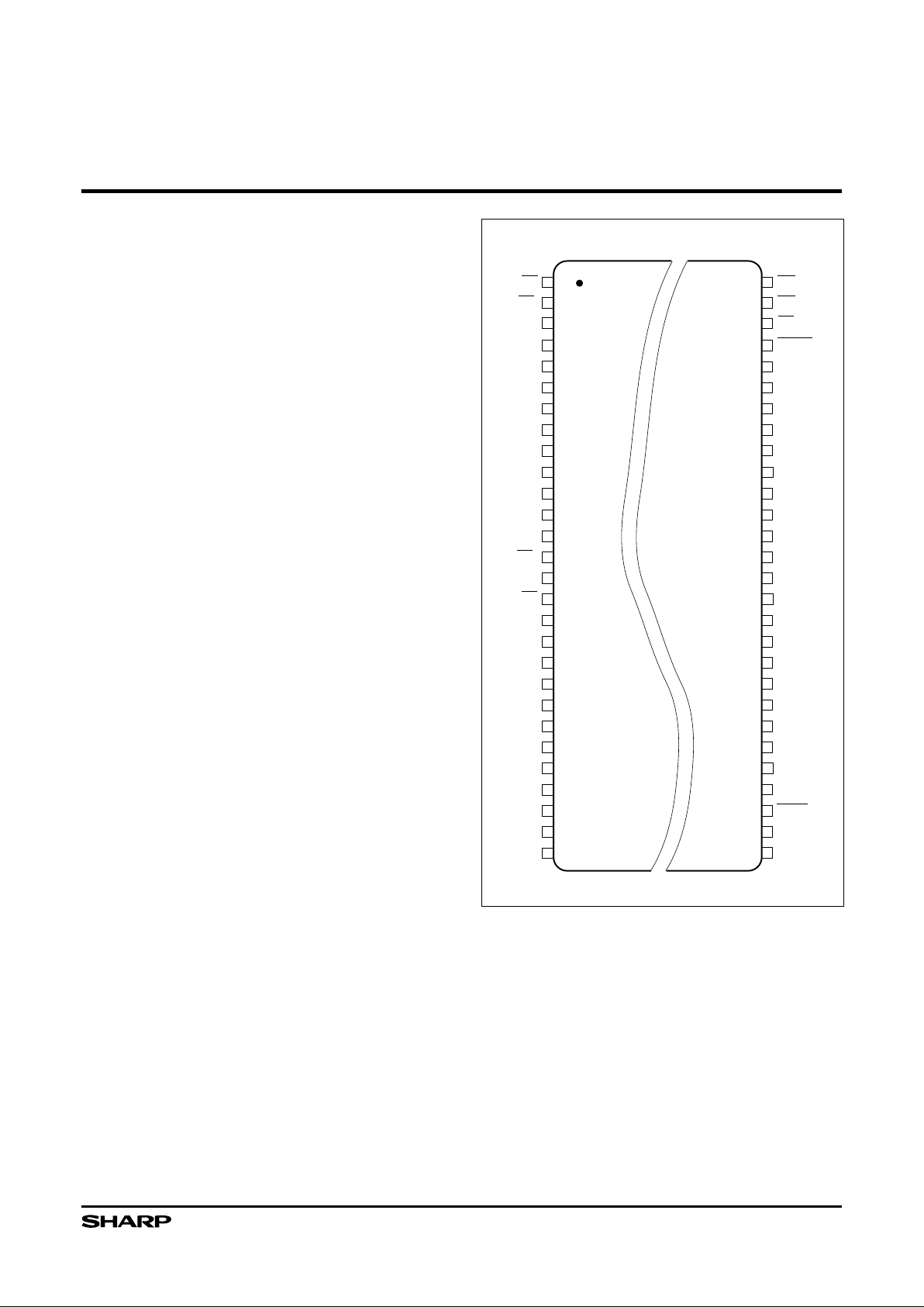
Figure 1. TSOP Configuration
FEATURES
• User-Configurable x8 or x16 Operation
• User-Selectable 3.3 V or 5 V V
CC
• 70 ns Maximum Access Time
• 0.32 MB/sec Write Transf er Rate
• 100,000 Erase Cycles per Block
• 32 Independently Lockable Blocks
• 5 V Write/Erase Operation (5 V V
PP
)
– No Requirement for DC/DC Converter
to Write/Erase
• Minimum 2.7 V Read capability
– 160 ns Maximum Access Time
(V
CC
= 2.7 V)
• Revolutionary Architecture
– Pipelined Command Execution
– Write During Erase
– Command Superset of
Sharp LH28F008SA
• 5 µA (Typ.) I
CC
in CMOS Standby
• 1 µA (Typ.) Deep Power-Down
• State-of-the-Art 0.55 µm ETOX™
Flash Technology
• 56-Pin, 1.2 mm × 14 mm × 20 mm
TSOP (Type I) Package
28F016SUT-1
TOP VIEW56-PIN TSOP
2
3
4
5
8
9
A
16
A
19
A
20
53
52
51
50
49
48
45
42
NC
6
7A
17
A
18
47
46
RY/BY
DQ
15
DQ
14
GND
GND
10
11
12
55
54 OE
V
CC
13 44 DQ
4
43 V
CC
A
15
DQ
7
14
15
16
17
18
19
20
39
36
41
40
38
37
DQ
3
DQ
10
DQ
2
V
CC
A
10
A
9
A
11
V
PP
RP
CE
0
A
8
DQ
9
WE
DQ
6
DQ
13
DQ
11
56
1
CE
1
3/5
WP
21
22
23
24
25
26
27
28
A
4
A
3
A
5
A
7
A
6
GND
A
2
A
1
34 DQ
8
35 DQ
1
31
33
32
30
29
A
0
BYTE
NC
NC
DQ
0
A
14
A
13
A
12
DQ
5
DQ
12
Page 2
LH28F016SU 16M (1M × 16, 2M × 8) Flash Memory
2
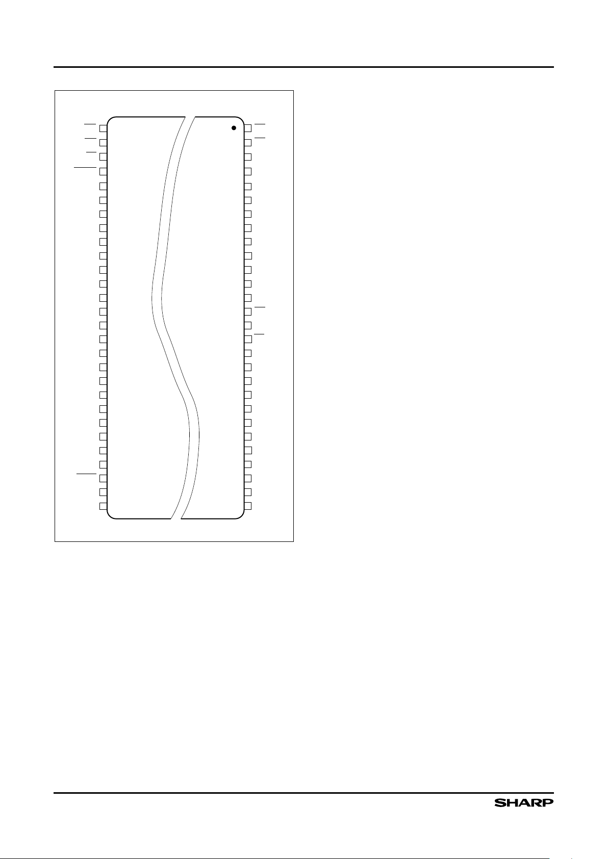
Figure 2. TSOP Reverse Bend Configuration
INTRODUCTION
Sharp’s LH28F016SU 16M Flash Memory is a revolutionary architecture which enables the design of truly
mobile, high performance, personal computing and communication products. With innovative capabilities, 5 V
single voltage operation and very high read/write performance, the LH28F016SU is also the ideal choice for
designing embedded mass storage memory systems.
The LH28F016SU is a very high density , highest performance non-volatile read/write solution for solid-state
storage applications. Its symmetrically blocked architecture (100% compatible with the LH28F008SA 8M
Flash memory), extended cycling, low power 3.3 V
operation, very fast write and read performance and
selective bloc k locking provide a highly fle xible memory
component suitable for high density memory cards,
Resident Flash Arrays and PCMCIA-ATA Flash Drives.
The LH28F016SU’s dual read voltage enables the
design of memory cards which can interchangeably be
read/written in 3.3 V and 5.0 V systems. Its x8/x16
architecture allows the optimization of memory to processor interface. The flexible block locking option
enables bundling of executable application software in
a Resident Flash Array or memory card. Manuf actured
on Sharp’s 0.55 µm ETOX™ process technology, the
LH28F016SU is the most cost-effective, high-density
3.3 V flash memory.
DESCRIPTION
The LH28F016SU is a high performance 16M
(16,777,216 bit) block erasable non-volatile random
access memory organized as either 1M × 16 or 2M × 8.
The LH28F016SU includes thirty-two 64K (65,536)
blocks or thirty-two 32-KW (32,768) blocks. A chip
memory map is shown in Figure 4.
The implementation of a new architecture, with many
enhanced features, will improve the device operating
characteristics and results in greater product reliability
and ease of use.
Among the significant enhancements of the
LH28F016SU:
• 5 V Write/Erase Operation (5 V V
PP
)
• 3.3 V Low Power Capability (2.7 V V
CC
Read)
• Improved Write P erformance
• Dedicated Block Write/Erase Protection
A 3/5» input pin reconfigures the device internally for
optimized 3.3 V or 5.0 V read/write operation.
The LH28F016SU will be available in a 56-pin,
1.2 mm thick × 14 mm × 20 mm TSOP (Type I) package. This f orm factor and pinout allow for v ery high board
layout densities.
28F016SUT-17
TOP VIEW56-PIN TSOP
2
3
4
5
89A
16
A
19
A
20
53
52
51
50
49
48
45
42
NC
6
7A
17
A
18
47
46
DQ
15
DQ
14
GND
GND
10
11
12
55
54OE
V
CC
1344DQ
4
43V
CC
A
15
DQ
7
14
15
16
17
18
19
20
39
36
41
40
38
37
DQ
3
DQ
10
DQ
2
V
CC
A
10
A
9
A
11
V
PP
RP
CE
0
A
8
DQ
9
WE
DQ
6
DQ
13
DQ
11
56
1
CE
1
3/5
WP
21
22
23
24
25
26
27
28
A
4
A
3
A
5
A
7
A
6
GND
A
2
A
1
34DQ
8
35DQ
1
31
33
32
30
29
A
0
BYTE
NC
NC
DQ
0
A
14
A
13
A
12
DQ
5
DQ
12
RY/BY
Page 3
16M (1M × 16, 2M × 8) Flash Memory LH28F016SU
3
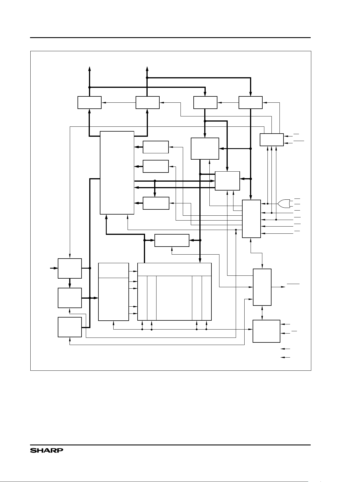
Figure 3. LH28F016SU Block Diagram (Architectural Evolution Includes Page Buffers,
Queue Registers and Extended Status Registers)
OUTPUT
BUFFER
OUTPUT
BUFFER
INPUT
BUFFER
INPUT
BUFFER
DQ8 - DQ
15
DQ0 - DQ
7
ID
REGISTER
OUTPUT
MULTIPLEXER
CSR
ESRs
DATA
COMPARATOR
DATA
QUEUE
REGISTERS
PAGE
BUFFERS
I/O
LOGIC
CUI
WSM
64KB BLOCK 0
64KB BLOCK 1
64KB BLOCK 30
64KB BLOCK 31
. . .
. . .
Y GATING/SENSING
Y-DECODER
X-DECODER
CE
0
CE
1
OE
WE
WP
RP
PROGRAM/
ERASE
VOLTAGE
SWITCH
3/5
BYTE
V
PP
3/5
V
CC
GND
RY/BY
ADDRESS
COUNTER
ADDRESS
QUEUE
LATCHES
INPUT
BUFFER
A0 - A
20
. . .
28F016SUT-2
Page 4
LH28F016SU 16M (1M × 16, 2M × 8) Flash Memory
4
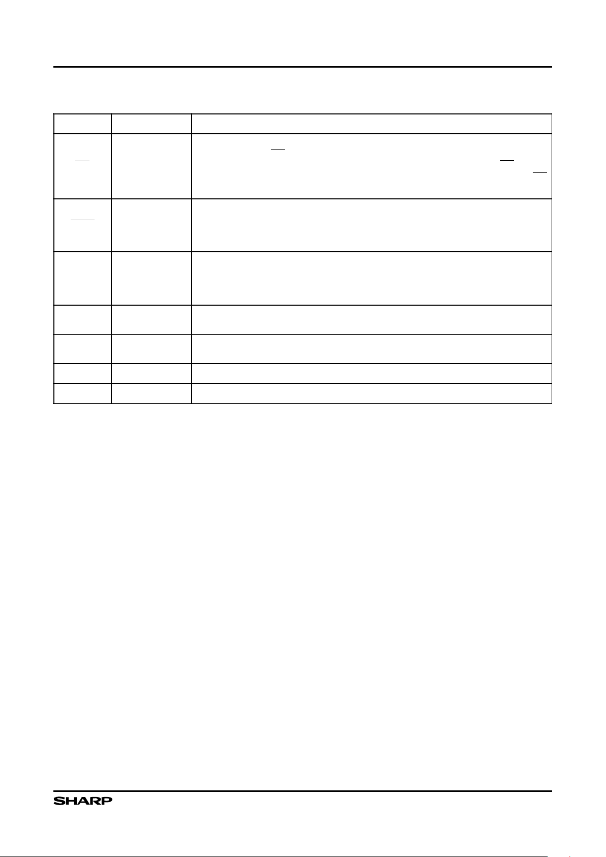
PIN DESCRIPTION
SYMBOL TYPE NAME AND FUNCTION
A
0
INPUT
BYTE-SELECT ADDRESS: Selects between high and low byte when device is in x8
mode. This address is latched in x8 Data Writes. Not used in x16 mode (i.e., the A
0
input buffer is turned off when BYTE is high).
A
1
- A
15
INPUT
WORD-SELECT ADDRESSES: Select a word within one 64K block. A
6
- A
15
selects
1 of 1024 rows, and A1 - A5 selects 16 of 512 columns. These addresses are
latched during Data Writes.
A
16
- A
20
INPUT
BLOCK-SELECT ADDRESSES: Select 1 of 32 Erase blocks. These addresses are
latched during Data Writes, Erase and Lock-Block operations.
DQ
0
- DQ7INPUT/OUTPUT
LOW-BYTE DATA BUS: Inputs data and commands during CUI write cycles.
Outputs array, buffer, identifier or status data in the appropriate Read mode. Floated
when the chip is de-selected or the outputs are disabled.
DQ
8
- DQ15INPUT/OUTPUT
HIGH-BYTE DATA BUS: Inputs data during x16 Data-Write operations. Outputs
array, buffer or identifier data in the appropriate Read mode; not used for Status
register reads. Floated when the chip is de-selected or the outputs are disabled.
CE
»
0
, CE
»
1
INPUT
CHIP ENABLE INPUTS: Activate the device’s control logic, input buffers, decoders and
sense amplifiers. With either CE
»
0
or CE
»
1
high, the device is de-selected and power
consumption reduces to Standby levels upon completion of any current Data-Write or
Erase operations. Both CE
»
0
, CE
»
1
must be low to select the device. All timing
specifications are the same for both signals. Device Selection
occ
urs with the latter
falling edge of CE
»
0
or CE
»
1
. The first rising edge of CE
»
0
or CE
»
1
disables the device.
RP
»
INPUT
RESET/POWER-DOWN: With RP
»
low, the device is reset, any current operation is
aborted and device is put into the deep power down mode. When the power is
turned on, RP
»
pin is turned to low in order to return the device to default con-
figuration. When the 3/5
»
pin is switched, or when the power transition is occurred, or
at the power on/off, RP
»
is required to stay low in order to pr otect data from noise.
When returning from Deep Power-Down, a recovery time of 400
ns
(V
CC
+5.0 V ±0.5 V) is required to allow these circuits to power-up. When RP
» goes
low, any current or pending WSM operation(s) are terminated, and the device is
reset. All Status registers return to ready (with all status flags cleared). After
returning, the device is in read array mode.
OE
» INPUT
OUTPUT ENABLE: Gates device data through the output buffers when low. The
outputs float to tri-state off when OE
» is high.
NOTE:
CE
»
X
overrides OE
»
, and OE
»
overrides WE.
WE INPUT
WRITE ENABLE: Controls access to the CUI, Page Buffers, Data Queue Registers
and Address Queue Latches. WE is active low, and latches both address and data
(command or array) on its rising edge.
RY
»/BY
»
OPEN DRAIN
OUTPUT
READY/BUSY: Indicates status of the internal WSM. When low, it ind icates that the
WSM is busy performing an operation. RY/BY# high indicates that the WSM is ready
for new operations (or WSM has completed all pending operations), or Erase is
Suspended, or the device is in deep power-down mode. This output is always active
(i.e., not floated to tri-state off when OE
»
or CE
»
0
, CE
»
1
are high), except if a RY
»
/BY
»
Pin Disable command is issued.
Page 5
16M (1M × 16, 2M × 8) Flash Memory LH28F016SU
5
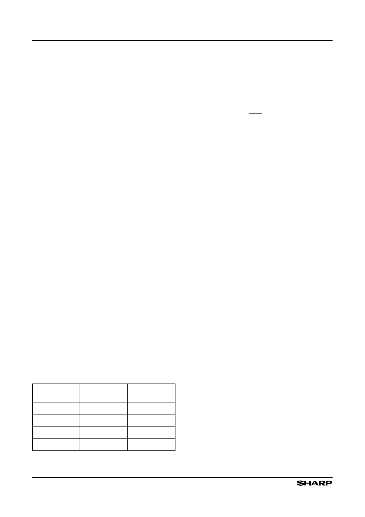
PIN DESCRIPTION (Continued)
SYMBOL TYPE NAME AND FUNCTION
WP INPUT
WRITE PROTECT: Erase blocks can be locked by writing a non-volatile lock-bit for
each block. When WP is low, those locke d blocks as reflected by the B lock-Lock Status
bits (BSR.6), are protected from inadvertent Data Writes or Erases. When WP is high,
all blocks can be Written or Erased regardless of the state of the lock-bits. The WP
input buffer is disabled when RP
» transitions low (deep power-down mode).
BYTE INPUT
BYTE ENABLE: BYTE low places device x8 mode. All data is then input or output
on DQ
0
- DQ7, and DQ
8
- DQ15 float. Address A0 selects between the high and low
byte. BYTE high places the device in x16 mode, and turns off the A0 input buffer.
Address A1, then becomes the lowest order address.
3/5
» INPUT
3.3/5.0 V OLT SELECT: 3/5
» high configures internal circuit s for 3.3 V operation. 3/5
»
low configures internal circuits f or 5.0 V operation.
NOTES:
Reading the array with 3/5
» high in a 5.0 V system could damage the
device. There is a significant delay from 3/5
» switching to valid data.
V
PP
SUPPLY
ERASE/WRITE POWER SUPPLY: For erasing memory array blocks or writing
words/bytes/pages into the flash array.
V
CC
SUPPLY
DEVICE POWER SUPPLY (3.3 V ±0.3 V, 5.0 V ±0.5 V) (2.7 V ~ 3.6 V at Read
Operation)
: Do not leave any power pins floating.
GND SUPPLY
GROUND FOR ALL INTERNAL CIRCUITRY: Do not leave any ground pins floating.
NC
NO CONNECT: No internal connection to die, lead may be driven or left floating.
The LH28F016SU incorporates two Page Buffers of
256 Bytes (128 W ords) each to allow page data writes.
This feature can improve a system write performance
over pre vious flash memory devices.
All operations are started by a sequence of Wr ite
commands to the device. Three Status Registers
(described in detail later) and a RY»/BY» output pin
provide information on the progress of the requested
operation.
While the LH28F008SA requires an operation to complete before the next operation can be requested, the
LH28F016SU allows queuing of the next operation while
the memory executes the current operation. This eliminates system overhead when writing sev eral b ytes in a
row to the array or erasing several blocks at the same
time. The LH2F016SUR-10 can also perform write operations to one block of memory while performing erase
of another block.
The LH28F016SU provides user-selectable block
locking to protect code or data such as Device Driv ers,
PCMCIA card information, ROM-Executable O/S or
Application Code. Each block has an associated nonvolatile lock-bit which determines the lock status of the
block. In addition, the LH28F016SU has a master Write
Protect pin (WP
»
) which prevents any modifications to
memory blocks whose lock-bits are set.
A Command User Interface (CUI) serves as the system interface between the microprocessor or
microcontroller and the internal memory operation.
Internal Algorithm Automation allows Byte/Word
Writes and Block Erase operations to be executed
using a Two-Write command sequence to the CUI in
the same way as the LH28F008SA 8M Flash memory.
A Superset of commands have been added to the
basic LH28F008SA command-set to achieve higher
write performance and provide additional capabilities.
These new commands and features include:
• Page Buffer Writes to Flash
• Command Queuing Capability
• Automatic Data Writes During Erase
• Software Locking of Memory Blocks
• T w o-Byte Successive Writes in 8-bit Systems
• Erase All Unlocked Blocks
Writing of memory data is performed in either byte or
word increments typically within 8 µs, a 25% improvement over the LH28F008SA. A Block Erase operation
erases one of the 32 blocks in typically 0.7 seconds,
independent of the other blocks, which is about 55%
improvement ov er the LH28F008SA.
Page 6
LH28F016SU 16M (1M × 16, 2M × 8) Flash Memory
6
OPERATING
TEMPERATURE
V
CC
SUPPLY
MAX. ACCESS
(T
ACC
)
0 - 70°C 4.75 - 5.25 V 70 ns
0 - 70°C 4.5 - 5.5 V 80 ns
0 - 70°C 3.0 - 3.6 V 120 ns
0 - 70°C 2.7 - 3.6 V 160 ns
The LH28F016SU contains three types of Status
Registers to accomplish various functions:
• A Compatible Status Register (CSR) which is 100%
compatible with the LH28F008SA Flash memory’s
Status Register. This register , when used alone, pro-
vides a straightforward upgrade capability to the
LH28F016SU from a LH28F008SA based design.
• A Global Status Register (GSR) which informs the
system of command Queue status, Page Buff er sta-
tus, and over all Write State Machine (WSM) status.
• 32 Block Status Registers (BSRs) which provide
block-specific status inf ormation such as the bloc k
lock-bit status.
The GSR and BSR memory maps for Byte-Wide and
Word-Wide modes are shown in Figures 5 and 6.
The LH28F016SU incorporates an open drain
RY»/BY» output pin. This feature allows the user to ORtie many RY »/BY» pins together in a multiple memory configuration such as a Resident Flash Array.
The LH28F016SU also incorporates a dual chipenable function with two input pins, CE »0 and CE»1. These
pins have exactly the same functionality as the regular
chip-enable pin CE» on the LH28F008SA. F or minimum
chip designs, CE»1 may be tied to ground and use CE»
0
as the chip enable input. The LH28F016SU uses the
logical combination of these two signals to enable or
disable the entire chip. Both CE»0 and CE»1 must be active low to enable the de vice and if either one becomes
inactive, the chip will be disabled. This feature, along
with the open drain RY »/BY» pin, allows the 0system designer to reduce the number of control pins used in a
large array of 16M de vices .
The BY»TE» pin allo ws either x8 or x16 read/writes to
the LH28F016SU. BY»TE» at logic low selects 8-bit mode
with address A0 selecting between low byte and high
byte. On the other hand, BY»TE» at logic high enables
16-bit operation with address A1 becoming the lowest
order address and address A0 is not used (don’t care).
A block diagram is shown in Figure 3.
The LH28F016SU is specified for a maximum
access time of each version, as follows:
The LH28F016SU incorporates an Automatic Pow er
Saving (APS) feature which substantially reduces the
active current when the device is in static mode of
operation (addresses not switching).
In APS mode, the typical I
CC
current is 2 mA at 5.0 V
(1 mA at 3.3 V).
A Deep Power-Down mode of operation is invoked
when the RP» (called PWD on the LH28F008SA) pin
transitions low , any current operation is aborted and the
device is put into the deep power-do wn mode. This mode
brings the device power consumption to less than 5 µA
typically, and provides additional write protection by
acting as a device reset pin during power transitions.
When the power is turned on, RP» pin turned to low order to return the device to default configuration. When
the 3/5» pin is switched, or when the pow er transition is
occured, or at the power on/off, RP» is required to stay
low in order to protect data from noise. A recov ery time
of 550 ns (V
CC
= 5.0 V ± 0.5 V ) is required from RP»
switching high until outputs are again valid. In the Deep
Power-Down state, the WSM is reset (any current
operation will abort) and the CSR, GSR and BSR registers are cleared.
A CMOS Standby mode of operation is enabled when
either CE»0 or CE»1 transitions high and RP» stays high
with all input control pins at CMOS levels . In this mode ,
the device typically draws an I
CC
standby current of
10 µA.
Page 7
16M (1M × 16, 2M × 8) Flash Memory LH28F016SU
7
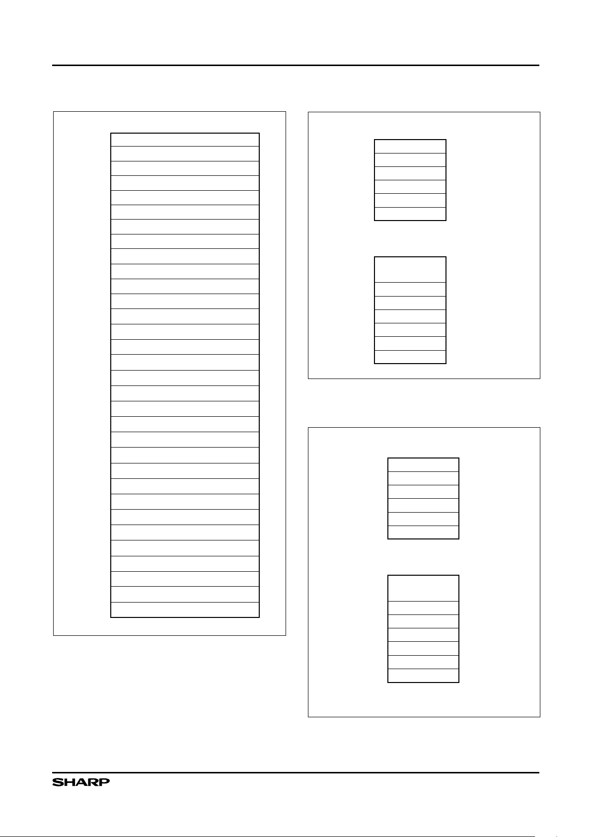
Figure 4. LH28F016SU Memory Map
(Byte-Wide Mode)
MEMORY MAP
Figure 5. Extended Status Register
Memory Map (Byte-Wide Mode)
Figure 6. Extended Status Register
Memory Map (Word-Wide Mode)
Extended Status Registers Memory Map
RESERVED
GSR
RESERVED
BSR31
RESERVED
RESERVED
F8003H
F8002H
F8001H
F8000H
A[20:1] (NOTE)
x16 MODE
.
.
.
RESERVED
GSR
RESERVED
BSR0
RESERVED
RESERVED
00003H
00002H
00001H
00000H
RESERVED
08001H
28F016SUT-5
NOTE: In word-wide mode A0 don't care, address values
are ignored A0.
15
1F0000H
1FFFFFH
1EFFFFH
1E0000H
1DFFFFH
1D0000H
1CFFFFH
1C0000H
1BFFFFH
1B0000H
1AFFFFH
1A0000H
19FFFFH
190000H
18FFFFH
180000H
17FFFFH
170000H
16FFFFH
160000H
15FFFFH
150000H
14FFFFH
140000H
13FFFFH
130000H
12FFFFH
120000H
11FFFFH
110000H
10FFFFH
100000H
0FFFFFH
0F0000H
0EFFFFH
0E0000H
0DFFFFH
0D0000H
0CFFFFH
0C0000H
0BFFFFH
0B0000H
0AFFFFH
0A0000H
09FFFFH
090000H
08FFFFH
080000H
07FFFFH
070000H
06FFFFH
060000H
05FFFFH
050000H
04FFFFH
040000H
03FFFFH
030000H
02FFFFH
020000H
01FFFFH
010000H
00FFFFH
000000H
14
13
12
11
10
9
8
7
6
5
4
3
2
0
64KB BLOCK
16 64KB BLOCK
17 64KB BLOCK
18 64KB BLOCK
19 64KB BLOCK
20 64KB BLOCK
21 64KB BLOCK
22 64KB BLOCK
23 64KB BLOCK
24 64KB BLOCK
25 64KB BLOCK
26 64KB BLOCK
27 64KB BLOCK
28 64KB BLOCK
29 64KB BLOCK
30
64KB BLOCK
31 64KB BLOCK
64KB BLOCK
64KB BLOCK
64KB BLOCK
64KB BLOCK
64KB BLOCK
64KB BLOCK
64KB BLOCK
64KB BLOCK
64KB BLOCK
64KB BLOCK
64KB BLOCK
64KB BLOCK
64KB BLOCK
1
64KB BLOCK
64KB BLOCK
28F016SUT-3
RESERVED
GSR
RESERVED
BSR31
RESERVED
RESERVED
1F0006H
1F0005H
1F0004H
1F0003H
1F0002H
1F0001H
1F0000H
A[20:0]
x8 MODE
.
.
.
RESERVED
GSR
RESERVED
BSR0
RESERVED
RESERVED
000006H
000005H
000004H
000003H
000002H
000001H
000000H
RESERVED
010002H
28F016SUT-4
Page 8
LH28F016SU 16M (1M × 16, 2M × 8) Flash Memory
8
BUS OPERATIONS, COMMANDS AND STATUS REGISTER DEFINITIONS
Bus Operations for Word-Wide Mode (BY»TE» = VIH)
MODE RP
» CE »
1
CE
»
0
OE
» WE A
1
DQ0 - DQ
15
RY
»/BY » NOTE
Read V
IH
V
IL
V
IL
V
IL
V
IH
XD
OUT
X1, 2, 7
Output Disable V
IH
V
IL
V
IL
V
IH
V
IH
X High-Z X 1, 6, 7
Standby V
IH
V
IL
V
IH
V
IH
V
IH
V
IL
V
IH
X X X High-Z X 1, 6, 7
Deep Powe r-Down V
IL
XXXXX High-Z VOH1, 3
Manufacturer ID V
IH
V
IL
V
IL
V
IL
V
IH
V
IL
00B0H V
OH
4
Device ID V
IH
V
IL
V
IL
V
IL
V
IH
V
IH
6688H V
OH
4
Writ e V
IH
V
IL
V
IL
V
IH
V
IL
XDINX1, 5, 6
NOTES:
1. X can be VIH or VIL for address or control pins except for RY»/BY», which is either VOL or VOH.
2. RY»/BY» output is open drain. When the WSM is ready, Erase is suspended or the device is in deep power-down mode,
RY»/BY» will be at VOH if it is tied to VCC through a resistor. When the RY»/BY» at VOH is independent of OE
»
while a WSM
operation is in progress.
3. RP» at GND ± 0.2 V ensures the lowest deep power-down current.
4. A0 and A1 at VIL provide manufacturer ID codes in x8 and x16 modes respectively. A0 and A1, at VIH provide device ID
codes in x8 and x16 modes respectively. All other addresses are set to zero.
5. Commands for different Erase operations, Data Write operations of Lock-Block operations can only be successfully
completed when VPP = V
PPH
.
6. While the WSM is running, RY»/BY» in Level-Mode (default) stays at VOL until all operations are complete. RY»/BY» goes to
VOH when the WSM is not busy or in erase suspend mode.
7. RY»/BY» may be at VOL while the WSM is busy performing various operations. For example, a status register read during a
write operations.
Bus Operations For Byte-Wide Mode (BY»TE» = VIL)
MODE RP
» CE »
1
CE
»
0
OE
» WE A
0
DQ0 - DQ
7
RY
»/BY » NOTE
Read V
IH
V
IL
V
IL
V
IL
V
IH
XD
OUT
X1, 2, 7
Output Disable V
IH
V
IL
V
IL
V
IH
V
IH
X High-Z X 1, 6, 7
Standby V
IH
V
IL
V
IH
V
IH
V
IH
V
IL
V
IH
X X X High-Z X 1, 6, 7
Deep Powe r-Down V
IL
XXXXX High-Z VOH1, 3
Manufacturer ID V
IH
V
IL
V
IL
V
IL
V
IH
V
IL
B0H V
OH
4
Device ID V
IH
V
IL
V
IL
V
IL
V
IH
V
IH
88H V
OH
4
Writ e V
IH
V
IL
V
IL
V
IH
V
IL
XDINX1, 5, 6
Page 9
16M (1M × 16, 2M × 8) Flash Memory LH28F016SU
9
COMMAND
FIRST BUS CYCLE SECOND BUS CYCLE
NOTE
OPER. ADDRESS DATA OPER. ADDRESS DATA
Read Array Write X FFH Read AA AD
Intelligent Identifier Write X 90H Read IA ID 1
Read Compatible Status Register Write X 70H Read X CSRD 2
Clear Status Register Write X 50H 3
Word Write Write X 4 0H Wr ite WA WD
Alternate Word/Byte Write Write X 10H Write WA WD
Block Erase/Confirm Write X 20H Write BA D0H
Erase Suspend/Resume Write X B0H Write X D0H
ADDRESS DATA
AA = Array Address AD = Array Data
BA = Block Address CSRD = CSR Data
IA = Identifier Address ID = Identifier Data
WA = Write Address WD = Write Data
X = Don’t Care
NOTES:
1. Following the intelligent identifier command, two Read operations access the manufacturer and device signature codes.
2. The CSR is automatically available after device enters Data Write, Erase or Suspend operations.
3. Clears CSR.3, CSR.4, and CSR.5. Also clears GSR.5 an all BSR.5 and BSR.2 bits. See Status register definitions.
LH28F008SA-Compatible Mode Command Bus Definitions
Page 10
LH28F016SU 16M (1M × 16, 2M × 8) Flash Memory
10
LH28F016SU Performance Enhancement Command Bus Definitions
COMMAND MODE
FIRST BUS CYCLE SECOND BUS CYCLE THIRD BUS CYCLE
NOTE
OPER. ADDR. DAT A OPE R. ADDR. DAT A OPE R. ADDR. DATA
Read Extended
Status Register
Write X 71H Read RA
GSRD
BSRD
1
Page Buffer Swap Write X 72H 7
Read Page Buffer Write X 75H Read PA PD
Single Load to
Page Buffer
Writ e X 74H Wri te PA PD
Sequential Load to
Page Buffer
x8 Wr ite X E0 H Writ e X BCL Writ e X BCH 4 , 6, 1 0
x16 Writ e X E 0H Wri te X WCL Write X WCH
4, 5,
6, 10
Page Buffer Write
to Flash
x8 Write X 0CH Write A0
BC
(L, H)
Write WA BC (H, L)
3, 4,
9, 10
x16 Writ e X 0 CH Writ e X WCL Write WA WCH 4, 5, 10
Two-Byte Wri te x8 Write X FBH Write A0
WD
(L, H)
Write WA WD (H , L) 3
Block
Erase/Confirm
Write X 20H Write BA D0H
Lock Block/Confirm Write X 77H Write BA D0H
Upload Status
Bits/Confirm
Writ e X 9 7 H Wr i te X D0H 2
Uploa d Devic e
Information
Writ e X 9 9H Wr i te X D0 H
Erase All Unlocked
Blocks/Confirm
Writ e X A7H Wr i t e X D0 H
RY
»/BY » Enable to
Level-Mode
Write X 96H Write X 01H 8
RY
»/BY » Pulse-On-
Writ e
Write X 96H Write X 02H 8
RY
»
/BY
»
Pulse-On-
Erase
Write X 96H Write X 03H 8
RY
»/BY » Disable Write X 96H Write X 04H 8
Sleep Write X F0H
Abort Write X 80H
ADDRESS DATA
BA = Block Address AD = Array Data
PA = Page Buffer Address PD = Page Buffer Data
RA = Extended Register Address BSRD = BSR Data
WA = Write Address GSRD = GSR Data
X = Don’t Care WC (L, H) = Word Count (Low, High)
BC (L, H) = Byte Count (Low, High)
WD (L, H) = Write Data (Low, High)
Page 11
16M (1M × 16, 2M × 8) Flash Memory LH28F016SU
11
NOTES:
1. RA can be the GSR address or any BSR address. See Figure 5 and 6 for Extended Status Register Memory Maps.
2. Upon device power-up, all BSR lock-bits come up locked. The Uploaded Status Bits command must be written to reflect the
actual lock-bit status.
3. A0 is automatically complemented to load second byte of data. BY» TE» must be at VIL. A0 value determines which WD/BC is supplied
first: A0 = 0 looks at the WDL/BCL, A0 = 1 looks at the WDH/BCH.
4. BCH/WCH must be at 00H for this product because of the 256-Byte (128 Word) Page Buffer size and to avoid writing the Page Buffer
contents into more than one 256-Byte segment within an array block. They are simply shown for future Page Buffer expandability.
5. In x16 mode, only the lower byte DQ0 - DQ7 is used for WCL and WCH. The upper byte DQ8 - DQ15 is a don’t care.
6. PA and PD (Whose count is given in cycles 2 and 3) are supplied starting in the 4th cycle which is not shown.
7. This command allows the user to swap between available Page Buffers (0 or 1).
8. These commands reconfigure RY»/BY» output to one of two pulse-modes or enable and disable the RY »/BY» function.
9. Write address, WA, is the Destination address in the flash array which must match the Source address in the Page Buffer. Refer to the
LH28F016SU User’s Manual.
10. BCL = 00H corresponds to a Byte count of 1. Similarly, WCL = 00H corresponds to a Word count of 1.
WSMS ESS ES DWS VPPS R R R
76543210
CSR.7 = WRITE STATE MACHINE STATUS (WSMS)
1 = Ready
0 = Busy
CSR.6 = ERASE-SUSPEND STATUS (ESS)
1 = Erase Suspended
0 = Erase in Progress/Completed
CSR.5 = ERASE STATUS (ES)
1 = Error in Block Erasure
0 = Successful Block Erase
CSR.4 = DATA-WRITE STATUS (DWS)
1 = Error in Data Write
0 = Data Write Successful
CSR.3 = VPP STATUS (VPPS)
1 = VPP Low Detect, Operation Abort
0 = VPP OK
NOTES:
1. RY»/BY» output or WSMS bit must be checked to determine
completion of an operation (Erase Suspend, Erase or Data
Write) before the appropriate Status bit (ESS, ES or DWS)
is checked for success.
2. If DWS and ES are set to ‘1’ during an erase attempt, an
improper command sequence was entered. Clear the CSR
and attempt the operation again.
3. The VPPS bit, unlike an A/D converter, does not provide
continuous indication of VPP level. The WSM interrogates
VPP’s level only after the Data-Write or Erase command
sequences have been entered, and informs the system if
VPP has not been switched on. VPPS is not guaranteed to
report accurate feedback between V
PPL
and V
PPH
.
4. CSR.2 - CSR.0 = Reserved for future enhancements.
These bits are reserved for future use and should be
masked out when polling the CSR.
Compatible Status Register
Page 12
LH28F016SU 16M (1M × 16, 2M × 8) Flash Memory
12
WSMS OSS DOS DSS QS PBAS PBS PBSS
76543210
GSR.7 = WRITE STATE MACHINE STATUS (WSMS)
1 = Ready
0 = Busy
GSR.6 = OPERATION SUSPEND STATUS (OSS)
1 = Operation Suspended
0 = Operation in Progress/Completed
GSR.5 = DEVICE OPERATION STATUS (DOS)
1 = Operation Unsuccessful
0 = Operation Successful or Currently Running
GSR.4 = DEVICE SLEEP STATUS(DSS)
1 = Device in Sleep
0 = Device Not in Sleep
MATRIX 5/4
00 = Operation Successful or currently Running
01 = Device in Sleep Mode or Pending Sleep
10 = Operation Unsuccesful
11 = Operation Unsuccessful or Aborted
GSR.3 = QUEUE STATUS (QS)
1 = Queue Full
0 = Queue Available
GSR.2 = PAGE BUFFER AVAILABLE STATUS (PBAS)
1 = One or Two Page Buffers Available
0 = No Page Buffer Available
GSR.1 = PAGE BUFFER STATUS (PBS)
1 = Selected Page Buffer Ready
0 = Selected Page Buffer Busy
GSR.0 = PAGE BUFFER SELECT STATUS (PBSS)
1 = Page Buffer 1 Selected
0 = Page buffer 0 Selected
NOTES:
1. RY»/BY» output or WSMS bit must be checked to determine
completion of an operation (Block Lock, Suspend, any
RY»/BY» reconfiguration, Upload Status Bits, Erase or Data
Write) before the appropriate Status bit (OSS or DOS) is
checked for success.
2. If operation currently running, then GSR.7 = 0.
3. If device pending sleep, then GSR.7 = 0.
4. Operation aborted: Unsucccessful due to Abort command.
5. The device contains two Page Buffers.
6. Selected Page Buffer is currently busy with WSM operation.
7. When multiple operations are queued, checking BSR.7
only provides indication of completion for that particular
block. GSR.7 provides indication when all queuedf operations are completed.
GLOBAL STATUS REGISTER
Page 13

16M (1M × 16, 2M × 8) Flash Memory LH28F016SU
13
BS BLS BOS BOAS QS VPPS R R
76543210
BSR.7 = BLOCK STATUS (BS)
1 = Ready
0 = Busy
BSR.6 = BLOCK-LOCK STATUS (BLS)
1 = Block Unlocked for Write/Erase
0 = Block Locked for Write/Erase
BSR.5 = BLOCK OPERATION STATUS (BOS)
1 = Operation Unsuccessful
0 = Operation Successful or Currently Running
BSR.4 = BLOCK OPERATION ABORT STATUS (BOAS)
1 = Operation Aborted
0 = Operation Not Aborted
MATRIX 5/4
00 = Operation Successful or Currently Running
01 = Not a valid Combination
10 = Operation Unsuccessful
11 = Operation Aborted
BSR.3 = QUEUE STATUS (QS)
1 = Queue Full
0 = Queue Available
BSR.2 = V
PP
STATUS (V
PPS
)
1 = V
PP
Low Detect, Operation Abort
0 = V
PP
OK
NOTES:
1. RY»/BY» output or BS bit must be checked to determine
completion of an operation (Block Lock, Suspend, Erase or
Data Write) before the appropriate Status bits (BOS, BLS)
is checked for success.
2. The BOAS bit will not be set until BSR.7 = 1.
3. Operation halted via Abort command.
4. BSR.1-0 = Reserved for future enhancements. These bits
are reserved for future use; mask them out when polling
the BSRs.
5. When multiple operations are queued, checking BSR.7
only provides indication of completion for that particular
block. GSR.7 provides indication when all queued operations are completed.
BLOCK STATUS REGISTER
Page 14

LH28F016SU 16M (1M × 16, 2M × 8) Flash Memory
14
*
WARNING: Stressing the device beyond the “Absolute Maximum Ratings” may cause permanent damage. These are stress ratings only. Operation beyond
the “Operating Conditions” is not recommended and
extended e xposure beyond the “Operating Conditions”
may affect device reliability.
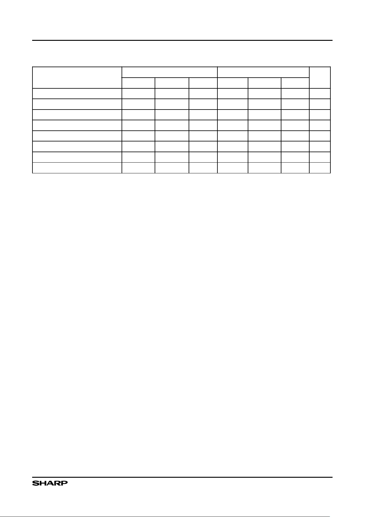
ELECTRICAL SPECIFICATIONS
Absolute Maximum Ratings*
Temperature under bias ......................... 0°C to +80°C
Storage temperature .........................-65°C to +125°C
V
CC
= 3.3 V ± 0.3 V Systems
4
SYMBOL PARAMETER MIN. MAX. UNITS TEST CONDITIONS NOTE
T
A
Operating Temperature, Commercial 0 70 °C Ambient Temperature 1
V
CC
VCC with Respect to GND -0.2 7.0 V 2
V
PP
VPP Supply Voltage with Respect to GND -0.2 7.0 V 2
V
Voltage on any Pin (Except VCC, VPP)
with Respe ct t o GN D
-0.5 VCC + 0.5 V 2
I Current into any Non-Supply Pin ±30 mA
I
OUT
Output Short Circuit Current 100.0 mA 3
V
CC
= 5.0 V ± 0.5 V Systems
4
SYMBOL PARAMETER MIN. MAX. UNITS TEST CONDITIONS NOTE
T
A
Operating Temperature, Commercial 0 70 °C Ambient Temperature 1
V
CC
VCC with Respect to GND -0.2 7.0 V 2
V
PP
VPP Supply Voltage with Respect to GND -0.2 7.0 V 2
V
Voltage on any Pin (Except VCC, VPP)
with Respe ct t o GN D
-0.5 7.0 V 2
I Current into any Non-Supply Pin ±30 mA
I
OUT
Output Short Circuit Current 100.0 mA 3
NOTES:
1. Operating temperature is for commercial product defined by this specification.
2. Minimum DC voltage is -0.5 V on input/output pins. During transitions, this level may undershoot to -2.0 V for periods < 20 ns.
Maximum DC voltage on input/output pins is V
CC
+ 0.5 V which, during transitions, may overshoot to V
CC
+ 2.0 V for periods < 20 ns.
3. Output shorted for no more than one second. No more than one output shorted at a time.
4. AC specifications are valid at both voltage ranges. See DC Characteristics tables for voltage range-specific specifications.
Page 15

16M (1M × 16, 2M × 8) Flash Memory LH28F016SU
15
Capacitance
For 3.3 V Systems
SYMBOL PARAMETER TYP. MAX. UNITS TEST CONDITIONS NOTE
C
IN
Capacitance Looking into an
Address/Control Pin
68
pF TA = 25°C, f = 1.0 MHz 1
C
OUT
Capacitance Looking into an Output Pin 8 12 pF TA = 25°C, f = 1.0 MHz 1
C
LOAD
Load Capacitance Driven by Outputs for
Timing Specifications
50 pF For VCC = 3.3 V ±0.3 V 1
Equivalent Testing Load Circuit 2.5 ns 50
Ω transmission line delay
NOTE:
1. Sampled, not 100% tested.
Capacitance
For 5.0 V Systems
SYMBOL PARAMETER TYP. MAX. UNITS TEST CONDITIONS NOTE
C
IN
Capacitance Looking into an
Address/Control Pin
68
pF TA = 25°C, f = 1.0 MHz 1
C
OUT
Capacitance Looking into an Output Pin 8 12 pF TA = 25°C, f = 1.0 MHz 1
C
LOAD
Load Capacitance Driven by Outputs for
Timing Specifications
100 pF For V
CC
= 5.0 V ±0.5 V 1
Equivalent Testing Load Circuit V
CC
± 10% 2.5 ns 25 Ω transmission line delay
Equivalent Testing Load Circuit V
CC
± 5% 2.5 ns
83
Ω transmission line delay
Page 16

LH28F016SU 16M (1M × 16, 2M × 8) Flash Memory
16
Timing Nomenclature
All 3.3 V system timings are measured from where signals cross 1.5 V. F or 5.0 V systems use the standard JEDEC
crosspoint definitions. Each timing parameter consists of 5 characters. Some common e xamples are defined below:
t
CEtELQV
time (t) from CE» (E) going low (L) to the outputs (Q) becoming valid (V)
t
OEtGLQV
time (t) from OE
»
(G) going low (L) to the outputs (Q) becoming valid (V)
t
ACCtAVQV
time (t) from address (A) valid (V) to the outputs (Q) becoming valid (V)
t
AStAVWH
time (t) from address (A) valid (V) to WE
»
(W) going high (H)
t
DHtWHDX
time (t) from WE
»
(W) going high (H) to when the data (D) can become undefined (X)
PIN CHARACTERS PIN STATES
A Address Inputs H High
D Data Inputs L Low
Q Data Out puts V Valid
ECE
» (Chip Enable) X Driven, but not necessarily valid
GOE
» ( Output Enable) Z High Impedance
W WE (Write Enable)
PRP
»
(Deep Power-Down Pin)
RRY
»/BY » (Ready/Busy)
V Any Voltage Level
Y3/5
» Pin
5 V VCC at 4.5 V Min.
3 V VCC at 3.0 V Min.
Page 17

16M (1M × 16, 2M × 8) Flash Memory LH28F016SU
17
Figure 7. Transient Input/Output
Reference Waveform (VCC = 5.0 V)
Figure 9. Transient Equivalent Testing
Load Circuit (VCC = 3.3 V)
Figure 8. Equivalent Testing
Load Circuit (VCC = 3.3 V)
Figure 10. Transient Equivalent Testing
Load Circuit (VCC = 5.0 V)
INPUT
TEST POINTS
OUTPUT
3.0
0.0
1.5 1.5
28F016SUT-7
NOTE:
AC test inputs are driven at 3.0 V for a Logic '1' and 0.0 V for a
Logic '0'. Input timing begins and output timing ends at 1.5 V.
Input rise and fall times (10% to 90%) < 10 ns.
2.5 ns OF 50 Ω TRANSMISSION LINE
TOTAL CAPACITANCE = 50 pF
FROM OUTPUT
UNDER TEST
TEST
POINT
28F016SUT-8
2.5 ns OF 25 Ω TRANSMISSION LINE
TOTAL CAPACITANCE = 100 pF
FROM OUTPUT
UNDER TEST
TEST
POINT
28F016SUT-9
INPUT
TEST POINTS
OUTPUT
2.4
0.45
2.0
0.8
2.0
0.8
28F016SUT-6
NOTE:
AC test inputs are driven at VOH (2.4 V
TTL
) for a Logic '1' and V
OL
(0.45 V
TTL
) for a Logic '0'. Input timing begins at V
IH
(2.0 V
TTL
)
and VIL (0.8 V
TTL
). Output timing ends at VIH and VIL. Input rise
and fall times (10% to 90%) < 10 ns.
2.5 ns OF 83Ω TRANSMISSION LINE
TOTAL CAPACITANCE = 30 pF
FROM OUTPUT
UNDER TEST
TEST
POINT
28F016SUT-18
Figure 11. High Speed Transient Equivalent
Testing Load Circuit (VCC = 5.0 V ± 5%)
Page 18

LH28F016SU 16M (1M × 16, 2M × 8) Flash Memory
18
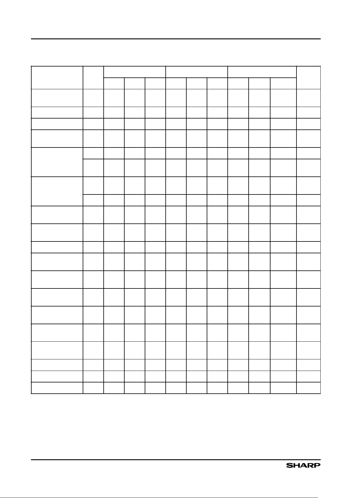
DC Characteristics
VCC = 3.3 V ± 0.3 V, TA = 0°C to +70°C
3/5» = Pin Set High for 3.3 V Operations
SYMBOL PARAMETER TYP. MIN. MAX. UNITS TEST CONDITI ONS NOTE
I
IL
Input Load Current ±1 µA VCC = VCC MAX., VIN = VCC or GND 1
I
LO
Output Leakage Current ±10 µA VCC = VCC MAX., VIN = VCC or GND 1
I
CCS
VCC Standby Current
48µA
V
CC
= VCC MAX.,
CE
»
0
, CE
»
1
, RP
»
= VCC ±0.2 V
BYTE, WP, 3/5
» = V
CC
±0.2 V or GND
±0.2 V
1,4
14mA
V
CC
= VCC MAX.,
CE
»
0
, CE
»
1
, RP
» = V
IH
BYTE, WP, 3/5
»
= VIH or V
IL
I
CCD
VCC Deep Power-Down
Current
15µA
RP
»
= GND ±0.2 V
1
I
CCR
1
VCC Read Current 30 35 mA
V
CC
= VCC MAX.,
CMOS: CE
»
0
, CE
»
1
= GND ±0.2 V
BYTE = GND ±0.2 V or VCC ±0.2 V
Inputs = GND ±0.2 V or VCC ±0.2 V
TTL: CE
»
0
, CE
»
1
= V
IL,
BYTE = VIH or V
IL
Inputs = V
IL
or V
IH
f = 8 MHz, I
OUT
= 0 mA
1, 3, 4
I
CCR
2
VCC Read Current 15 20 mA
VCC = VCC MAX.,
CMOS: CE
»
0
, CE
»
1
= GND ±0.2 V
BYTE = VCC ±0.2 V or GND ±0.2 V
Inputs = GND ±0.2 V or VCC ±0.2 V
TTL: CE
»
0
, CE
»
1
= V
IL,
BYTE = VIH or V
IL
Inputs = V
IL
or V
IH
f = 4 MHz, I
OUT
= 0 mA
1, 3, 4
I
CCW
VCC Write Current 8 12 mA Word/Byte Write in Progress 1
I
CCE
VCC Block Erase Current 6 12 mA Block Erase in Progress 1
I
CCES
VCC Erase Suspend
Current
36mA
CE
»
0
, CE
»
1
= V
IH
Block Erase Suspended
1, 2
I
PPS
VPP Standby Current ±1 ±10 µA VPP ≤ V
CC
1
I
PPD
VPP Deep Power-Down
Current
0.2 5 µA
RP
» = GND ±0.2 V
Page 19

16M (1M × 16, 2M × 8) Flash Memory LH28F016SU
19
DC Characteristics (Continued)
VCC = 3.3 V ± 0.3 V, TA = 0°C to +70°C
3/5» = Pin Set High for 3.3 V Operations
NOTES:
1. All currents are in RMS unless otherwise noted. Typical values at VCC = 3.3 V, VPP = 5.0 V, T = 25°C. These currents are valid for all
product versions (package and speeds).
2. I
CCES
is specified with the device de-selected. If the device is read while in erase suspend mode, current draw is the sum of
I
CCES
and I
CCR
.
3. Automatic Power Saving (APS) reduces I
CCR
to less than 1 mA in Static operation.
4. CMOS inputs are either VCC ± 0.2 V or GND ± 0.2 V. TTL Inputs are either VIL or VIH.
SYMBOL PARAMETER TYPE MIN. MAX. UNITS TEST CONDITIONS NOTE
I
PPR
VPP Read Current 200 µA VPP > V
CC
1
I
PPW
VPP Write Current 40 60 mA
VPP = V
PPH
, Word/Byte
Write in Progress
1
I
PPE
VPP Erase Current 20 40 mA
VPP = V
PPH
,
Block Erase in Progress
1
I
PPES
VPP Erase Suspend
Current
200 µA
VPP = V
PPH
,
Block Erase Suspended
1
V
IL
Input Low Voltage -0.3 0.8 V
V
IH
Input High Voltage 2.0 VCC + 0.3 V
V
OL
Output Low Voltage 0.4 V
VCC = VCC MIN. and
IOL = 4 mA
V
OH
1
Output High Voltage
2.4 V
IOH = 2.0 mA
VCC = VCC MIN.
V
OH
2
V
CC
- 0.2 V
IOH = 100 µA
VCC = VCC MIN.
V
PPL
VPP during Normal
Operations
0.0 5.5 V
V
PPH
VPP during Write/Erase
Operations
5.0 4.5 5.5 V
V
LKO
VCC Erase/Write
Lock Voltage
2.0 V
Page 20

LH28F016SU 16M (1M × 16, 2M × 8) Flash Memory
20
DC Characteristics
VCC = 5.0 V ± 0.5 V, TA = 0°C to +70°C
3.5» Pin Set Low for 5 V Operations
SYMBOL PARAMETER TYP. MIN. MAX. UNITS TEST CONDITIONS NOTE
I
IL
Input Load Current ±1 µA VCC = VCC MAX., VIN = VCC or GND 1
I
LO
Output Leakage Current ±10 µA VCC = VCC MAX., VIN = VCC or GND 1
I
CCS
VCC Standby Current
510µA
V
CC
= VCC MAX.,
CE
»
0
, CE
»
1
, RP
» = V
CC
±0.2 V
BYTE, WP, 3/5
»
= VCC ±0.2 V or
GND ±0.2 V
1,4
24mA
V
CC
= VCC MAX.,
CE
»
0
, CE
»
1
, RP
» = V
IH
BYTE, WP, 3/5
»
= VIH or V
IL
I
CCD
VCC Deep Power-Down
Current
15µA
RP
» = GND ±0.2 V
1
I
CCR
1
VCC Read Current 50 60 mA
V
CC
= VCC MAX.,
CMOS: CE
»
0
, CE
»
1
= GND ±0.2 V
BYTE = GND ±0.2 V or VCC ±0.2 V
Inputs = GND ±0.2 V or VCC ±0.2 V
TTL: CE
»
0
, CE
»
1
= V
IL,
BYTE = VIH or V
IL
Inputs = V
IL
or V
IH
f = 10 MHz, I
OUT
= 0 mA
1, 3, 4
I
CCR
2
VCC Read Current 30 35 mA
V
CC
= VCC MAX.,
CMOS: CE
»
0
, CE
»
1
= GND ±0.2 V
BYTE = VCC ±0.2 V or GND ±0.2 V
Inputs = GND ±0.2 V or VCC ±0.2 V
TTL: CE
»
0
, CE
»
1
= V
IL,
BYTE = VIH or V
IL
Inputs = V
IL
or V
IH
f = 5 MHz, I
OUT
= 0 mA
1, 3, 4
I
CCW
VCC Write Current 25 35 mA Word/Byte Write in Progress 1
I
CCE
VCC Block Erase Current 18 25 mA Block Erase in Progress 1
I
CCES
VCC Erase Suspend
Current
510mA
CE
»
0
, CE
»
1
= V
IH
Block Erase Suspended
1, 2
I
PPS
VPP Standby Current ±10 µA VPP ≤ V
CC
1
I
PPD
VPP Deep Power-Down
Current
0.2 5 µA
RP
»
= GND ±0.2 V
1
Page 21

16M (1M × 16, 2M × 8) Flash Memory LH28F016SU
21
DC Characteristics (Continued)
VCC = 5.0 V ± 0.5 V, TA = 0°C to +70°C
3.5» Pin Set Low for 5 V Operations
NOTES:
1. All currents are in RMS unless otherwise noted. Typical values at VCC = 5.0 V, VPP = 5.0 V, T = 25°C. These currents are valid for all
product versions (package and speeds).
2. I
CCES
is specified with the device de-selected. If the device is read while in erase suspend mode, current draw is the sum of
I
CCES
and I
CCR
.
3. Automatic Power Saving (APS) reduces I
CCR
to less than 2 mA in Static operation.
4. CMOS inputs are either VCC ± 0.2 V or GND ± 0.2 V. TTL Inputs are either VIL or VIH.
SYMBOL PARAMETER TYPE MI N. MAX. UNITS TEST CONDITIONS NOTE
I
PPR
VPP Read Current 65 200 µA VPP > V
CC
1
I
PPW
VPP Write Current 40 60 mA
VPP = V
PPH
, Word/Byte
Write in Progress
1
I
PPE
VPP Erase Current 20 40 mA
VPP = V
PPH
,
Block Erase in Progress
1
I
PPES
VPP Erase Suspend
Current
65 200 µA
VPP = V
PPH
,
Block Erase Suspended
1
V
IL
Input Low Voltage -0. 5 0.8 V
V
IH
Input High Voltage 2.0 VCC + 0.5 V
V
OL
Output Low Voltage 0.45 V
VCC = VCC MIN. and
IOL = 5.8 mA
V
OH
1
Output High Voltage
0.85 V
CC
V
IOH = -2.5 mA
VCC = VCC MIN.
V
OH
2
V
CC
- 0.4 V
IOH = -100 µA
VCC = VCC MIN.
V
PPL
VPP during Normal
Operations
0.0 5.5 V
V
PPH
VPP during Write/Erase
Operations
5.0 4.5 5.5 V
V
LKO
VCC Erase/Write
Lock Voltage
2.0 V
Page 22

LH28F016SU 16M (1M × 16, 2M × 8) Flash Memory
22
AC Characteristics - Read Only Operations
1
TA = 0°C to +70°C
SYMBOL PARAMETER
V
CC
= 3.3 V ± 0.3 V VCC = 2.7 V - 3.6 V
UNITS NOTE
MIN. MAX. MI N. MAX.
t
AVAV
Read Cycle Time 120 160 ns
t
AVEL
Address Setup to CE
» Going Low 10 10 ns 3, 4
t
AVGL
Address Setup to OE
» Going Low 0 0 ns 3, 4
t
AVQV
Address to Output Delay 120 160 ns
t
ELQV
CE
» to Output Delay 120 160 ns 2
t
PHQV
RP
»
High to Output Delay 620 650 ns
t
GLQV
OE
» to Output Delay 45 45 ns 2
t
ELQX
CE
» to Output in Low Z 0 0 ns 3
t
EHQZ
CE
» to Output in High Z 50 50 ns 3
t
GLQX
OE
» to Output in Low Z 0 0 ns 3
t
GHQZ
OE
» to Output in High Z 30 30 ns 3
t
OH
Output Hold from Address, CE
»
or
OE
»
change, whichever occurs first
00ns3
t
FLQV
t
FHQV
BYTE to Output Delay 120 160 ns 3
t
FLQZ
BYTE Low to Output in High Z 30 30 ns 3
t
ELFL
t
ELFH
BYTE High or Low to CE
» Low 5 5 ns 3
Page 23

16M (1M × 16, 2M × 8) Flash Memory LH28F016SU
23
AC Characteristics - Read Only Operations
1
Continued
TA = 0°C to +70°C
NOTES:
1. See AC Input/Output Reference Waveforms for timing measurements.
2. OE
»
may be delayed up to t
ELQV
- t
GLQV
after the falling edge of CE» without impact on t
ELQV
.
3. Sampled, not 100% tested.
4. This timing parameter is used to latch the correct BSR data onto the outputs.
SYMBOL PARAMETER
V
CC
= 5.0 V ± 0. 25 V VCC = 5.0 V ± 0.5 V
UNITS NOTE
MIN. MAX. MI N. MAX.
t
AVAV
Read Cycle Time
70 80
ns
t
AVEL
Address Setup to CE
» Going Low 10
10
ns 3, 4
t
AVGL
Address Setup to OE
» Going Low 0
0
ns 3, 4
t
AVQV
Address to Output Delay
70 80
ns
t
ELQV
CE
» to Output Delay 70
80
ns 2
t
PHQV
RP
»
High to Output Delay 400
480
ns
t
GLQV
OE
» to Output Delay 30
35
ns 2
t
ELQX
CE
» to Output in Low Z 0
0
ns 3
t
EHQZ
CE
» to Output in High Z 25
30
ns 3
t
GLQX
OE
» to Output in Low Z 0
0
ns 3
t
GHQZ
OE
» to Output in High Z 25
30
ns 3
t
OH
Output Hold from Address, CE
»
or
OE
»
change, whichever occurs first
0
0
ns 3
t
FLQV
t
FHQV
BYTE to Output Delay
70 80
ns 3
t
FLQZ
BYTE Low to Output in High Z
25 30
ns 3
t
ELFL
t
ELFH
CE
» Low to BYTE High or Low 5
5
ns 3
Page 24

LH28F016SU 16M (1M × 16, 2M × 8) Flash Memory
24
Figure 12. Read Timing Waveforms
28F016SUT-10
t
AVAV
NOTE: CEX is defined as the latter of CE0 or CE1 going LOW or the first of CE0 or CE1 going HIGH.
ADDRESSES STABLE
V
CC
POWER-UP
STANDBY
DEVICE AND
ADDRESS
SELECTION OUTPUTS ENABLED DATA VALID STANDBY
V
CC
POWER-DOWN
t
AVEL
ADDRESSES (A)
V
IH
V
IL
CEX (E)
(NOTE)
V
IH
V
IL
t
AVGL
t
GLQV
t
ELQV
t
GLQX
t
ELQX
t
AVQV
t
PHQV
t
EHQZ
t
GHQZ
t
OH
OE (G)
V
IH
V
IL
WE (W)
V
IH
V
IL
DATA (D/Q)
V
OH
V
OL
V
CC
5.0 V
GND
RP (P)
V
IH
V
IL
HIGH-Z HIGH-Z
VALID OUTPUT
. . .
. . .
. . .
. . .
. . .
. . .
. . .
Page 25

16M (1M × 16, 2M × 8) Flash Memory LH28F016SU
25
Figure 13. BY»TE» Timing W aveforms
28F016SUT-11
t
AVAV
NOTE: CEX is defined as the latter of CE0 or CE1 going LOW or the first of CE0 or CE1 going HIGH.
ADDRESSES STABLE
t
AVEL
= t
ELFL
ADDRESSES (A)
V
IH
V
IL
CEX (E)
(NOTE)
V
IH
V
IL
t
EHQZ
OE (G)
V
IH
V
IL
DATA (DQ0 - DQ7)
V
OH
V
OL
HIGH-Z HIGH-Z
BYTE (F)
V
IH
V
IL
V
OH
V
OL
HIGH-Z HIGH-Z
DATA
OUTPUT
DATA
OUTPUT
DATA
OUTPUT
t
AVEL
t
AVGL
t
ELFL
t
FLQV
= t
AVQV
t
GLQV
t
GHQZ
t
ELQV
t
ELQX
t
GLQX
t
OH
t
AVQV
t
FLQZ
DATA (DQ8 - DQ15)
. . .
. . .
. . .
. . .
. . .
. . .
. . .
Page 26

LH28F016SU 16M (1M × 16, 2M × 8) Flash Memory
26
Figure 14. VCC Power-Up and RP» Reset Waveforms
t
PLPH
t
AVQV
t
PHQV
t
PLPH
t
YHPH
t
YLPH
VALID
VALID
VALIDVALID
VALID
t
PLYL
t
PL5V
t
3VPH
3.0 V
0 V
3.3 V
4.5 V
5.0 V
t
5VPH
t
AVQV
t
AVQV
t
PHQV
t
PHQV
VALID
RP (P)
ADDRESS (A)
DATA (Q)
RP (P)
3/5 (Y)
V
CC
(3 V .5 V)
ADDRESS (A)
DATA (Q)
28F016SUT-12
Page 27

16M (1M × 16, 2M × 8) Flash Memory LH28F016SU
27
NOTES:
CE»0, CE»1 and OE
»
are switched low after Power-Up.
1. Minimum of 2 µs is required to meet the specified t
PHQV
times.
2. The power supply may start to switch concurrently with RP» going Low.
3. The address access time and RP» high to data valid time are shown for 5 V VCC operation.
Refer to the AC Characteristics Read Only Operations 3.3 V VCC operation and all other speed options.
SYMBOL PARAMETER MIN. MAX. UNIT NOTE
t
PLYL
t
PLYH
RP
» Low to 3/5 » Low (High) 0 µs
t
YLPH
t
YHPH
3/5
» Low (High) to RP » High 2 µs 1
t
PL5V
t
PL3V
RP
» Low to V
CC
at 4.5 V MIN.
(to VCC at 3.0 V min or 3.6 V MAX.)
0µs2
t
PLPH
RP
» 'Low' 100 ns
t
5VPH
VCC at 4.5 V to RP
» High 100 ns 3
t
3VPH
VCC at 3.0 V or RP
» High 100 ns 3
t
AVQV
Address Valid to Data Valid for VCC = 5 V ± 10% 100 ns 4
t
PHQV
RP
» High to Data Valid for V
CC
= 5 V ± 10% 480 ns 4
Page 28

LH28F016SU 16M (1M × 16, 2M × 8) Flash Memory
28
AC Characteristics for WE
»
- Controlled Command Write Operations
1
TA = 0°C to +70°C
SYMBOL PARAMETER TYP.
V
CC
= 3.3 ± 0.3 V
NOTE
MIN. MAX. UNITS
t
AVAV
Write Cycle Time 120 ns
t
VPWH
VPP Setup to WE Going High 100 ns 3
t
PHEL
RP
» Setup to CE » Going Low 480 ns
t
ELWL
CE
» Setup to WE Going Low 10 ns
t
AVWH
Address Setup to WE Going High 75 ns 2, 6
t
DVWH
Data Setup to WE Going High 75 ns 2, 6
t
WLWH
WE Pulse Wi dth 75 ns
t
WHDX
Data Hold from WE High 10 ns 2
t
WHAX
Address Hold from WE High 10 ns 2
t
WHEH
CE
»
Hold from WE High 10 ns
t
WHWL
WE Pulse Width High 75 ns
t
GHWL
Read Recovery before Write 0 ns
t
WHRL
WE High to RY
»/BY » Going Low 100 ns
t
RHPL
RP
»
Hold from Valid Status Register
(CSR, GSR, BSR) Data and RY
»
/BY
»
High
0ns3
t
PHWL
RP
» High Recovery to WE Going Low 1 µs
t
WHGL
Write Recovery before Read 120 ns
t
QVVL
VPP Hold from Valid Status Register
(CSR, GSR, BSR) Data and RY
»/BY » High
0µs
t
WHQV
1
Duration of Byte Write Operation 12 5 µs 4, 5
t
WHQV
2
Duration of Block Erase Operation 0.3 s 4
Page 29

16M (1M × 16, 2M × 8) Flash Memory LH28F016SU
29
AC Characteristics for WE
»
- Controlled Command Write Operations1 (Continued)
TA = 0°C to +70°C
NOTES:
CE» is defined as the latter of CE»0 or CE»1 going Low or the first of CE»0 or CE»1 going High.
1. Read timing during write and erase are the same as for normal read.
2. Refer to command definition tables for valid address and data values.
3. Sampled, but not 100% tested.
4. Write/Erase durations are measured to valid Status Register (CSR) Data.
5. Word/Byte write operations are typically performed with 1 Programming Pulse.
6. Address and Data are latched on the rising edge of WE
»
for all Command Write Operations.
SYMBOL PARAMETER
V
CC
= 5.0 ± 0.25 V VCC = 5.0 ± 0.5 V
UNITS NOTE
TYP. MIN. MAX. TYP. MIN. MAX.
t
AVAV
Write Cycle Time 70 80 ns
t
VPWH
VPP Setup to WE Going High 100 100 ns 3
t
PHEL
RP
» Setup to CE » Going Low 480 480 ns
t
ELWL
CE
» Setup to WE Going Low 0 0 ns
t
AVWH
Address Setup to WE Going High 50 50 ns 2, 6
t
DVWH
Data Setup to WE Going High 50 50 ns 2, 6
t
WLWH
WE Pulse Wi dth 40 50 ns
t
WHDX
Data Hold from WE High 0 10 ns 2
t
WHAX
Address Hold from WE High 10 10 ns 2
t
WHEH
CE
»
Hold from WE High 10 10 ns
t
WHWL
WE Pulse Width High 30 30 ns
t
GHWL
Read Recovery before Write 0 0 ns
t
WHRL
WE High to RY
»/BY » Going Low 100 100 ns
t
RHPL
RP
»
Hold from Valid Status Register
(CSR, GSR, BSR) Data and
RY
»
/BY
»
High
00ns3
t
PHWL
RP
» High Recovery to WE Going Low 1 1 µs
t
WHGL
Write Recovery before Read 60 65 ns
t
QVVL
VPP Hold from Valid Status Register
(CSR, GSR, BSR) Data and
RY
»/BY » High
00µs
t
WHQV
1
Duration of Word/Byte Write Operation 8 4.5 8 4.5 µs 4, 5
t
WHQV
2
Duration of Block Erase Operation 0.3 0.3 s 4
Page 30

LH28F016SU 16M (1M × 16, 2M × 8) Flash Memory
30
Figure 15. AC Waveforms for Command Write Operations
ADDRESSES (A)
(NOTE 1)
V
IH
V
IL
A
IN
A = RA
V
IH
V
IL
A
IN
A = RA
D
IN
D
IN
D
IN
D
IN
D
OUT
CEX (E)
(NOTE 4)
V
IH
V
IL
OE (G)
V
IH
V
IL
WE (W)
V
IH
V
IL
DATA (D/Q)
V
IH
V
IL
RY/BY (R)
V
OH
V
OL
RP (P)
V
IH
V
IL
t
AVAV
t
AVAV
t
WHGL
t
WHWL
t
WLWH
t
DVWH
t
PHWL
t
RHPL
t
QVVL
ADDRESSES (A)
(NOTE 2)
t
AVWH
t
WHAX
t
AVWHtWHAX
t
ELWL
t
WHEH
t
WHQV 1, 2
t
GHWL
t
WHDX
t
WHRL
(NOTE 5)
t
VPWH
28F016SUT-13
(NOTE 3)
HIGH-Z
WRITE
DATA-WRITE
OR ERASE
SETUP COMMAND
DEEP
POWER-DOWN
WRITE VALID
ADDRESS AND DATA
(DATA-WRITE) OR
ERASE CONFIRM
COMMAND
AUTOMATED
DATA-WRITE
OR ERASE
DELAY
WRITE READ
EXTENDED
REGISTER
COMMAND
READ
EXTENDED
STATUS
REGISTER DATA
NOTES:
1. This address string depicts Data-Write/Erase cycles with corresponding verification via ESRD.
2. This address string depicts Data-Write/Erase cycles with corresponding verification via CSRD.
3. This cycle is invalid when using CSRD for verification during Data-Write/Erase operations.
4. CEX is defined as the latter of CE0 or CE1 going LOW or the first of CE0 or CE1 going HIGH.
5. RP low transition is only to show t
RHPL
; not valid for above Read and Write cycles.
READ
COMPATIBLE
STATUS
REGISTER DATA
V
PP
(V)
V
PPH
V
PPL
Page 31

16M (1M × 16, 2M × 8) Flash Memory LH28F016SU
31
AC Characteristics for CE» - Controlled Command Write Operations
1
TA = 0°C to +70°C
SYMBOL PARAMETER
V
CC
= 3.3 V ± 0.3 V
UNITS NOTE
TYP. MIN. MAX.
t
AVAV
Write Cycle Time 150 ns
t
PHWL
RP
»
Setup to WE Going Low 480 ns 3
t
VPEH
VPP Set up to CE
» Going High 100 ns 3
t
WLEL
WE Setup to CE
» Going Low 0 ns
t
AVEH
Address Setup to CE
»
Going High 75 ns 2, 6
t
DVEH
Data Setup to CE
» Going High 75 ns 2, 6
t
ELEH
CE
» Pulse Width 75 ns
t
EHDX
Data Hold from CE
» High 10 ns 2
t
EHAX
Address Hold from CE
» High 10 ns 2
t
EHWH
WE Hold f rom CE
»
High 10 ns
t
EHEL
CE
» Pulse Width High 75 ns
t
GHEL
Read Recovery before Write 0 ns
t
EHRL
CE
» High to RY »/BY » Going Low 100 ns
t
RHPL
RP
»
Hold from Valid Status Register
(CSR, GSR, BSR) Data and RY
»
/BY
»
High
0ns3
t
PHEL
RP
» High Recovery t o CE » Going Low 1 µs
t
EHGL
Write Recovery before Read 120 ns
t
QVVL
VPP Hold from Valid Status Register
(CSR, GSR, BSR) Data and RY
»/BY » High
0µs
t
EHQV
1
Duration of Byte Write Operation 12 5 µs 4, 5
t
EHQV
2
Duration of Block Erase Operation 0.3 s 4
Page 32

LH28F016SU 16M (1M × 16, 2M × 8) Flash Memory
32
NOTES:
CE» is defined as the latter of CE»0 or CE»1 going Low or the first of CE»0 or CE»1 going High.
1. Read timing during write and erase are the same as for normal read.
2. Refer to command definition tables for valid address and data values.
3. Sampled, but not 100% tested.
4. Write/Erase durations are measured to valid Status Register (CSR) Data.
5. Word/Byte write operations are typically performed with 1 Programming Pulse.
6. Address and Data are latched on the rising edge of CE» for all Command Write Operations.
AC Characteristics for CE» - Controlled Command Write Operations1 (Continued)
TA = 0°C to +70°C
SYMBOL PARAMETER
V
CC
= 5.0 V ± 0.25 V VCC = 5.0 V ± 0.5 V
UNITS NOTE
TYP. MIN. MAX. TYP. MIN. MAX.
t
AVAV
Write Cycle Time 70 80 ns
t
PHWL
RP
»
Setup to WE Going Low 480 480 ns 3
t
VPEH
VPP Set up to CE
» Going High 100 100 ns 3
t
WLEL
WE Setup to CE
» Going Low 0 0 ns
t
AVEH
Address Setup to CE
»
Going High 50 50 ns 2, 6
t
DVEH
Data Setup to CE
» Going High 50 50 ns 2, 6
t
ELEH
CE
» Pulse Width 40 50 ns
t
EHDX
Data Hold from CE
» High 0 0 ns 2
t
EHAX
Address Hold from CE
» High 10 10 ns 2
t
EHWH
WE Hold f rom CE
»
High 10 10 ns
t
EHEL
CE
» Pulse Width High 30 50 ns
t
GHEL
Read Recovery before Write 0 0 ns
t
EHRL
CE
» High to RY »/BY » Going Low 100 100 ns
t
RHPL
RP
»
Hold from Valid Status Register
(CSR, GSR, BSR) Data and
RY
»
/BY
»
High
00ns3
t
PHEL
RP
» High Recovery t o CE » Going Low 1 1 µs
t
EHGL
Write Recovery before Read 60 80 ns
t
QVVL
VPP Hold from Valid Status Register
(CSR, GSR, BSR) Data and
RY
»/BY » High
00µs
t
EHQV
1
Duration of Byte Write Operation 8 4.5 8 4.5 µs 4, 5
t
EHQV
2
Duration of Block Erase Operation 0.3 0.3 s 4
Page 33

16M (1M × 16, 2M × 8) Flash Memory LH28F016SU
33
Figure 16. Alternate AC Waveforms for Command Write Operations
ADDRESSES (A)
(NOTE 1)
V
IH
V
IL
A
IN
A = RA
V
IH
V
IL
A
IN
D
IN
D
IN
D
IN
D
IN
D
OUT
CEX (E)
(NOTE 4)
V
IH
V
IL
OE (G)
V
IH
V
IL
WE (W)
V
IH
V
IL
DATA (D/Q)
V
IH
V
IL
RY/BY (R)
V
OH
V
OL
RP (P)
V
IH
V
IL
t
AVAV
t
AVAV
t
EHGL
t
EHEL
t
ELEH
t
DVEH
t
PHEL
t
RHPL
t
QVVL
ADDRESSES (A)
(NOTE 2)
t
AVEH
t
EHAX
t
AVEHtEHAX
t
WLEL
t
EHWH
t
EHQV 1, 2
t
GHEL
t
EHDX
t
EHRL
(NOTE 5)
t
VPEH
28F016SUT-14
(NOTE 3)
HIGH-Z
WRITE
DATA-WRITE
OR ERASE
SETUP COMMAND
DEEP
POWER-DOWN
WRITE VALID
ADDRESS AND DATA
(DATA-WRITE) OR
ERASE CONFIRM
COMMAND
AUTOMATED
DATA-WRITE
OR ERASE
DELAY
WRITE READ
EXTENDED
REGISTER
COMMAND
NOTES:
1. This address string depicts Data-Write/Erase cycles with corresponding verification via ESRD.
2. This address string depicts Data-Write/Erase cycles with corresponding verification via CSRD.
3. This cycle is invalid when using CSRD for verification during Data-Write/Erase operations.
4. CE
X
is defined as the latter of CE0 or CE1 going LOW or the first of CE0 or CE1 going HIGH.
5. RP low transition is only to show t
RHPL
; not valid for above Read and Write cycles.
V
PP
(V)
V
PPH
V
PPL
READ
EXTENDED
STATUS
REGISTER DATA
READ
COMPATIBLE
STATUS
REGISTER DATA
Page 34

LH28F016SU 16M (1M × 16, 2M × 8) Flash Memory
34
AC Characteristics for Page Buffer Write Operations
1
TA = 0°C to +70°C
NOTES:
CE» is defined as the latter of CE»0 or CE»1 going Low or the first of CE»0 or CE»1 going High.
1. These are WE
»
controlled write timings, equivalent CE» controlled write timings apply.
2. Sampled, but not 100% tested.
3. Address must be valid during the entire WE
»
Low pulse.
SYMBOL PARAMETER
V
CC
= 3.3 V ± 0.3 V
UNITS NOTE
TYP. MIN. MAX.
t
AVAV
Write Cycle Time 120 ns
t
ELWL
CE
» Setup to WE Going Low 10 ns
t
AVWL
Address Setup to WE Going Low 0 ns 3
t
DVWH
Data Setup to WE Going High 75 ns 2
t
WLWH
WE Pulse Wi dth 75 ns
t
WHDX
Data Hold from WE High 10 ns 2
t
WHAX
Address Hold from WE High 10 ns 2
t
WHEH
CE
» Hold from WE High 10 ns
t
WHWL
WE Pulse Width High 45 ns
t
GHWL
Read Recovery before Write 0 ns
t
WHGL
Write Recovery before Read 95 ns
SYMBOL PARAMETER
V
CC
= 5.0 V ± 0.25 V VCC = 5.0 V ± 0.5 V
UNITS NOTE
TYP. MIN. MAX. TYP. MIN. MAX.
t
AVAV
Write Cycle Time 70 80 ns
t
ELWL
CE
» Setup to WE Going Low 0 0 ns
t
AVWL
Address Setup to WE Going Low 0 0 ns 3
t
DVWH
Data Setup to WE Going High 50 50 ns 2
t
WLWH
WE Pulse Wi dth 40 50 ns
t
WHDX
Data Hold from WE High 0 0 ns 2
t
WHAX
Address Hold from WE High 10 10 ns 2
t
WHEH
CE
» Hold from WE High 10 10 ns
t
WHWL
WE Pulse Width High 30 30 ns
t
GHWL
Read Recovery before Write 0 0 ns
t
WHGL
Write Recovery before Read 60 65 ns
Page 35

16M (1M × 16, 2M × 8) Flash Memory LH28F016SU
35
Figuer 17. Page Buffer Write Timing Waveforms
Erase and Word/Byte Write Performance
VCC = 3.3 V ± 0.3 V, TA = 0°C to +70°C
SYMBOL PARAMETER TYP.
(1)
MIN. MAX. UNITS TEST CONDITIONS NOTE
t
WHRH
1
Word/By te Wri te Ti me 12 µs 2
t
WHRH
2
Block Write Time 0.8 2.1 s Byte Write Mode
2
t
WHRH
3
Block Write Time 0.4 1.0 s Word Write Mode
2
Block Erase Time 0.9 10 s
2
Full Chip Erase Time 28.8 s
2
NOTES:
1. 25°C, VPP = 5.0 V.
2. Excludes System-Level Overhead.
VCC = 5.0 V ± 0.5 V, TA = 0°C to +70°C
SYMBOL PARAMETER TYP.
(1)
MIN. MAX. UNITS TEST CONDITIONS NOTE
t
WHRH
1
Byte Wri te Ti me
8
µs 2
t
WHRH
2
Block Wri te Tim e
0.54
2.1 s Byte Wri te Mo de
2
t
WHRH
3
Block Wri te Tim e
0.27
1.0 s Word Wri te Mo de
2
Block Erase Time
0.7
10 s
2
Full Chip Erase Time
22.4
s
2
VALID
ADDRESSES (A)
HIGH-Z
D
IN
t
DVWH
DATA (D/Q)
CEX (E)
WE (W)
t
WHDX
t
AVWL
t
WLWH
t
WHWL
t
WHEH
t
ELWL
t
WHAX
28F016SUT-15
Page 36

LH28F016SU 16M (1M × 16, 2M × 8) Flash Memory
36
ORDERING INFORMATION
56
0.50 [0.020] TYP.
29
28
1
PACKAGE BASE PLANE
0.28 [0.011]
0.12 [0.005]
20.30 [0.799]
19.70 [0.776]
18.60 [0.732]
18.20 [0.717]
19.30 [0.760]
18.70 [0.736]
0.49 [0.019]
0.39 [0.015]
0.22 [0.009]
0.02 [0.001]
1.10 [0.043]
0.90 [0.035]
1.19 [0.047] MAX.
0.13 [0.005]
0.18 [0.007]
0.08 [0.003]
14.20 [0.559]
13.80 [0.543]
56TSOP
56TSOP (TSOP056-P-1420)
DIMENSIONS IN MM [INCHES]
MAXIMUM LIMIT
MINIMUM LIMIT
LH28F016SU
Device TypeTPackage
28F016SUT-16
-##
Speed
70 70 ns
10 100 ns
56-pin, 1.2 mm x 14 mm x 20 mm TSOP (Type I) (TSOP056-P-1420)
Example: LH28F016SUT-70 (16M (1M x 16, 2M x 8) Flash Memory, 70 ns, 56-pin TSOP)
16M (1M x 16, 2M x 8) Flash Memory
Access Time (ns)
Page 37

SHARP reserves the right to make changes in specifications at any time and without notice. SHARP does not assume any responsibility
for the use of any circuitry described; no circuit patent licenses are implied.
NORTH AMERICA
EUROPE
ASIA
SHARP Electronics Corporation
Microelectronics Group
5700 NW Pacific Rim Blvd., M/S 20
Camas, WA 98607, U.S.A.
Phone: (360) 834-2500
Telex: 49608472 (SHARPCAM)
Facsimile: (360) 834-8903
http://www.sharpmeg.com
SHARP Electronics (Europe) GmbH
Microelectronics Division
Sonninstraße 3
20097 Hamburg, Germany
Phone: (49) 40 2376-2286
Telex: 2161867 (HEEG D)
Facsimile: (49) 40 2376-2232
LIFE SUPPORT POLICY
SHARP components should not be used in medical devices with life support functions or in safety equipment (or similiar applications
where component failure would result in loss of life or physical harm) without the written approval of an officer of the SHARP Corporation.
SHARP Corporation
Integrated Circuits Group
2613-1 Ichinomoto-Cho
Tenri-City, Nara, 632, Japan
Phone: (07436) 5-1321
Telex: LABOMETA-B J63428
Facsimile: (07436) 5-1532
WARRANTY
SHARP
warrants to Customer that the Products will be free from defects in material and workmanship under normal use and service for
a period of one year from the date of invoice. Customer's exclusive remedy for breach of this warranty is that SHARP will either (i) repair
or replace, at its option, any Product which fails during the warranty period because of such defect (if Customer promptly reported the
failure to
SHARP in writing) or, (ii) if SHARP is unable to repair or replace, SHARP will refund the purchase price of the Product upon its
return to SHARP. This warranty does not apply to any Product which has been subjected to misuse, abnormal service or handling, or
which has been altered or modified in design or construction, or which has been serviced or repaired by anyone other than SHARP. The
warranties set forth herein are in lieu of, and exclusive of, all other warranties, express or implied.
ALL EXPRESS AND IMPLIED
WARRANTIES OF
MERCHANTABILITY, FITNESS FOR USE AND FITNESS FOR A PARTICULAR PURPOSE ARE SPECIFICALLY
EXCLUDED.
®
©1997 by SHARP Corporation Reference Code SMT96111
Issued May 1996
16M (1M × 16, 2M × 8) Flash Memory LH28F016SU
 Loading...