

Page 1

In the absence of confirmation by device specification sheets, SHARP takes no responsibility for any defects that may occur in equipment using any SHARP devices shown in
catalogs, data books, etc. Contact SHARP in order to obtain the latest device specification sheets before using any SHARP device.
1
DESCRIPTION
The LH1694 is a 256-output TFT-LCD gate driver
IC.
FEATURES
• Number of LCD drive outputs : 256
• LCD drive output sequence :
Output shift direction can be selected
OG
1/OG256 or OG256/OG1
• Enable chain connection
• Usable with both positive/negative power supplies
• Output signal masking function
• Input signal voltage : +2.7 to +3.6 V
• LCD drive voltage : +16.0 to +42.0 V
• Operating temperature : –30 to +85 ˚C
• Package : 277-pin TCP (Tape Carrier Package)
PIN CONNECTIONS
LH1694
LH1694
256-output TFT-LCD Gate Driver IC
OG254
OG255
OG256
254
255
256
OG
1
OG2
OG3
1
2
3
CHIP SURFACE
VDD
VEE
VSS
VCC
VLS
GND
SVIO
R/L
CKV
OE1
OE2
OE3
SVOI
GND
TEST2
TEST1
VLS
VCC
VSS
VEE
VDD
277
276
275
274
273
272
271
270
269
268
267
266
265
264
263
262
261
260
259
258
257
277-PIN TCP
TOP VIEW
NOTE :
Doesn't prescribe TCP outline.
Page 2
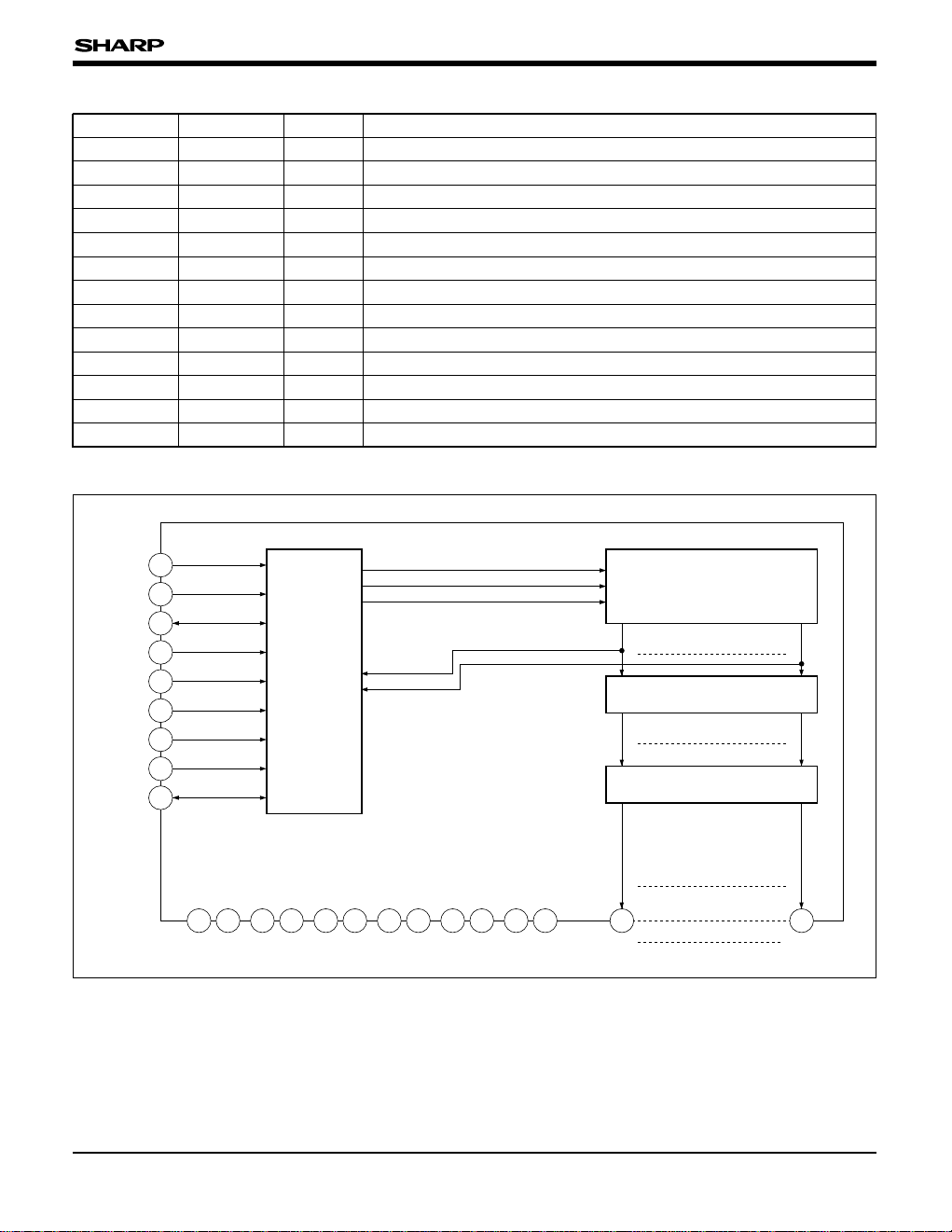
2
LH1694
PIN DESCRIPTION
BLOCK DIAGRAM
PIN NO. SYMBOL I/O DESCRIPTION
1 to 256 OG
1-OG256 O LCD drive output pins
257, 277 V
DD – Power supply pins for LCD drive
258, 276 VEE – Power supply pins for LCD drive
259, 275 V
SS – Power supply pins for logic system
260, 274 VCC – Power supply pins for logic system
261, 273 V
LS – Power supply pins for logic input/output systems
265 SVOI I/O Vertical scanning start pulse input/output pin
266 to 268 OE
3-OE1 I Input pins for output enable
269 CKV I Vertical shift clock input pin
270 R/L I Pin for selecting bi-directional shift register and setting cascade sequence
257
V
DD
262
263
TEST
1
TEST2
SVOI
OE
3
OE2
OE1
CKV
R/L
SVIO
265
266
267
268
269
270
271
V
DD
277 261
V
LS VLS
273 264
GND GND
272 260
V
CC VCC
274 258
V
EE VEE
276 259
V
SS VSS
275
OG
1
1
OG
256
256
OUTPUT CIRCUIT
LEVEL SHIFTER
BI-DIRECTIONAL SHIFT
REGISTER
CONTROL
LOGIC
1 256
1 256
1 256
IC test pinsITEST1, TEST2262, 263
Ground pins for logic input–GND264, 272
Vertical scanning start pulse input/output pinI/OSVIO271
Page 3
3
LH1694
FUNCTIONAL OPERATIONS OF EACH BLOCK
BLOCK FUNCTION
Control Logic
Used to create signals necessary for mode selecting signal, cascade sequence setting
signal and for operation of bi-directional shift register.
Bi-directional Shift
Register
Used as transfer circuit of LCD drive output start signal. It is possible to set LCD drive
output sequence of OG
1/OG256 direction or OG256/OG1 direction.
Level Shifter
Used as circuit which shifts LCD drive output signals transferred by bi-directional shift
register to V
DD-VEE level.
Output Circuit Configured with output buffers to output VDD-VEE level.
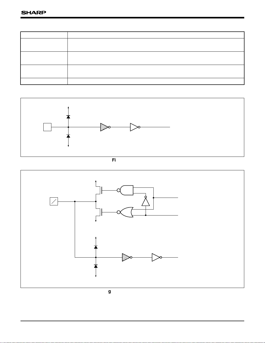
INPUT/OUTPUT CIRCUITS
I
V
LS
Level Shifter
(V
LS-GND/VCC-VSS)
Internal Logic
(VCC-VSS)
V
SS
To Internal Circuit
Fig. 1 Input Circuit
¿Applicable pins¡
CKV, R/L, OE
1-OE3,
TEST
1, TEST2
VLS
VSS
(VLS-GND)
Output Signal
Output Control Signal
VLS
Level Shifter
(V
LS-GND/VCC-VSS)
V
SS
To Internal Circuit
I
O
Fig. 2 Input/Output Circuit
¿Applicable pins¡
SVIO, SVOI
Page 4

4
LH1694
O
V
DD
(VDD-VEE)
VEE
From Internal Circuit
Fig. 3 Output Circuit
¿Applicable pins¡
OG
1-OG256
FUNCTIONAL DESCRIPTION
Pin Functions
SYMBOL FUNCTION
V
DD Used as power supply pin for high level LCD drive.
VLS Used as power supply pin for input level shifters.
V
CC Used as power supply pin for logic system, normally connected to VSS + 5.0 V.
VEE Used as power supply pin for low level LCD drive.
V
SS Used as logic system power supply pin.
CKV Used as vertical shift clock pulse input pin.
SVIO
SVOI
Used as vertical scanning start pulse input/output pins.
Data input/output pins for shift register. During input, data is read at the rising edge of the
CKV. During output, data is output at the falling edge of the CKV.
• When R/L = "H".
SVOI is set to data output pin for next cascade, and SVIO is set to input pin for shift data.
• When R/L = "L".
SVOI is set to input pin for shift data, and SVIO is set to data output pin for next cascade.
R/L
Used as input pin for selecting the shift direction of bi-directional shift register and for
setting the sequence of cascade connection.
LCD drive outputs shift from OG
1 to OG256 when set to "H". LCD drive outputs shift from
OG
256 to OG1 when set to "L".
OE
1
OE2
OE3
Input pins for output-enable. LCD drive output is set to "L", when OE1, OE2, and OE3 pins
are set to "H", and it has no relation with clock input.
Relationship between enable control and output pins;
OE
1 : OG1, OG4 π OG250, OG253, OG256
OE2 : OG2, OG5 π OG251, OG254
OE3 : OG3, OG6 π OG252, OG255
TEST1
TEST2
Used as input pins for IC testing.
Must be set to "H".
OG
1-OG256
Used as output pins for LCD drive output, and which output data at 2 levels.
• Selecting data is output at V
DD level .
• Non-selecting data is output at VEE level .
Used as power supply pin for input level shifters.GND
Page 5

5
LH1694
Example of Input/Output Timing (R/L = "H")
1234567 255256257258
CKV
SVIO
(Input)
OE
1
OE2
OE3
OG1
OG2
OG3
OG4
OG5
OG6
OG256
SVIO
(Output)
•
•
•
•
•
Functional Operations
LH1694 can select the LCD drive output level (OG1
to OG256) by the set of the input signal (CKV,
SVIO, SVOI, OE
1, OE2, OE3).
When the pin for selecting the bi-directional shift
register (R/L) is set to "H", LCD drive outputs shift
from OG
1 to OG256, and when set to "L", LCD
drive outputs shift from OG
256 to OG1.
OE
1,OE2 and OE3 are signals for output-enable.
Output pins output non-selecting data (V
EE level)
when OE
1 to OE3 pins are set to "H" and it has no
relation with input clock.
While R/L = "H" input data from SVIO is read at the
rising edge of shift clock (CKV), and outputs to
LCD drive output pin OG
1 at the width for one
cycle of shift clock. Next LCD drive output pins from
OG
2 to OG256 are sequentially shifted at the rising
edge of the CKV for one cycle. Shift signal of
OG
256 is read at the falling edge of the clock
signal, and the input data for the next cascade is
output from the SVOI pin.
While R/L = "L" input data from SVOI is read at the
rising edge of shift clock (CKV), and outputs to LCD
drive output pin OG
256 at the width for one cycle of
shift clock. Next LCD drive output pins from OG
255 to
OG
1 are sequentially shifted at the rising edge of the
CKV for one cycle. Shift signal of OG
1 is read at the
falling edge of the clock signal and the input data for
the next cascade is output from the SVIO pin.
Page 6

6
LH1694
PRECAUTIONS
Precautions when connecting or disconnecting
the power supply
This IC has a high-voltage LCD driver, so it may be
permanently damaged by a high current which may
flow if voltage is supplied to the LCD drive power
supply while the logic system power supply is
floating. Therefore, when connecting the power
supply, observe the following sequence.
Logic system power supply (V
LS) or internal
logic system power supply (V
SS, VCC; VCC >
V
SS) / logic input / LCD drive power supply
(V
EE, VDD)
It is possible to set voltage V
EE to the same as
V
SS. When connecting the power supply when VEE
= VSS, observe the following sequence and the
recommended sequence figure shown below.
Logic system power supply (V
LS), internal logic
system power supply (V
SS, VCC; VCC > VSS)
and low-level LCD drive power supply (V
EE) /
logic input / high-level LCD drive power supply
(V
DD)
When disconnecting the power supply, follow the
reverse sequence.
Since the logic state of the internal circuit is
unstable immediately after the logic system power
is supplied, input CKV and SVIO (or SVOI) while
initializing the internal circuit (minimum input clock
number is 256 CKV).
Input pin setting
Input pins other than CKV, SVIO and SVOI must
be set to "H" or "L" level.
Maximum ratings
When connecting or disconnecting the power, this
IC must be used within the range of the absolute
maximum ratings.
VDD
VLS
VCC
VSS, VEE
0 V
Input
Page 7

LH1694
7
ABSOLUTE MAXIMUM RATINGS
RECOMMENDED OPERATING CONDITIONS
PARAMETER SYMBOL APPLICABLE PINS RATING UNIT NOTE
Supply voltage
V
DD VDD –0.3 to +45.0 V
1, 2
V
LS VLS –0.3 to +7.0 V
VCC – VSS VCC, VSS –0.3 to +7.0 V
V
EE – VSS VEE, VSS –0.3 to +45.0 V
VDD – VEE
(VSS)
V
DD, VEE, VSS –0.3 to +45.0 V
Input voltage V
IN
CKV, SVIO, SVOI, R/L,
OE
1-OE3, TEST1, TEST2
–0.3 to VLS + 0.3 V
Storage temperature T
STG –45 to +125 ˚C
NOTES :
1. TA = +25 ˚C
2. The maximum applicable voltage on any pin with respect to 0 V.
NOTE :
1. The applicable voltage on any pin with respect to 0 V.
PARAMETER SYMBOL MAX. UNIT NOTE
Supply voltage
V
DD +35.0 V
1
Input voltage V
IN VLS V
Operating temperature T
OPR +85 ˚C
MIN. TYP.
+5.5
0
–30
V
LS
VCC
VEE – VSS
VDD – VEE
(VSS)
+2.7
VSS + 4.5
0
+16.0
+3.3
+25.0
+3.6 V
VSS + 5.5
V
+11.0 V
+42.0 V
V–5.0–20.0VSS
Each power supply pin of LH1694 is set as shown below.
Input SVIO/SVOI Output
V
DD
VLS
GND
V
CC
VSS, VEE
Internal Logic
LCD Drive Output
Page 8

8
LH1694
NOTES :
1. All input pins : 3.3 V
2. CKV : Frequency = 31 kHz, "L" period width t
WL = 16.2 µs
SVIO : Frequency = 60 Hz
OE
1 to OE3 : 0 V
Other input pins : 3.3 V
All output pins are opened.
PARAMETER
SYMBOL
CONDITIONS APPLICABLE PINS MIN. TYP. MAX. UNIT NOTE
Input "Low" voltage V
IL
VLS= 2.7 to 3.0 V
CKV, SVIO, SVOI,
OE1-OE3, R/L
0.2V
LS V
Input "High" voltage V
IH
VLS= 2.7 to 3.0 V
0.8VLS V
Output "Low" voltage V
OL IOL = 0.4 mA
VEE + 0.4
V
Output "High" voltage V
OH IOH = –0.4 mA
VDD – 0.4
V
Input "Low" current I
IL VI = 0 V 5.0 µA
Input "High" current IIH VI = VLS 5.0 µA
Supply current
I
DD 100 µA
2
ILS 1.5 mA
I
CC 100 µA
I
EE 100 µA
OG
1-OG256
CKV, SVIO, SVOI,
OE1-OE3, R/L 1
VLS= 3.0 to 3.6 V
0.3VLS V
VLS= 3.0 to 3.6 V
0.7VLS V
AC Characteristics (VLS = +2.7 to +3.6 V, VEE = VSS, TOPR = –30 to +85 ˚C)
PARAMETER
SYMBOL
CONDITIONS APPLICABLE PINS MIN. TYP. MAX. UNIT
Clock frequency f
CKV
CKV
100 kHz
"H" clock pulse width t
CLVH 1.0 µs
Clock rise time t
RCKV 100 ns
Clock fall time t
FCKV 100 ns
Data setup time tSU
CKV, SVIO, SVOI
100 ns
Data hold time t
H 300 ns
Pulse rise time t
RSPV 100 ns
Pulse fall time tFSPV 100 ns
Output transfer delay
time 1
t
DO
CL = 300 pF OG1-OG256
1.0 µs
Output rise time t
R 1.0 µs
Output fall time tF 1.0 µs
SVIO, SVOI
µs1.0t
CKVL"L" clock pulse width
µs1.0t
OEWOE enable time OE1-OE3
µs1.0tDSV
Output transfer delay
time 3
µs1.0t
DOE
Output transfer delay
time 2
C
L = 50 pF SVIO, SVOI
ELECTRICAL CHARACTERISTICS
DC Characteristics
(VLS = +2.7 to +3.6 V, VEE = VSS, TOPR = –30 to +85 ˚C)
Page 9

9
LH1694
CKV
SVIO
OG
1
OG2-OG256
CKV
OG256
SVIO
OE
1-OE3
OG1-OG256
50%
50%
90%
50%
50% 50%
10%
90%
50%
10%
50% 50%
50%
10%
10%
t
CKVH tCKVL fCKV
tFCKV
tRCKV
tSU
tRSPV
tFSPV
tDO tDO
tH
90%
t
DO tDO
50% 50%
50%
50% 50%
90%
10%
90%
10%
50%
t
R
tDSV
tOEW
tDOE tDOE
tDSV
tF
50%
50%
50%
50%
90%
VDD
VEE
VEE
VDD
VDD
VEE
VDD
VEE
Timing Chart
Page 10

PACKAGES FOR LCD DRIVERS
10
Tape width
ø Tape Specification ø Tape Material
48 mm
Tape type
Super wide
Perforation pitch
4 pitches
Substrate UPILEX S75
Adhesive E type
Cu foil [thickness]
VLP 25 µm
Solder resist Epoxy resin
Total
Backside
Pattern side
DUMMY
DUMMY
OG3
OG2
OG1
COM3
COM4
COM4
OG254
OG255
OG256
COM2
COM1
COM1
COM1
COM1
COM2
TEST2
VLS (TEST1)
VCC
VSS
VDD
VEE
GND
SVOI
OE3
OE2
OE1
CKV
R/L
SVIO
GND
VCC
VLS
VSS
VEE
VDD
COM3
COM4
COM4
2-Ø1.9 (PI)
Ø2.0
(Good device hole)
0.2
MAX.
1.1
MAX.
3.5 (SL)
3.4 (SR)
7.6 (SR)
2.0 (SL)
0.75
MAX.
13.85 (SR)
16.8 (SL) 0.9 (SL)0.9 (SL)
[3.5
TYP.
(3.2
MIN.
)]
1.42
±0.05
1.42
±0.05
4.75
±0.05
[0.5]
0.40
±0.02
0.40
±0.02
0.60
±0.02
0.60
±0.02
16.4 (SR)
0.40
±0.02
18.0
±0.7
16.8 (SL)
13.85 (SR)
4.2 (SR)
4.5 (SL)
5.0 (SL)
8.5 (SL)
7.0
±0.7
[7.0 (E.L.)]
[8.0]
[4.0 (E.L.)]
[6.9 (E.L.)]
5.4
±0.05
16.4 (SR)
Device center
Film center
Chip center
Sprocket center
(Resin area)
5.4
MAX.
2-R1.05 (SR)
20.4
MAX.
(Resin area)
32.6
±0.05
(Mark)
P0.12 x (264 – 1) = 31.56
±0.05
W0.060
±0.02
[34.0 (E.L.)]
[35.8]
29.8
±0.05
(Holes)
P1.00 x (26 – 1) = 25.0
±0.04
W0.40
±0.02
44.86
[30.0 (E.L.)]
28.0 (SL)
48.175
±0.2
1.5
±0.05
(Hole)
[13.9 (E.L.)]
2-Ø2.7 (Cu)
2-Ø1.5 (Cu hole)
LH1694F
PACKAGE (Unit : mm)
UPILEX is a trademark of UBE INDUSTRIES, LTD..
 Loading...