

Page 1
In the absence of confirmation by device specification sheets, SHARP takes no responsibility for any defects that may occur in equipment using any SHARP devices shown in
catalogs, data books, etc. Contact SHARP in order to obtain the latest device specification sheets before using any SHARP device.
1
DESCRIPTION
The LH1692 is a 300-output TFT-LCD gate driver
IC.
FEATURES
• Number of LCD drive outputs : 300
• LCD drive output sequence :
Output shift direction can be selected
OG
1/OG300 or OG300/OG1
• Cascade connection :
Max. 4 cascades (internal counting system)
• Usable with both positive/negative power supplies
• Output mode selection
– Normal mode (1-pulse scanning)
– Continuous 2-pulse mode (2-pulse scanning)
– Jumping 2-pulse mode (2-pulse scanning)
• LCD drive voltage : +16.0 to +42.0 V
• Operating temperature : –30 to + 85 ˚C
• Package : 319-pin TCP (Tape Carrier Package)
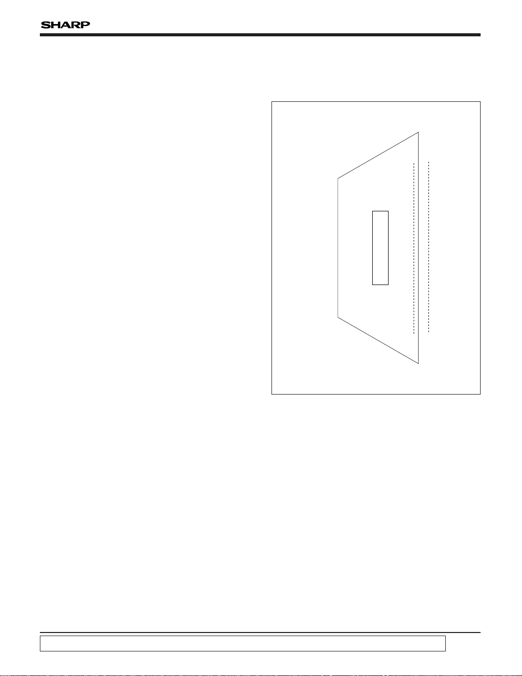
PIN CONNECTIONS
LH1692
LH1692
OG298
OG299
OG300
298
299
300
OG
1
OG2
OG3
1
2
3
CHIP SURFACE
VDD
VEE
VSS
VCC
VLS
TEST1
TEST2
CKV
SPV
CE1
CE2
R/L
MODE1
MODE2
V
LS
VCC
VSS
VEE
VDD
319
318
317
316
315
314
313
312
311
310
309
308
307
306
305
304
303
302
301
319-PIN TCP
TOP VIEW
NOTE :
Doesn't prescribe TCP outline.
300-output TFT-LCD Gate Driver IC
Page 2
LH1692
2
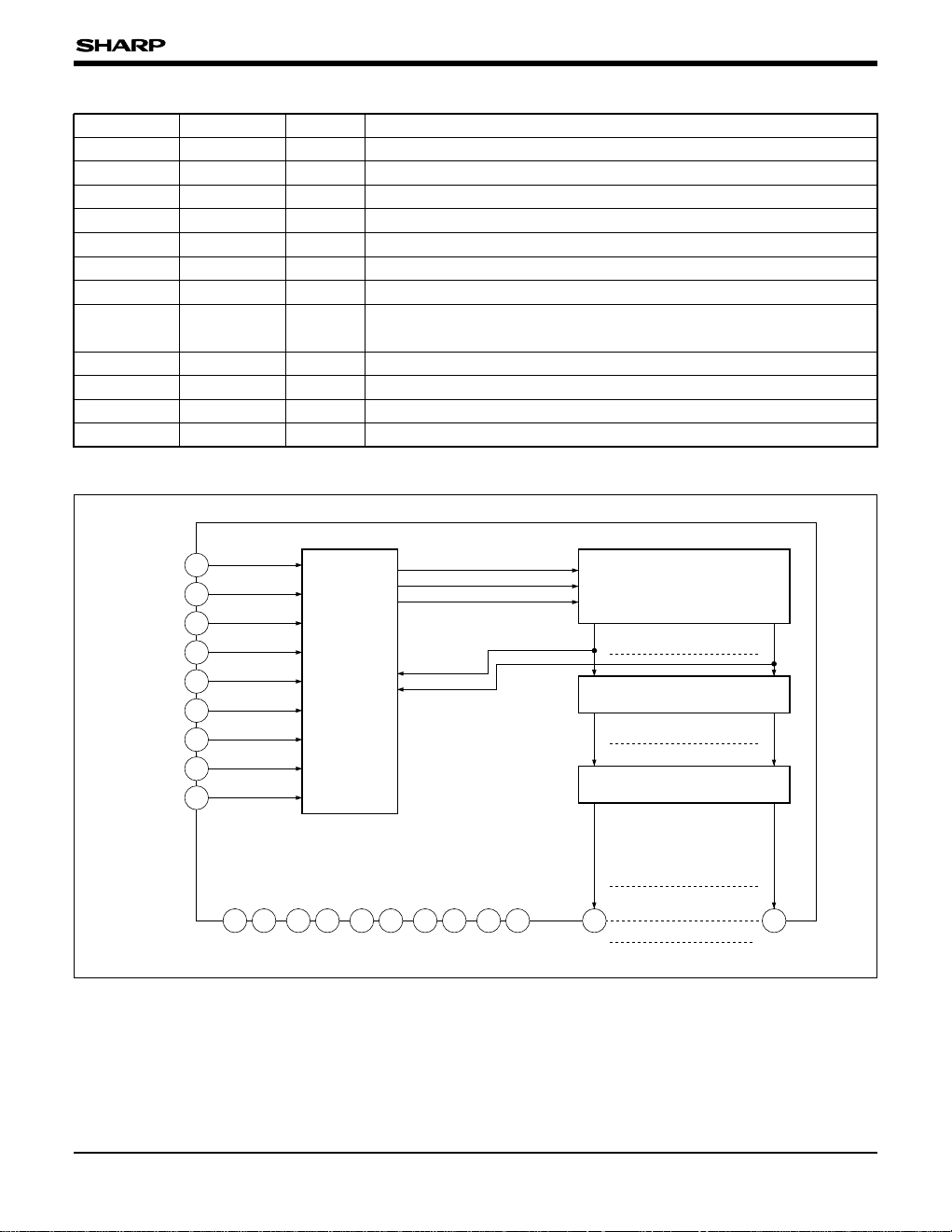
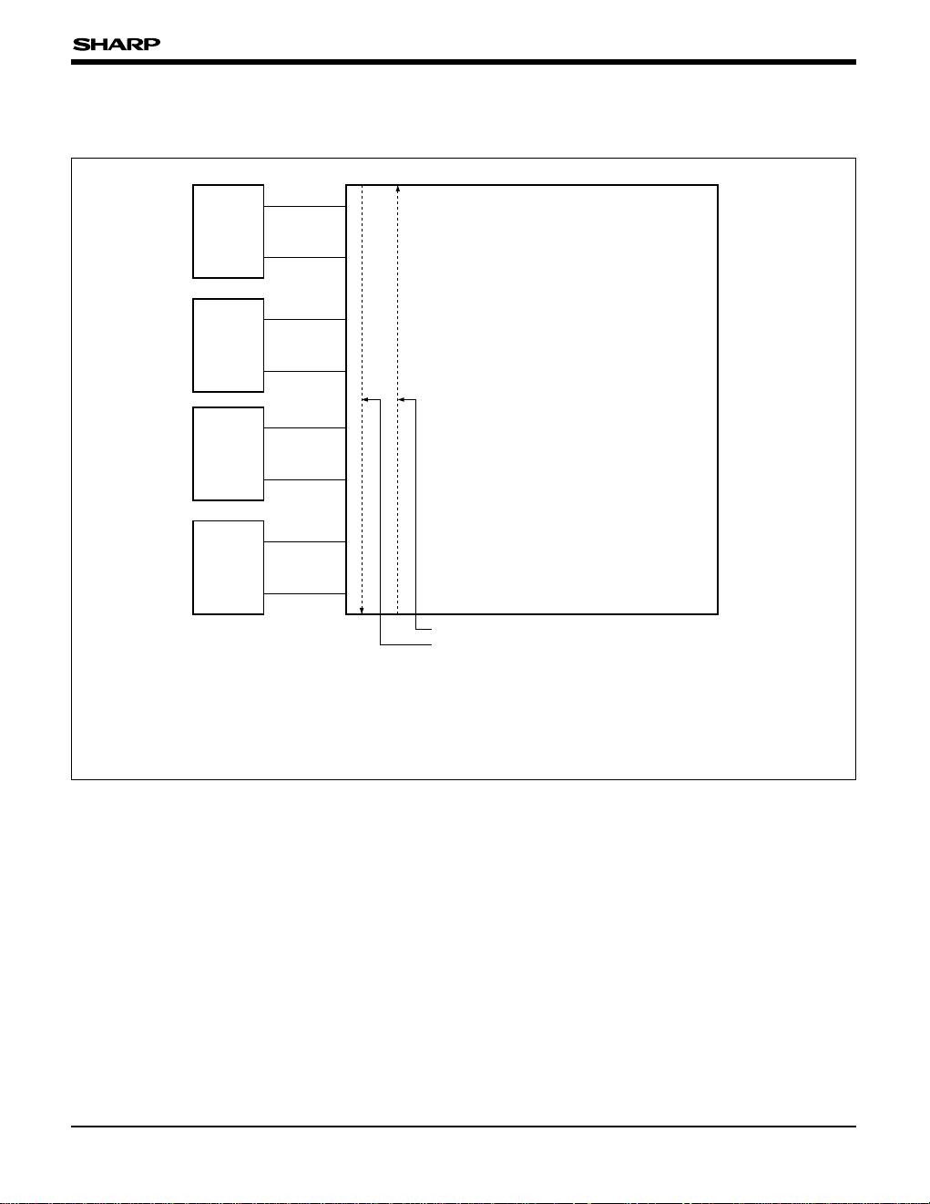
BLOCK DIAGRAM
PIN NO. SYMBOL I/O DESCRIPTION
1 to 300 OG
1-OG300 O LCD drive output pins
301, 309 V
DD – Power supply pins for LCD drive
302, 318 VEE – Power supply pins for LCD drive
303, 317 V
SS – Power supply pins for logic system
304, 316 VCC – Power supply pins for logic system
305, 315 V
LS – Power supply pins for input level shifter
309, 310 CE
2, CE1 I Cascade sequence setting pins
311 SPV I Vertical scanning start pulse input pin
312 CKV I Vertical shift clock input pin
313, 314 TEST
2, TEST1 I IC test pins
301
V
DD
306
307
MODE
2
MODE1
R/L
CE
2
CE1
SPV
CKV
TEST
2
TEST1
308
309
310
311
312
313
314
V
DD
319 305
V
LS VLS
315 304
V
CC VCC
316 302
V
EE VEE
318 303
V
SS VSS
317
OG
1
1
OG
300
300
OUTPUT CIRCUIT
LEVEL SHIFTER
BI-DIRECTIONAL SHIFT
REGISTER
CONTROL
LOGIC
1 300
1 300
1 300
Pin for selecting bi-directional shift register and setting cascade
sequence
IR/L308
Output mode selection pinsI
MODE2, MODE
1
306, 307
PIN DESCRIPTION
Page 3
LH1692
3
BLOCK FUNCTION
Control Logic
Used to create signals necessary for mode selecting signal, cascade sequence setting
signal and for operation of bi-directional shift register.
Bi-directional Shift
Register
Used as transfer circuit of LCD drive output start signal. It is possible to set LCD drive
output sequence of OG
1/OG300 direction or OG300/OG1 direction.
Level Shifter
Used as circuit which shifts LCD drive output signals transferred by bi-directional shift
register to V
DD-VEE level.
Output Circuit Configured with output buffers to output VDD-VEE level.
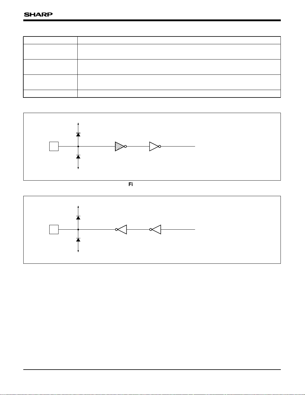
INPUT/OUTPUT CIRCUITS
I
V
LS
Level Shifter
(V
LS-0 V/VCC-VSS)
Internal Logic
(VCC-VSS)
V
SS
To Internal Circuit
Fig. 1 Input Circuit
¿Applicable pins¡
SPV, CKV, CE1, CE2,
R/L, MODE
1, MODE2,
TEST
1, TEST2
O
V
DD
(VDD-VEE)
VEE
From Internal Circuit
Fig. 2 Output Circuit
¿Applicable pins¡
OG
1-OG300
FUNCTIONAL OPERATIONS OF EACH BLOCK
Page 4
LH1692
4
SYMBOL FUNCTION
V
DD Used as power supply pin for high level LCD drive.
V
LS Used as power supply pin for input level shifters.
VCC Used as power supply pin for logic system, normally connected to VSS + 5.0 V.
V
EE Used as power supply pin for low level LCD drive.
VSS Used as logic system power supply pin.
CKV Used as vertical shift clock pulse input pin.
SPV
Used as vertical scanning start pulse input pin. (At least, input one cycle of CKV during "L"
period of SPV.)
MODE
1
MODE2
Used as input pins for selecting output mode.
Output mode is set as shown in the table below by setting MODE1 pin and MODE2 pin.
R/L
Used as input pin for selecting the shift direction of bi-directional shift register and for
setting the sequence of cascade connection.
LCD drive outputs shift from OG
1 to OG300 when set to "H". LCD drive outputs shift from
OG
300 to OG1 when set to "L". At the same time, cascade sequence is set as shown in
the table below.
CE
1
CE2
Used as input pins for setting of chip cascade sequence. (Max. 4 cascades)
With above setting, sets the cascade sequence signal inside the IC.
TEST
1
TEST2
Used as input pins for IC testing.
Must be set to "H".
OG
1-OG300
Used as output pins for LCD drive output, and which output data at 2 levels.
• Selecting data is output at VDD level .
• Non-selecting data is output at V
EE level .
MODE
1 MODE2 Output mode
H H Normal mode (1-pulse scanning)
L H Continuous 2-pulse mode
H L Jumping 2-pulse mode
L L Set all outputs to V
EE level.
CE
1
Cascade sequence
R/L = "H"
1st
2nd
R/L = "L"
4th
3rd
H
L
L 1st4th
H 2nd3rdL
L
H
H
CE
2
FUNCTIONAL DESCRIPTION
Pin Functions
Page 5
LH1692
5
TFT-LCD Panel
Scanning Direction When R/L = "L".
Scanning Direction When R/L = "H".
OG
1
OG300
OG1
OG300
OG1
CE1 = "H"
CE
2 = "H"
CE
1 = "L"
CE
2 = "H"
CE
1 = "H"
CE
2 = "L"
CE
1 = "L"
CE
2 = "L"
OG
300
OG1
OG300
At this time, normal mode (scanning with 1 pulse) is set when MODE1 = "H" and MODE2 = "H",
jumping 2-pulse mode (scanning with 2 pulses) is set when MODE
1 = "H" and MODE2 = "L",
continuous 2-pulse mode (scanning with 2 pulses) is set when MODE
1 = "L" and MODE2 = "H", and
output V
EE level is set when MODE1 = "L" and MODE2 = "L".
*
Functional Operations
(1) Example of Cascade Sequence (One Side Assembled)
Page 6

LH1692
6
(2) Example of Input/Output Timing (For 1st Cascade Sequence)
CKV
SPV
OG
300OG1
OG299OG2
OG298OG3
OG300OG1
OG299OG2
OG298OG3
R/L = "H" R/L = "L"
(1-pulse Mode)
(Jumping 2-pulse Mode)
Page 7

LH1692
7
TFT-LCD Panel
Scanning Direction When R/L = "L".
Scanning Direction When R/L = "H".
OG
1
OG300
OG1
CE1 = "H"
CE
2 = "H"
CE
1 = "L"
CE
2 = "H"
OG
300
OG300
OG1
CE1 = "H"
CE
2 = "L"
CE
1 = "L"
CE
2 = "L"
OG300
OG1
At this time, normal mode (scanning with 1 pulse) is set when MODE1 = "H" and MODE2 = "H",
jumping 2-pulse mode (scanning with 2 pulses) is set when MODE
1 = "H" and MODE2 = "L",
continuous 2-pulse mode (scanning with 2 pulses) is set when MODE
1 = "L" and MODE2 = "H", and
output V
EE level is set when MODE1 = "L" and MODE2 = "L".
*
(3) Example of Cascade Sequence (Both Side Assembled)
Page 8

LH1692
8
CKV
SPV
OG
300OG1
OG299OG2
OG298OG3
OG300OG1
OG299OG2
OG298OG3
R/L = "H" R/L = "L"
(1-pulse Mode)
(Continuous 2-pulse Mode)
(4) Example of Input/Output Timing (For 1st Cascade Sequence)
Page 9

LH1692
9
PRECAUTIONS
Precautions when connecting or disconnecting
the power supply
This IC has a high-voltage LCD driver, so it may be
permanently damaged by a high current which may
flow if voltage is supplied to the LCD drive power
supply while the logic system power supply is
floating. Therefore, when connecting the power
supply, observe the following sequence.
Logic system power supply (V
LS) or internal
logic system power supply (V
SS, VCC; VCC >
V
SS) / logic input / LCD drive power supply
(V
EE, VDD)
It is possible to set voltage V
EE to the same as
V
SS. When connecting the power supply when VEE
= VSS, observe the following sequence and the
recommended sequence figure shown below.
Logic system power supply (V
LS), internal logic
system power supply (V
SS, VCC; VCC > VSS)
and low-level LCD drive power supply (V
EE) /
logic input / high-level LCD drive power supply
(V
DD)
When disconnecting the power supply, follow the
reverse sequence.
Since the logic state of the internal circuit is
unstable immediately after the logic system power
is supplied, input CKV and SPV while initializing the
internal circuit (minimum input clock number is 300
CKV).
MODE
1 and MODE2 should be set to "L" during
the initializing period for setting the LCD drive
output to V
EE level.
Input pin setting
Input pins other than CKV and SPV must be set to
"H" or "L" level.
Maximum ratings
When connecting or disconnecting the power, this
IC must be used within the range of the absolute
maximum ratings.
VDD
VLS
VCC
VSS, VEE
0 V
Input
Page 10

LH1692
10
RECOMMENDED OPERATING CONDITIONS
PARAMETER SYMBOL APPLICABLE PINS RATING UNIT NOTE
Supply voltage
V
DD VDD –0.3 to +45.0 V
1, 2
V
LS VLS –0.3 to +7.0 V
VCC – VSS VCC, VSS –0.3 to +7.0 V
V
EE – VSS VEE, VSS –0.3 to +45.0 V
VDD – VEE
(VSS)
V
DD, VEE, VSS –0.3 to +45.0 V
Input voltage V
IN
CKV, SPV, CE1, CE2, R/L,
MODE1, MODE2, TEST
1
, TEST
2
–0.3 to VLS + 0.3 V
Storage temperature T
STG –45 to +125 ˚C
NOTES :
1. TA = +25 ˚C
2. The maximum applicable voltage on any pin with respect to 0 V.
NOTES :
1. The applicable voltage on any pin with respect to 0 V.
2. Ensure that voltages are set as follows.
V
SS, VEE ≤ 0 V
V
CC – VSS = VLS±0.1 V (For 3.3 V specifications)
V
CC – VSS = VLS±0.2 V (For 5.0 V specifications)
V
CC ≤ VLS
PARAMETER SYMBOL MAX. UNIT NOTE
Supply voltage
V
DD +42.0 V
1, 2
Input voltage V
IN VLS V
Operating temperature T
OPR +85 ˚C
MIN. TYP.
+5.5 +9.0
0
–30
V
LS
VCC – VSS
VEE – VSS
VDD – VEE
(VSS)
+3.0
+3.0
0
+16.0
+5.0
+5.0
+25.0
+5.5 V
+5.5 V
+11.0 V
+42.0 V
ABSOLUTE MAXIMUM RATINGS
Page 11

LH1692
11
Input
V
LS, VCC
VDD
VSS, VEE (0 V)
Internal Logic
LCD Drive Output
Example 2 : For Negative Voltage Output
When power supply pins are set as shown below,
the LH1692 can output positive voltage and
negative voltage to LCD drive output.
Example 1 : For Positive Voltage Output
VDD, VLS
0 V
V
CC
VSS, VEE
Input
LCD Drive Output
Internal Logic
Page 12

LH1692
12
NOTES :
1. All input pins : 3.3 V
2. CKV : Frequency = 31 kHz, "L" period width t
WL = 16.2 µs
SPV : Frequency = 60 Hz
Other input pins : 3.3 V
All output pins are opened.
3. CKV : Frequency = 31 kHz, "L" period width t
WL = 16.2 µs
SPV : Frequency = 60 Hz
MODE
2 : 0 V
Other input pins : 3.3 V
All output pins are opened.
4. CKV : Frequency = 31 kHz, "L" period width t
WL = 16.2 µs
SPV : Frequency = 60 Hz
MODE
1 : 0 V
Other input pins : 3.3 V
All output pins are opened.
PARAMETER
SYMBOL
CONDITIONS APPLICABLE PINS MIN. TYP. MAX. UNIT NOTE
Input "Low" voltage V
IL CKV, SPV, MODE1,
MODE
2, CE1, CE2, R/L
0.2V
LS V
Input "High" voltage V
IH 0.8VLS V
Output "Low" voltage VOL IOL = 0.4 mA
VEE + 0.4
V
Output "High" voltage V
OH IOH = –0.4 mA
VDD – 0.4
V
Input "Low" current I
IL VI = 0 V 5.0 µA
Input "High" current IIH VI = VLS 5.0 µA
Supply current (1)
I
DD
For
1-pulse mode
60 µA
2
ILS 130 µA
I
CC 80 µA
I
EE 50 µA
Supply current (2)
IDD
For jumping
2-pulse mode
130 µA
3
ILS 200 µA
ICC 90 µA
I
EE 50 µA
Supply current (3)
IDD
For continuous
2-pulse mode
130 µA
4
ILS 200 µA
I
CC 90 µA
IEE 90 µA
OG1-OG300
CKV, SPV, MODE1,
MODE2, CE1, CE2, R/L 1
ELECTRICAL CHARACTERISTICS
DC Characteristics
(VLS = +3.3±0.3 V (= VCC – VSS), VEE = VSS, TOPR = –30 to +85 ˚C)
Page 13

LH1692
13
NOTES :
1. All input pins : 5 V
2. CKV : Frequency = 31 kHz, "L" period width t
WL = 16.2 µs
SPV : Frequency = 60 Hz
Other input pins : 5 V
All output pins are opened.
3. CKV : Frequency = 31 kHz, "L" period width t
WL = 16.2 µs
SPV : Frequency = 60 Hz
MODE
2 : 0 V
Other input pins : 5 V
All output pins are opened.
4. CKV : Frequency = 31 kHz, "L" period width t
WL = 16.2 µs
SPV : Frequency = 60 Hz
MODE
1 : 0 V
Other input pins : 5 V
All output pins are opened.
PARAMETER
SYMBOL
CONDITIONS APPLICABLE PINS MIN. TYP. MAX. UNIT NOTE
Input "Low" voltage V
IL CKV, SPV, MODE1,
MODE
2, CE1, CE2, R/L
0.2V
LS V
Input "High" voltage V
IH 0.8VLS V
Output "Low" voltage VOL IOL = 0.4 mA
VEE + 0.4
V
Output "High" voltage V
OH IOH = –0.4 mA
VDD – 0.4
V
Input "Low" current I
IL VI = 0 V 5.0 µA
Input "High" current IIH VI = VLS 5.0 µA
Supply current (1)
I
DD
For
1-pulse mode
60 µA
2
ILS 180 µA
I
CC 100 µA
I
EE 50 µA
Supply current (2)
IDD
For jumping
2-pulse mode
130 µA
3
I
LS 300 µA
ICC 150 µA
I
EE 50 µA
Supply current (3)
IDD
For continuous
2-pulse mode
130 µA
4
ILS 300 µA
I
CC 150 µA
IEE 50 µA
OG1-OG300
CKV, SPV, MODE1,
MODE2, CE1, CE2, R/L 1
(VLS = +5.0±0.5 V (= VCC – VSS), VEE = VSS, TOPR = –30 to +85 ˚C)
Page 14

LH1692
14
(VLS = +5.0±0.5 V (= VCC – VSS), VEE = VSS, TOPR = –30 to +85 ˚C)
PARAMETER
SYMBOL
CONDITIONS APPLICABLE PINS MIN. TYP. MAX. UNIT
Clock frequency f
CKV
CKV
100 kHz
"L" clock pulse width t
WL 0.5 µs
Clock rise time t
RCKV 100 ns
Clock fall time t
FCKV 100 ns
Data setup time tSU
CKV, SPV
100 ns
Data hold time t
H 300 ns
Pulse rise time tRSPV 100 ns
Pulse fall time t
FSPV 100 ns
Output transfer delay
time
t
D
CL = 500 pF OG1-OG300
2.0 µs
Output rise time t
R 1.0 µs
Output fall time tF 1.0 µs
SPV
PARAMETER
SYMBOL
CONDITIONS APPLICABLE PINS MIN. TYP. MAX. UNIT
Clock frequency f
CKV
CKV
100 kHz
"L" clock pulse width t
WL 0.5 µs
Clock rise time tRCKV 100 ns
Clock fall time t
FCKV 100 ns
Data setup time tSU
CKV, SPV
100 ns
Data hold time t
H 300 ns
Pulse rise time tRSPV 100 ns
Pulse fall time t
FSPV 100 ns
Output transfer delay
time
t
D
CL = 500 pF OG1-OG300
3.0 µs
Output rise time t
R 1.0 µs
Output fall time tF 1.0 µs
SPV
AC Characteristics (VLS = +3.3±0.3 V (= VCC – VSS), VEE = VSS, TOPR = –30 to +85 ˚C)
Page 15

LH1692
15
CKV
SPV
OG
1-OG300
(1-pules Mode)
OG
1-OG300
(Continuous 2-pulse Mode)
OG
1-OG300
(Jumping 2-pulse Mode)
90% 90%
50% 50% 50% 50% 50%
10%
50%
90%
10%
50%
50% 50%
50% 50%
90%
50%
10%
90%
10%
90%
10%
10%
t
FCKV
tSU
tFSPV
tD
tR
tD
tD tD
tD
tF
tD
tRSPV
tH
tRCKVtWL
Timing Chart
Page 16

PACKAGES FOR LCD DRIVERS
16
Tape width
ø Tape Specification ø Tape Material
70 mm
Tape type
Wide
Perforation pitch
4 pitches
Substrate UPILEX S75
Adhesive #7100
Cu foil [thickness]
USLP 18 µm
Solder resist Epoxy resin
CKV
SPV
CE2
R/L
MODE1
MODE2
VLS
VCC
VSS
VEE
VDD
COM2
COM1
VEE
VSS
VCC
VLS
TEST1
TEST2
CE1
COM4
COM3
VDD
COM1
COM4
COM2
OG238
OG239
OG300
COM1
COM1
DUMMY
OG3
OG2
OG1
COM3
COM4
COM4
DUMMY
(Good device hole)
Ø1.9 (PI)
2-Ø1.5 (Cu hole)
2-Ø2.7 (Cu)
[15.5 (E.L.)]
[5.5 (E.L.)] [10.0 (E.L.)]
26.75
±0.7
(Good device hole)
5.0
±0.7
1.2
MAX.
Total
0.4
±0.02
22.1 (SR) 22.1 (SR)
22.7 (SL) 1.0 (SL)1.0 (SL) 22.7 (SL)
5.0 (SL)
2.7 (SR)
3.0 (SL)
5.0 (SL)
6.5 (SR)
[3.5
TYP.
(3.2
MIN.
)]
8.5
±0.05
0.4
±0.02
0.6
±0.02
0.4
±0.02
0.6
±0.02
63.949
±0.12
1.981
±0.05
0.75
MAX.
Backside
0.3
MAX.
Pattern side
1.981
±0.05
4.75
±0.05
Device center
Film center
Chip
center
Sprocket
center
P1.2 x (25 – 1) = 28.8
±0.06
W0.40
±0.02
36.0
±0.06
31.0 (SL)
20.4
MAX.
(Resin area)
[46.0 (E.L.)]
P0.14 x (308 – 1) = 42.98
±0.085
W0.07
±0.02
44.6
±0.085
(Mark)
(Resin area)
5.3
MAX.
Ø2.0
(Good device hole)
10.0 (SL)
2.0 (SL)
LH1692F
PACKAGE (Unit : mm)
UPILEX is a trademark of UBE INDUSTRIES, LTD..
 Loading...