

Page 1
In the absence of confirmation by device specification sheets, SHARP takes no responsibility for any defects that may occur in equipment using any SHARP devices shown in
catalogs, data books, etc. Contact SHARP in order to obtain the latest device specification sheets before using any SHARP device.
1
DESCRIPTION
The LH168R is a 384-output TFT-LCD source
driver IC which can simultaneously display 16.7
million colors in 256 gray scales.
FEATURES
• Number of LCD drive outputs : 384
• Built-in 8-bit digital input DAC
• Dot-inversion drive : Outputs the inverted gray
scale voltages between LCD drive pins next to
each other
• 2-port input for each circuit of data inputs R, G
and B, and it is possible to sample and hold
display data of two pixels at the same time
• Possible to display 16.7 million colors in 256 gray
scales with reference voltage input of 18 gray
scales : This reference voltage input corresponds
to ‹ correction and intermediate reference voltage
input can be abbreviated
• Cascade connection
• Sampling sequence :
Output shift direction can be selected
XO
1, YO1, ZO1/XO128, YO128, ZO128 or
ZO
128, YO128, XO128/ZO1, YO1, XO1
• Shift clock frequency : 65 MHz (MAX.)
• Supply voltages
–V
CC (for logic system) : +2.5 to +3.6 V
–V
LS (for LCD drive) : +13 V (MAX.)
• Package : 464-pin TCP (Tape Carrier Package)
PIN CONNECTIONS
LH168R
LH168R
384-output TFT-LCD Source Driver IC
XO128
YO128
ZO128
382
383
384
XO
1
YO1
ZO1
1
2
3
CHIP SURFACE
GND
VLS
GND
XB7
XB0
XA7
XA0
YA7
YA0
SPOI
VH0
VH32
VH64
VH96
VH128
VH160
VH192
VH224
VH256
VL256
VL224
VL192
VL160
VL128
VL96
VL64
VL32
VL0
POLB
POLA
CK
SPIO
LS
REV
YB7
YB0
ZB7
ZB0
ZA7
ZA0
LBR
VCC
VLS
GND
464
463
462
461
454
453
446
445
438
437
436
435
434
433
432
431
430
429
428
427
426
425
424
423
422
421
420
419
418
417
416
415
414
413
412
405
404
397
396
389
388
387
386
385
464-PIN TCP
TOP VIEW
NOTE :
Doesn't prescribe TCP outline.
Page 2
LH168R
2
PIN NO. SYMBOL I/O DESCRIPTION
1 to 384 XO
1-ZO128 O LCD drive output pins
385, 462, 464 GND – Ground pins
386 V
LS – Power supply pin for analog circuit
387 V
CC – Power supply pin for digital circuit
388 LBR I Shift direction selection input pin
389 to 396 ZA
0-ZA7 I Data input pins
397 to 404 ZB0-ZB7 I Data input pins
405 to 412 YB
0-YB7 I Data input pins
413 REV I LCD drive output polarity exchange input pin
414 LS I Latch input pin
415 SPIO I/O Start pulse input/cascade output pin
416 CK I Shift clock input pin
417, 418 POLA, POLB I Input data polarity exchange input pins
419 to 427 VL
0-VL256 I Reference voltage input pins
428 to 436 VH256-VH0 I Reference voltage input pins
Data input pinsIXB
0-XB7454 to 461
Data input pinsIXA
0-XA7446 to 453
Data input pinsIYA
0-YA7438 to 445
Start pulse input/cascade output pinI/OSPOI437
463 V
LS – Power supply pin for analog circuit
PIN DESCRIPTION
Page 3
LH168R
3
PLOB 418
POLA 417
405
461
454
438
LS
453
XA0 XB0
XB7
YB0
YB7
ZB0
ZB7
446
CK 416
SPOI 437
LBR 388
VL256 427
VH256 428
VH
0 436
REV 413
VL0 419
1
397
412
389
445
404396
414
382
463
415
462387
464385
SPIO
V
LS
386 VLS
XO12YO13ZO1 XO128
383
YO128
384
ZO128
8 x 2
8 x 2
8 x 2
8
8
8
256 x 2
18
8
8
8
8
12821
8
8
V
CC GND GND GND
SHIFT REGISTER
SAMPLING MEMORY
HOLD MEMORY
DATA
LATCH
REFERENCE
VOLTAGE
GENERATION
CIRCUIT
LEVEL SHIFTER
DA CONVERTER
OUTPUT CIRCUIT
XA7
YA0
ZA0
YA7
ZA7
BLOCK DIAGRAM
Page 4
LH168R
4
BLOCK FUNCTION
Shift Register
Used as a bi-directional shift register which performs the shifting operation by CK and
selects bits for data sampling.
Data Latch Used to temporary latch the input data which is sent to the sampling memory.
Sampling Memory Used to sample the data to be entered by time sharing.
Hold memory Used for latch processing of data in the sampling memory by LS input.
Level Shifter
Used to shift the data in the hold memory to the power supply level of the analog circuit
unit and sends the shifted data to DA converter.
Reference Voltage
Generation Circuit
Used to generate a gamma-corrected 256 x 2-level voltage by the resistor dividing circuit.
DA Converter
Used to generate an analog signal according to the display data and sends the signal to
the output circuit.
Output Circuit
Used as a voltage follower, configured with an operational amplifier and an output buffer,
which outputs analog signals of 256 x 2 gray scales to LCD drive output pin.
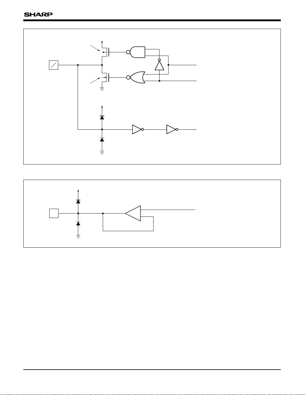
INPUT/OUTPUT CIRCUITS
I
V
CC
GND
To Internal Circuit
Fig. 1 Input Circuit (1)
¿Applicable pins¡
CK, LS, REV, LBR,
XA
0-XA7, XB0-XB7,
YA
0-YA7, YB0-YB7,
ZA
0-ZA7, ZB0-ZB7
I
V
CC
GND GND
To Internal Circuit
Fig. 2 Input Circuit (2)
¿Applicable pins¡
POLA, POLB
FUNCTIONAL OPERATIONS OF EACH BLOCK
Page 5
LH168R
5
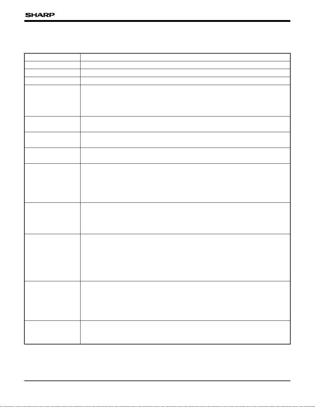
O
V
LS
GND
From Internal Circuit
Operational Amplifier
+
–
Fig. 4 Output Circuit
¿Applicable pins¡
XO
1-XO128,
YO
1-YO128,
ZO
1-ZO128
VCC
GND
Nch Tr
Output Signal
Output Control Signal
VCC
GND
To Internal Circuit
I
O
Pch Tr
Fig. 3 Input/Output Circuit
¿Applicable pins¡
SPIO, SPOI
Page 6
LH168R
6
SYMBOL FUNCTION
V
CC Used as power supply pin for digital circuit, connected to +2.5 to +3.6 V.
V
LS Used as power supply pin for analog circuit, connected to +8.0 to +13.0 V.
GND Used as ground pin, connected to 0 V.
SPIO
SPOI
Used as input pins of start pulse and also used as output pins for cascade connection.
When "H" is input into start pulse input pin, data sampling is started. On completion of
sampling, "H" pulse is output to output pin for cascade connection. Pin functions are
selected by LBR. For selecting , refer to "Functional Operations".
LBR
Used as input pin for selecting the shift register direction. For selecting, refer to
"Functional Operations".
LS
Used as input pin for parallel transfer from sampling memory to hold memory. Data is
transferred at the rising edge and output from LCD drive output pin.
CK
Used as shift clock input pin. Data is latched into sampling memory from data input pin at
the rising edge.
VH
0-VH256
VL0-VL256
Used as reference voltage input pins. Hold the reference voltage fixed during the period of
LCD drive output. For relation between input data and output voltage values, refer to
"Output Voltage Value". For internal gamma correction, refer to "Gamma Correction
Value". Observe the following relation for input voltage.
V
LS > VH0 ≥ VH32 ≥ π ≥ VH256 ≥ VL256 ≥ π ≥ VL32 ≥ VL0 > GND.
XA
0-XA7, YA0-YA7
ZA0-ZA7, XB0-XB7
YB0-YB7, ZB0-ZB7
Used as data input pins of R, G, and B colors. 8-bit x 2-pixel data are input from data pins
at the rising edge of CK. For relation between input data and output voltage values, refer
to "Functional Operations" and "Output Voltage Value". Select the data to be entered
into X, Y, and Z according to picture element arrays of the panel.
XO
1-XO128
YO1-YO128
ZO1-ZO128
Used as LCD drive output pins which output the voltage corresponding to the input of data
input pins (XA
0 to XA7, YA0 to YA7, ZA0 to ZA7, XB0 to XB7, YB0 to YB7, ZB0 to ZB7).
Data of XO1 to XO128 correspond to XA0 to XA7 and XB0 to XB7. Data of YO1 to YO128
correspond to YA0 to YA7 and YB0 to YB7, and data of ZO1 to ZO128 correspond to ZA0 to
ZA7 and ZB0 to ZB7. For relation between input data and output voltage values, refer to
"Functional Operations" and "Output Voltage Value".
POLA
POLB
Used as input pins for input data polarity exchange, POLA corresponds to XA
0 to XA7, YA0
to YA7 and ZA0 to ZA7, and POLB corresponds to XB0 to XB7, YB0 to YB7 and ZB0 to ZB7.
When "L" is entered, display data becomes normal mode. When "H" is entered, input data
becomes polarity exchange mode. For relation between input data and output voltage
values, refer to "Output Voltage Value". These pins are pulled down at the inside.
REV
Used as polarity exchange pin of LCD drive output. Date is taken at the term when LS is
"H" and the output polarity of the LCD drive output pin is determined. For exchanging, refer
to "Output Characteristics".
FUNCTIONAL DESCRIPTION
Pin Functions
Page 7

LH168R
7
The following describes the relation between LBR
pin, SPOI pin, SPIO pin and output direction.
Data input pin
XA0-XA7 YA0-YA7 ZA0-ZA7 XB0-XB7 YB0-YB7 ZB0-ZB7 πππ XB0-XB7 YB0-YB7 ZB0-ZB7
Output
direction
XO
1 YO1 ZO1 XO2 YO2 ZO2 πππ XO128 YO128 ZO128
NOTES :
+ : The gray scale voltages corresponding to reference voltage VH0 to VH256 are output.
– : The gray scale voltages corresponding to reference voltage VL
0 to VL256 are output.
Output Characteristics
The following describes the relation between REV
pin and output polarity of LCD drive pin.
REV "H" "L"
XO
1 +–
YO
1 –+
ZO1 +–
XO
2 –+
YO2 +–
ZO
2 –+
XO
3 +–
YO3 –+
:::
XO
126 –+
YO
126 +–
ZO126 –+
XO
127 +–
YO
127 –+
ZO127 +–
XO
128 –+
YO128 +–
ZO
128 –+
PIN
OUTPUT DIRECTION
LBR H L
SPOI Input Output
SPIO Output Input
NOTE :
Color data corresponding to X, Y, and Z vary depending on the output direction.
LEFT SHIFT (ZO128, YO128, XO128/ZO1, YO1, XO1)RIGHT SHIFT (XO1, YO1, ZO1/XO128, YO128, ZO128)
Functional Operations
The following describes the relation between data
input pin and output direction.
Page 8

LH168R
8
Output Voltage Value
Two voltages are selected from all of the reference
voltages (V
0-V256) by the upper 3-bit data (D7, D6
and D5) of the 8-bit input data (D7, D6, D5, D4, D3,
D
2, D1 and D0) taken by time sharing, and
intermediate value is determined by the lower 5-bit
data (D
4, D3, D2, D1 and D0).
The V
i is a reference voltage (VHi or VLi) that is
determined by the polarity exchange input (REV).
Relation between input data and output voltage
values is shown below.
(
i = 0, 32, 64, 96, 128, 160, 192, 224, 256)
INPUT
DATA
OUTPUT VOLTAGE
POLA (POLB) = "L" POLA (POLB) = "H"
0V0 V256 + (V224 – V256) x (0.99 – 0.99 x 6.61/8.96)/2.13
1V
32 + (V0 – V32) x 31/32 V256 + (V224 – V256) x (0.99 – 0.99 x 5.74/8.96)/2.13
2V32 + (V0 – V32) x 30/32 V256 + (V224 – V256) x (0.99 – 0.99 x 4.87/8.96)/2.13
3V
32 + (V0 – V32) x 29/32 V256 + (V224 – V256) x (0.99 – 0.99 x 4/8.96)/2.13
4V32 + (V0 – V32) x 28/32 V256 + (V224 – V256) x (0.99 – 0.99 x 3/8.96)/2.13
5V
32 + (V0 – V32) x 27/32 V256 + (V224 – V256) x (0.99 – 0.99 x 2/8.96)/2.13
6V32 + (V0 – V32) x 26/32 V256 + (V224 – V256) x (0.99 – 0.99 x 1/8.96)/2.13
7V
32 + (V0 – V32) x 25/32 V256 + (V224 – V256) x (1.44 – 0.45 x 8/8)/2.13
8V
32 + (V0 – V32) x 24/32 V256 + (V224 – V256) x (1.44 – 0.45 x 7/8)/2.13
9V32 + (V0 – V32) x 23/32 V256 + (V224 – V256) x (1.44 – 0.45 x 6/8)/2.13
AV
32 + (V0 – V32) x 22/32 V256 + (V224 – V256) x (1.44 – 0.45 x 5/8)/2.13
BV32 + (V0 – V32) x 21/32 V256 + (V224 – V256) x (1.44 – 0.45 x 4/8)/2.13
CV
32 + (V0 – V32) x 20/32 V256 + (V224 – V256) x (1.44 – 0.45 x 3/8)/2.13
DV
32 + (V0 – V32) x 19/32 V256 + (V224 – V256) x (1.44 – 0.45 x 2/8)/2.13
EV32 + (V0 – V32) x 18/32 V256 + (V224 – V256) x (1.44 – 0.45 x 1/8)/2.13
FV
32 + (V0 – V32) x 17/32 V256 + (V224 – V256) x (1.8 – 0.36 x 8/8)/2.13
10 V32 + (V0 – V32) x 16/32 V256 + (V224 – V256) x (1.8 – 0.36 x 7/8)/2.13
11 V
32 + (V0 – V32) x 15/32 V256 + (V224 – V256) x (1.8 – 0.36 x 6/8)/2.13
12 V
32 + (V0 – V32) x 14/32 V256 + (V224 – V256) x (1.8 – 0.36 x 5/8)/2.13
13 V32 + (V0 – V32) x 13/32 V256 + (V224 – V256) x (1.8 – 0.36 x 4/8)/2.13
14 V
32 + (V0 – V32) x 12/32 V256 + (V224 – V256) x (1.8 – 0.36 x 3/8)/2.13
15 V32 + (V0 – V32) x 11/32 V256 + (V224 – V256) x (1.8 – 0.36 x 2/8)/2.13
16 V
32 + (V0 – V32) x 10/32 V256 + (V224 – V256) x (1.8 – 0.36 x 1/8)/2.13
17 V
32 + (V0 – V32) x 9/32 V256 + (V224 – V256) x (2.13 – 0.33 x 8/8)/2.13
18 V32 + (V0 – V32) x 8/32 V256 + (V224 – V256) x (2.13 – 0.33 x 7/8)/2.13
19 V
32 + (V0 – V32) x 7/32 V256 + (V224 – V256) x (2.13 – 0.33 x 6/8)/2.13
1A V32 + (V0 – V32) x 6/32 V256 + (V224 – V256) x (2.13 – 0.33 x 5/8)/2.13
1B V
32 + (V0 – V32) x 5/32 V256 + (V224 – V256) x (2.13 – 0.33 x 4/8)/2.13
1C V32 + (V0 – V32) x 4/32 V256 + (V224 – V256) x (2.13 – 0.33 x 3/8)/2.13
1D V
32 + (V0 – V32) x 3/32 V256 + (V224 – V256) x (2.13 – 0.33 x 2/8)/2.13
1E V
32 + (V0 – V32) x 2/32 V256 + (V224 – V256) x (2.13 – 0.33 x 1/8)/2.13
1F V32 + (V0 – V32) x 1/32 V224
Page 9

9
LH168R
INPUT
DATA
OUTPUT VOLTAGE
POLA (POLB) = "L" POLA (POLB) = "H"
20 V32 V224 + (V192 – V224) x 1/32
21 V
64 + (V32 – V64) x 31/32 V224 + (V192 – V224) x 2/32
22 V64 + (V32 – V64) x 30/32 V224 + (V192 – V224) x 3/32
:: :
3D V
64 + (V32 – V64) x 3/32 V224 + (V192 – V224) x 30/32
3E V
64 + (V32 – V64) x 2/32 V224 + (V192 – V224) x 31/32
3F V64 + (V32 – V64) x 1/32 V192
40 V64 V192 + (V160 – V192) x 1/32
41 V
96 + (V64 – V96) x 31/32 V192 + (V160 – V192) x 2/32
42 V96 + (V64 – V96) x 30/32 V192 + (V160 – V192) x 3/32
:: :
5D V
96 + (V64 – V96) x 3/32 V192 + (V160 – V192) x 30/32
5E V
96 + (V64 – V96) x 2/32 V192 + (V160 – V192) x 31/32
5F V
96 + (V64 – V96) x 1/32 V160
60 V96 V160 + (V128 – V160) x 1/32
61 V
128 + (V96 – V128) x 31/32 V160 + (V128 – V160) x 2/32
62 V128 + (V96 – V128) x 30/32 V160 + (V128 – V160) x 3/32
:: :
7D V
128 + (V96 – V128) x 3/32 V160 + (V128 – V160) x 30/32
7E V128 + (V96 – V128) x 2/32 V160 + (V128 – V160) x 31/32
7F V
128 + (V96 – V128) x 1/32 V128
80 V128 V128 + (V96 – V128) x 1/32
81 V
160 + (V128 – V160) x 31/32 V128 + (V96 – V128) x 2/32
82 V
160 + (V128 – V160) x 30/32 V128 + (V96 – V128) x 3/32
:: :
9D V
160 + (V128 – V160) x 3/32 V128 + (V96 – V128) x 30/32
9E V160 + (V128 – V160) x 2/32 V128 + (V96 – V128) x 31/32
9F V
160 + (V128 – V160) x 1/32 V96
A0 V160 V96 + (V64 – V96) x 1/32
A1 V
192 + (V160 – V192) x 31/32 V96 + (V64 – V96) x 2/32
A2 V
192 + (V160 – V192) x 30/32 V96 + (V64 – V96) x 3/32
:: :
BD V
192 + (V160 – V192) x 3/32 V96 + (V64 – V96) x 30/32
BE V192 + (V160 – V192) x 2/32 V96 + (V64 – V96) x 31/32
BF V
192 + (V160 – V192) x 1/32 V64
C0 V192 V64 + (V32 – V64) x 1/32
C1 V224 + (V192 – V224) x 31/32 V64 + (V32 – V64) x 2/32
C2 V
224 + (V192 – V224) x 30/32 V64 + (V32 – V64) x 3/32
:: :
DD V
224 + (V192 – V224) x 3/32 V64 + (V32 – V64) x 30/32
DE V
224 + (V192 – V224) x 2/32 V64 + (V32 – V64) x 31/32
DF V224 + (V192 – V224) x 1/32 V32
Page 10

10
LH168R
INPUT
DATA
OUTPUT VOLTAGE
POLA (POLB) = "L" POLA (POLB) = "H"
E0 V224 V32 + (V0 – V32) x 1/32
E1 V
256 + (V224 – V256) x (2.13 – 0.33 x 1/8)/2.13 V32 + (V0 – V32) x 2/32
E2 V256 + (V224 – V256) x (2.13 – 0.33 x 2/8)/2.13 V32 + (V0 – V32) x 3/32
E3 V
256 + (V224 – V256) x (2.13 – 0.33 x 3/8)/2.13 V32 + (V0 – V32) x 4/32
E4 V256 + (V224 – V256) x (2.13 – 0.33 x 4/8)/2.13 V32 + (V0 – V32) x 5/32
E5 V
256 + (V224 – V256) x (2.13 – 0.33 x 5/8)/2.13 V32 + (V0 – V32) x 6/32
E6 V256 + (V224 – V256) x (2.13 – 0.33 x 6/8)/2.13 V32 + (V0 – V32) x 7/32
E7 V
256 + (V224 – V256) x (2.13 – 0.33 x 7/8)/2.13 V32 + (V0 – V32) x 8/32
E8 V
256 + (V224 – V256) x (2.13 – 0.33 x 8/8)/2.13 V32 + (V0 – V32) x 9/32
E9 V256 + (V224 – V256) x (1.8 – 0.36 x 1/8)/2.13 V32 + (V0 – V32) x 10/32
EA V
256 + (V224 – V256) x (1.8 – 0.36 x 2/8)/2.13 V32 + (V0 – V32) x 11/32
EB V256 + (V224 – V256) x (1.8 – 0.36 x 3/8)/2.13 V32 + (V0 – V32) x 12/32
EC V
256 + (V224 – V256) x (1.8 – 0.36 x 4/8)/2.13 V32 + (V0 – V32) x 13/32
ED V
256 + (V224 – V256) x (1.8 – 0.36 x 5/8)/2.13 V32 + (V0 – V32) x 14/32
EE V256 + (V224 – V256) x (1.8 – 0.36 x 6/8)/2.13 V32 + (V0 – V32) x 15/32
EF V
256 + (V224 – V256) x (1.8 – 0.36 x 7/8)/2.13 V32 + (V0 – V32) x 16/32
F0 V256 + (V224 – V256) x (1.8 – 0.36 x 8/8)/2.13 V32 + (V0 – V32) x 17/32
F1 V
256 + (V224 – V256) x (1.44 – 0.45 x 1/8)/2.13 V32 + (V0 – V32) x 18/32
F2 V
256 + (V224 – V256) x (1.44 – 0.45 x 2/8)/2.13 V32 + (V0 – V32) x 19/32
F3 V256 + (V224 – V256) x (1.44 – 0.45 x 3/8)/2.13 V32 + (V0 – V32) x 20/32
F4 V
256 + (V224 – V256) x (1.44 – 0.45 x 4/8)/2.13 V32 + (V0 – V32) x 21/32
F5 V256 + (V224 – V256) x (1.44 – 0.45 x 5/8)/2.13 V32 + (V0 – V32) x 22/32
F6 V
256 + (V224 – V256) x (1.44 – 0.45 x 6/8)/2.13 V32 + (V0 – V32) x 23/32
F7 V
256 + (V224 – V256) x (1.44 – 0.45 x 7/8)/2.13 V32 + (V0 – V32) x 24/32
F8 V256 + (V224 – V256) x (1.44 – 0.45 x 8/8)/2.13 V32 + (V0 – V32) x 25/32
F9 V
256 + (V224 – V256) x (0.99 – 0.99 x 1/8.96)/2.13 V32 + (V0 – V32) x 26/32
FA V256 + (V224 – V256) x (0.99 – 0.99 x 2/8.96)/2.13 V32 + (V0 – V32) x 27/32
FB V
256 + (V224 – V256) x (0.99 – 0.99 x 3/8.96)/2.13 V32 + (V0 – V32) x 28/32
FC V256 + (V224 – V256) x (0.99 – 0.99 x 4/8.96)/2.13 V32 + (V0 – V32) x 29/32
FD V
256 + (V224 – V256) x (0.99 – 0.99 x 4.87/8.96)/2.13 V32 + (V0 – V32) x 30/32
FE V
256 + (V224 – V256) x (0.99 – 0.99 x 5.74/8.96)/2.13 V32 + (V0 – V32) x 31/32
FF V256 + (V224 – V256) x (0.99 – 0.99 x 6.61/8.96)/2.13 V0
Page 11

11
LH168R
‹ (Gamma) Correction Value
Between reference voltage input pins VH0 and
VH
256, 256 resistors are connected in series. And
between reference voltage input pins VL
0 and
VL
256, 256 resistors are connected in series. No
resistor is connected between reference voltage
input pins VH
256 and VL256.
The ‹ correction curve is a broken line connected
between intermediate voltage inputs (VH
32, VH64,
VH
96, VH128, VH160, VH192, VH224, VL32, VL64,
VL
96, VL128, VL160, VL192 and VL224). Each ‹
correction value between the intermediate voltage
inputs is divided into 32 parts by resistor.
External Reference Voltage
VH0
VH32
R0
R1
VH64
VH96
R2
32 equal parts
32 equal parts
32 equal parts
LH168R
R3
VH128
VH160
R4
32 equal parts
32 equal parts
R5
VH192
VH224
R6
32 equal parts
32 equal parts
R82
R83
R81
VL224
R80
8 equal parts
8 parts
8 equal parts
8 equal parts
R9
VL192
VL160
R10
32 equal parts
32 equal parts
R11
VL128
VL96
R12
32 equal parts
32 equal parts
32 equal parts
32 equal parts
32 equal parts
R13
VL64
VL32
R14
R15
VL0
R70
R71
8 equal parts
8 equal parts
R72
8 equal parts
VH256
VL256
R73
8 parts
Page 12

12
LH168R
R73
1.00
1.00
1.00
1.00
0.87
0.87
0.87
2.35
The following shows the ratio of ‹ correction resistance of R73 and R83, when R730 equals 1.
R737 (VH256 side)
R
736
R735
R734
R733
R732
R731
R730
R83
2.35
0.87
0.87
0.87
1.00
1.00
1.00
1.00R
830
R831
R832
R833
R834
R835
R836
R837 (VL256 side)
R0
The following shows the ratio of ‹ correction resistance, when R0 equals 1.
0.33
1.00
0.74
0.60
0.52
0.49
0.60
1.00 R
83
0.52
0.60
0.74
1.00
0.33
0.36
0.45
0.99
R
1
R2
R3
R4
R5
R6
R70
R82
R81
R80
R9
R10
R11
R12
R73 0.99
R
72 0.45
R71 0.36
R
15 1.00
R
14 0.60
R13 0.49
PRECAUTIONS
Precautions when connecting or disconnecting
the power supply
This IC has some power supply pins, so it may be
permanently damaged by a high current which may
flow if voltage is supplied to the LCD drive power
supply while the logic system power supply is
floating. Therefore, when connecting the power
supply, observe the following sequence.
V
CC / logic input / VLS, VH0-VH256, VL0-VL256
When disconnecting the power supply, follow the
reverse sequence.
Reference voltage input
The relation of the reference voltage input is shown
here.
V
LS > VH0 ≥ VH32 ≥ π ≥ VH224 ≥ VH256 ≥ 0.5VLS
≥ VL256 ≥ VL224 ≥ π ≥ VL32 ≥ VL0 > GND
Maximum ratings
When connecting or disconnecting the power
supply, this IC must be used within the range of the
absolute maximum ratings.
Target output load
This IC is designed for a 200 pF output load
capacity. When using this IC for other than 200 pF
panels, confirm the device is having no problem
before using it.
Page 13

LH168R
13
RECOMMENDED OPERATING CONDITIONS
PARAMETER SYMBOL APPLICABLE PINS RATING UNIT NOTE
Supply voltage
V
CC VCC –0.3 to +6.0 V
1, 2
V
LS VLS –0.3 to +14.0 V
Input voltage
VI VH0-VL0 –0.3 to VLS + 0.3 V
Storage temperature T
STG –45 to +125 ˚C
NOTES :
1. TA = +25 ˚C
2. The maximum applicable voltage on any pin with respect to GND (0 V).
NOTE :
1. The applicable voltage on any pin with respect to GND (0 V).
PARAMETER SYMBOL MAX. UNIT NOTE
Supply voltage
V
CC
1
Reference voltage input
VH
0-VH256
VLS – 0.2
V
Clock frequency f
CK 65 MHz
MIN. TYP.
+2.5
0.5V
CC
VLS
VI
SPIO, SPOI, CK, LS, REV,
LBR, POLA, POLB, XA0-XA7,
XB
0
-XB7, YA0-YA7, YB0-YB7,
ZA0-ZA7, ZB0-ZB
7
–0.3 to VCC + 0.3 V
V–0.3 to V
LS + 0.3
XO1-ZO
128
VO
V–0.3 to VCC + 0.3SPIO, SPOIVO
Output voltage
+3.6 V
+8.0 +13.0 V
–20 ˚C+75TOPROperating temperature
pF200C
L
LCD drive output load capacity
VL0-VL256 +0.2 0.5VCC V
ABSOLUTE MAXIMUM RATINGS
Page 14

LH168R
14
ELECTRICAL CHARACTERISTICS
DC Characteristics
(VCC = +2.5 to +3.6 V, VLS = +8.0 to +13.0 V, TOPR = –20 to +75 ˚C)
PARAMETER
SYMBOL
CONDITIONS APPLICABLE PINS MIN. TYP. MAX. UNIT. NOTE
Input "Low" voltage V
IL
XA0-XA7, YA0-YA7, ZA0-ZA7,
XB
0-XB7, YB0-YB7, ZB0-ZB7,
SPIO, SPOI, CK, LS, LBR,
REV, POLA, POLB
GND 0.3VCC V
V
IH 0.7VCC VCC V
Input "High" current
I
ILH1
XA0-XA7, YA0-YA7, ZA0-ZA7,
XB
0-XB7, YB0-YB7, ZB0-ZB7,
SPIO, SPOI, CK, LS, LBR,
REV
10 µA
Supply current
(In operation mode)
I
CC1
fCK = 65 MHz
f
LS = 50 kHz
(Data sampling state)
VCC-GND 14 mA
Supply current
(In standby mode)
I
CC2
fCK = 65 MHz
fLS = 50 kHz
SPI = GND is fixed.
(Standby state)
V
CC-GND 1.5 mA
Supply current
(In operation mode)
I
LS1
fCK = 65 MHz
f
LS = 50 kHz
(Data sampling state)
VLS-GND
Output voltage range V
OUT
XO1-ZO128
GND + 0.2
VLS – 0.2
V
1Deviations between
output voltage pins
V
OD –10 +10 mV
Output current I
O1-IO4 200 µA 2
Resistance between
reference voltage input pins
RGMAH VH0-VH256 20 k$
µA10
XA0-XA7, YA0-YA7, ZA0-ZA7,
XB0-XB7, YB0-YB7, ZB0-ZB7,
SPIO, SPOI, CK, LS, LBR,
REV, POLA, POLB
IILL1Input "Low" current
VV
CC
VCC – 0.4
IOH = –0.3 mAVOH
V
GND + 0.4
GND
SPIO, SPOI
IOL = 0.3 mAVOLOutput "Low" voltage
Input "High" voltage
Output "H" voltage
5mA
mA4V
LS-GND
f
CK = 65 MHz
fLS = 50 kHz
SPI = GND is fixed.
(Standby state)
I
LS2
Supply current
(In standby mode)
I
ILH2 POLA, POLB 400 µA
R
GMAL k$20VL0-VL256
Page 15

LH168R
15
NOTES :
1. Criterion of evaluating voltage deviations.
(a) Between output voltage pins
Measuring values : Output voltage value at the time after
10 µs at the rising edge of LS.
(Average of several times)
(Conditions) Output load capacity is 200 pF.
In a state when the reference voltage is fixed.
Expecting values : Calculated following these specifications.
(Conditions) In a state when the reference voltage is fixed.
(b) Between LCD drivers
Measuring values : Applicable to (a).
(Conditions) Applicable to (a).
Expecting values : Applicable to (a).
(Conditions) Applicable to (a).
Each input voltage between the LCD drivers must be
made perfectly equal by connecting corresponding
reference voltage input pins.
2. I
O1 : Applied voltage = 8.0 V for output pins XO1 to ZO128.
Output voltage = 7.5 V for output pins XO
1 to ZO128.
V
LS = 10.0 V
I
O2 : Applied voltage = 7.0 V for output pins XO1 to ZO128.
Output voltage = 7.5 V for output pins XO
1 to ZO128.
V
LS = 10.0 V
I
O3 : Applied voltage = 3.0 V for output pins XO1 to ZO128.
Output voltage = 2.5 V for output pins XO
1 to ZO128.
V
LS = 10.0 V
I
O4 : Applied voltage = 2.0 V for output pins XO1 to ZO128.
Output voltage = 2.5 V for output pins XO
1 to ZO128.
V
LS = 10.0 V
Page 16

16
LH168R
AC Characteristics (VCC = +2.5 to +2.7 V, VLS = +8.0 to +13.0 V, TOPR = –20 to +75 ˚C)
PARAMETER
SYMBOL
CONDITIONS APPLICABLE PINS MIN. TYP. MAX. UNIT
Clock frequency f
CK
CK
40 MHz
"H" level pulse width tCWH 8ns
Input rise time t
CR 10 ns
Input fall time tCF 10 ns
Data setup time t
SUD
XA0-XA7, YA0-YA7, ZA0-ZA7,
XB0-XB7, YB0-YB7, ZB0-ZB7,
POLA, POLB
6ns
Data hold time t
HD 6ns
Start pulse setup time t
SUSP 6ns
Start pulse hold time tHSP 6ns
Start pulse output
delay time
t
DSP CL = 15 pF 19 ns
LCD drive output
delay time 1
t
DO1 3µs
LCD drive output
delay time 2
t
DO2 10 µs
SPIO, SPOI
ns8tCWL"L" level pulse width
ns
1
-------f
CK
tWSPStart pulse width
ns7t
HLS
LS signal-CK signal
hold time
ns
1
-------f
CK
tLSSP
LS signal-SPI signal
setup time
C
L = 200 pF
C
L = 200 pF
XO1-ZO128
LS
LS signal "H" level
width
t
WLS
1
-------f
CK
ns
ns10t
HRV
REV signal-LS signal
hold time
ns14t
SURV
REV signal-LS signal
setup time
REV
Page 17

17
LH168R
(VCC = +2.7 to +3.6 V, VLS = +8.0 to +13.0 V, TOPR = –20 to +75 ˚C)
PARAMETER
SYMBOL
CONDITIONS APPLICABLE PINS MIN. TYP. MAX. UNIT
Clock frequency f
CK
CK
65 MHz
"H" level pulse width tCWH 4ns
Input rise time t
CR 10 ns
Input fall time tCF 10 ns
Data setup time t
SUD
XA0-XA7, YA0-YA7, ZA0-ZA7,
XB0-XB7, YB0-YB7, ZB0-ZB7,
POLA, POLB
4ns
Data hold time t
HD 1ns
Start pulse setup time t
SUSP 3ns
Start pulse hold time tHSP 2ns
Start pulse output
delay time
t
DSP CL = 15 pF 11 ns
LCD drive output
delay time 1
t
DO1 3µs
LCD drive output
delay time 2
t
DO2 10 µs
SPIO, SPOI
ns4tCWL"L" level pulse width
ns
1
-------f
CK
tWSPStart pulse width
ns7t
HLS
LS signal-CK signal
hold time
ns
1
-------f
CK
tLSSP
LS signal-SPI signal
setup time
C
L = 200 pF
C
L = 200 pF
XO1-ZO128
LS
LS signal "H" level
width
t
WLS
1
-------f
CK
ns
ns10t
HRV
REV signal-LS signal
hold time
ns14t
SURV
REV signal-LS signal
setup time
REV
Page 18

18
LH168R
CK
LAST – 1 LAST
CK
LS
XO
1-ZO128
REV
XA
0-XA7
ZA0-ZA7
YA0-YA7
XB0-XB7
ZB0-ZB7
YB0-YB7
SPIO Input
(SPOI)
SPIO Output
(SPOI)
SPIO Input
(SPOI)
1
f
CK
21
12
tc
WH tcWL
tSUSP tHSP
tWSP
tDSP
tHLS
tWLS
tLSSP
tHRV
tDO1
Target voltage ±(VLS x 0.1)
Target voltage (8-bit accuracy)
t
DO2
tSURV
tSUD tHD
tCR tCF
POLA
POLB
Timing Chart
Page 19

PACKAGES FOR LCD DRIVERS
19
ZA5
8.0
(
SL
)
3.98
±0.2
(SR
)
[6.18 (E.L.)]
5.08
±0.05
[2.2
TYP.
(
2.0
MIN.
)
]
[0.3]
[1.225]
[1.65]
[1.1]
[0.45]
0.05
0.1
±0.02
0.05
[2.2
TYP.
(
2.0
MIN.
)
]
[0.1]
0.75
0.6 (SL
)
VCOM
R20
R21
VCOM
VCOM
ZO1
DUMMY
DUMMY
DUMMY
XO1
YO1
13.35
(
SR
)
ZO128
YO128
XO128
13.35
(
SR
)
(
Good device hole
)
2.9(SL
)
9.32(SL
)
9.62
±0.5
4.6(SL
)
6.32
±0.2
(SR
)
[14.5 (E.L.)]
2.88 (SL
)
1.7(SL
)
3.5
±0.05
(Holes)
4.1
±0.05
(Holes)
[8.32(E.L.)]
7.32 (SL
)
0.8 (SL
)
0.5 (SL
)
Ø1.0
XO1
1.5
(
SL
)
4.0
(
SL
)
12.7
(
SL
)
10.5
±0.5
ZO128
4.6
(
SL
)
4.6
(
SL
)
12.7
(
SL
)
YA4
DUMMY
R20
R21
VCOM
GND
VLS
GND
0.6
(
SL
)
XA0
XB0
YA5
YA6
YA7
XA1
XA2
XA3
XA4
XA5
XA6
XA7
XB1
XB2
XB3
XB4
XB5
XB6
XB7
13.5
(
SL
)
13.6
±0.2
(
SR
)
REV
VL128
VL192
VL256
VH256
VH192
VH128
VH64
VH0
SPOI
YA0
YA1
YA2
YA3
VL0
VL64
LS
SPIO
CK
YB7
ZA6
ZB1
ZB2
ZB3
ZB4
ZB5
ZB6
ZB7
YB1
YB2
YB3
YB4
YB5
YB6
ZA7
ZB0
YB0
13.6
±0.2
(
SR
)
13.5
(
SL
)
(Backside PI coating)
4.75
±0.05
1.42
±0.05
0.6
(MAX.)
Backside
Total
1.0
MAX.
0.75
MAX.
VCOM
VCOM
VCOM
DUMMY
DUMMY
DUMMY
R10
R11
Pattern side
0.2
MAX.
(Backside PI coating)
0.4
±0.2
1.42
±0.05
1.0
(Backside PI coating)
0.6
(MAX.)
2-R0.6
(
SR
)
2-Ø0.6
(
Cu hole
)
VCOM
R10
R11
ZA1
ZA2
ZA3
ZA4
GND
VLS
VCC
LBR
ZA0
2-Ø0.6
(
PI
)
2-Ø0.9
(
Cu
)
2-R0.8
(
Cu
)
2-Ø1.0
(
PI
)
Device center
Film center
Sprocket center
Chip center
0.6
(
SL
)
1.5
(
SL
)
(Resin area)
5.8
MAX.
P0.065 x
(
400 – 1
)
– 0.028 = 25.907
±0.035
W0.033
±0.015
28.0
20.4
MAX.
(Resin area)
26.6
(
SL
)
[27.6
(
E.L.
)
]
34.975
P0.35 x (77 – 1
) =
26.6
±0.04
W0.15
±0.02
21.4
±0.05
(Holes)
25.0
±0.05
(Holes)
[27.6
(
E.L.
)
]
31.82
8.0
(
SL
)
LH168R01
Tape width
ø Tape Specification ø Tape Material
35 mm
Tape type
Super wide
Perforation pitch
4 pitches
Substrate UPILEX S75
Adhesive #7100
Cu foil [thickness]
FQ-VLP 15 µm
Solder resist Poly urethane SSF
PACKAGE (Unit : mm)
UPILEX is a trademark of UBE INDUSTRIES, LTD..
 Loading...