

Page 1
In the absence of confirmation by device specification sheets, SHARP takes no responsibility for any defects that may occur in equipment using any SHARP devices shown in
catalogs, data books, etc. Contact SHARP in order to obtain the latest device specification sheets before using any SHARP device.
1
DESCRIPTION
The LH168P is a 309-output TFT-LCD source
driver IC which can simultaneously display 262 144
colors in 64 gray scales.
FEATURES
• Selectable number of LCD drive outputs : 309/300
• Built-in 6-bit digital input DAC
• Possible to display 262 144 colors in 64 gray
scales with reference voltage input of 11 gray
scales : This reference voltage input corresponds
to ‹ correction and intermediate reference voltage
input can be abbreviated
• Cascade connection
• Sampling sequence :
Output shift direction can be selected
XO
1, YO1, ZO1/XO103, YO103, ZO103 or
ZO
103, YO103, XO103/ZO1, YO1, XO1
• Shift clock frequency : 55 MHz (MAX.)
• Supply voltages
–V
CC (for logic system) : +3.0 to +5.5 V
–V
LS (for LCD drive system) : +3.0 to +5.5 V
• Package : 350-pin TCP (Tape Carrier Package)
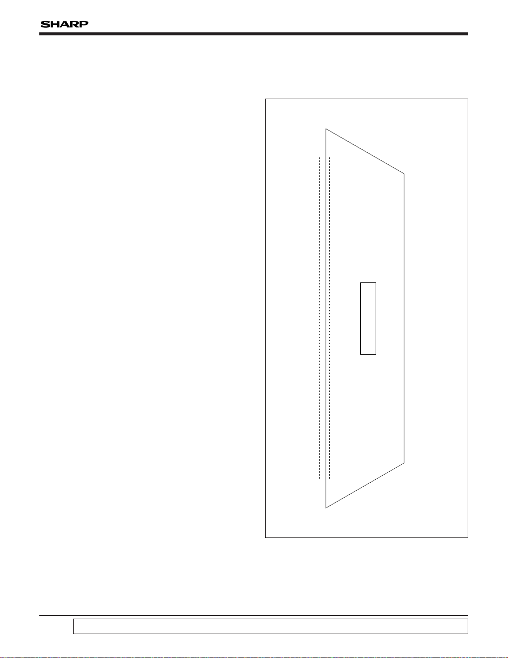
PIN CONNECTIONS
LH168P
LH168P
309-output TFT-LCD Source Driver IC
XO103
YO103
ZO103
307
308
309
XO
1
YO1
ZO1
1
2
3
CHIP SURFACE
GND
VLS
V9
V7
V5
V3
V1
XI5
XI4
XI3
XI2
XI1
XI0
YI5
YI4
YI3
YI2
YI1
YI0
SPOI
GND
MODE
CK
VCC
SPIO
LS
ZI5
ZI4
ZI3
ZI2
ZI1
ZI0
LBR
V0
V2
V4
V6
V8
V10
VLS
GND
350
349
348
347
346
345
344
343
342
341
340
339
338
337
336
335
334
333
332
331
330
329
328
327
326
325
324
323
322
321
320
319
318
317
316
315
314
313
312
311
310
350-PIN TCP
TOP VIEW
NOTE :
Doesn't prescribe TCP outline.
Page 2
2
LH168P
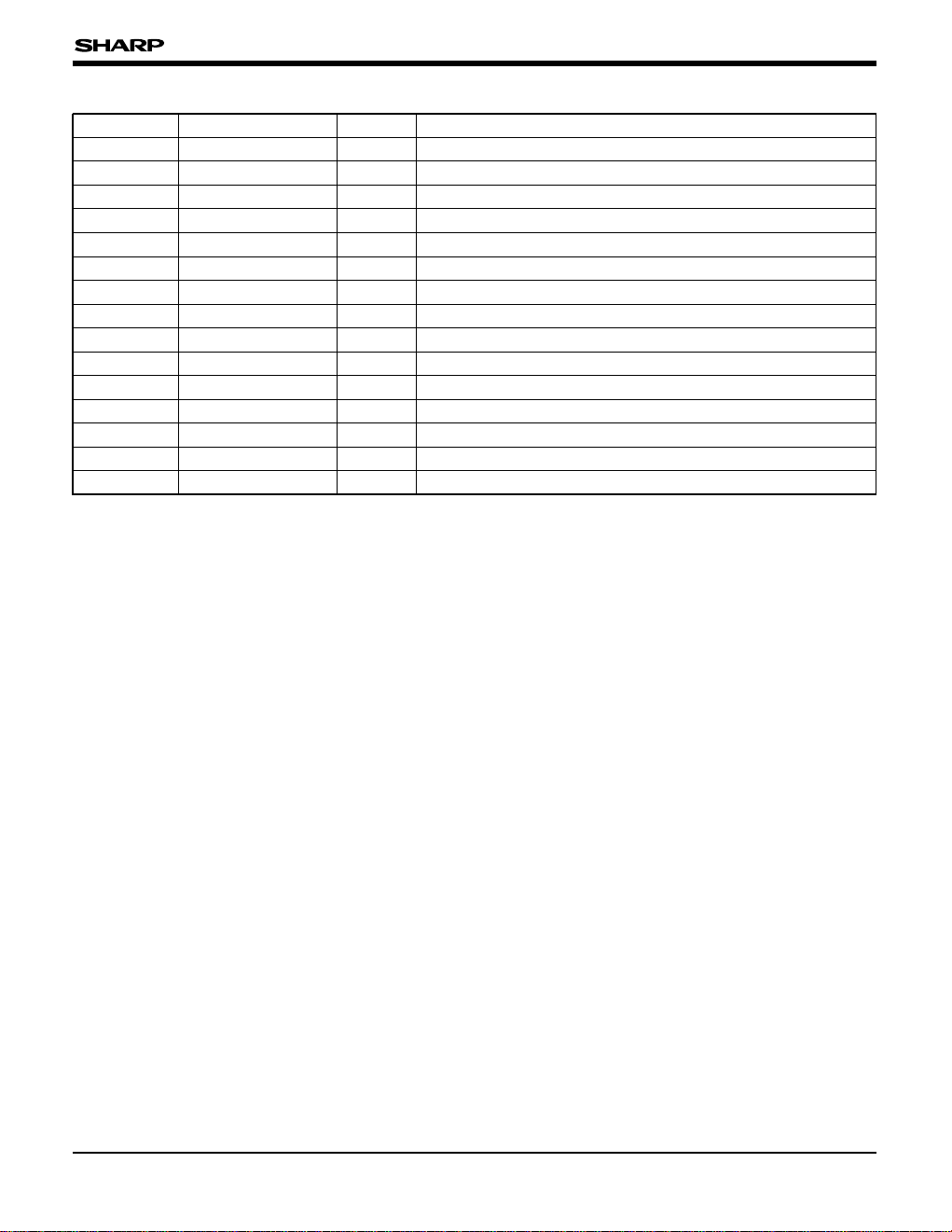
PIN DESCRIPTION
PIN NO. SYMBOL I/O DESCRIPTION
1 to 309 XO
1-ZO103 O LCD drive output pins
310, 330, 350 GND – Ground pins
311, 349 V
LS – Power supply pins for analog circuit
312 to 317 V
10, V8, V6, V4, V2, V0 I Reference voltage input pins
318 LBR I Shift direction selection input pin
319 to 324 ZI
0-ZI5 I Data input pins
325 LS I Latch input pin
326 SPIO I/O Start pulse input/cascade output pin
327 V
CC – Power supply pin for digital circuit
328 CK I Shift clock input pin
329 MODE I 309/300-output selection input pin
331 SPOI I/O Start pulse input/cascade output pin
332 to 337 YI
0-YI5 I Data input pins
338 to 343 XI
0-XI5 I Data input pins
344 to 348 V1, V3, V5, V7, V9 I Reference voltage input pins
Page 3
LH168P
3
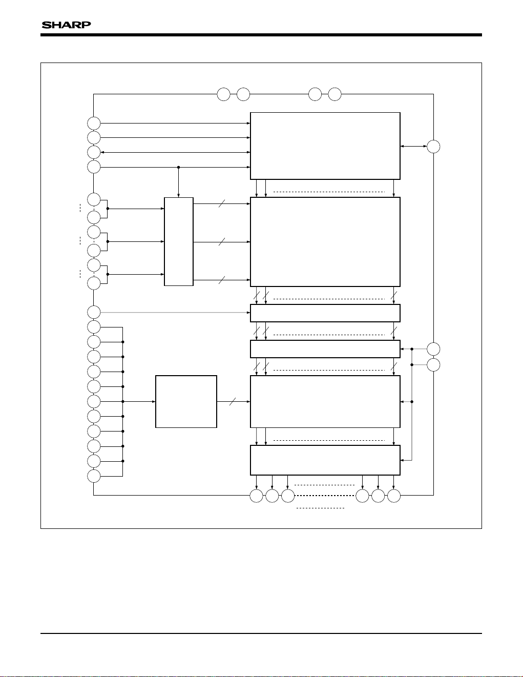
BLOCK DIAGRAM
CK 328
YI0 332
XI5
LS
343
XI0 338
SPOI 331
LBR 318
MODE 329
V0 317
V
1
V2
V3
V4
V5
V6
V7
V8
V9
V10 312
1
ZI0 319
YI5 337
ZI5 324
325
307
311
326
330327
350310
SPIO
V
LS
349 VLS
XO1
2
YO
1
3
ZO
1 XO103
308
YO
103
309
ZO
103
6
6
6
6
6
6
64
6
6
6
6
10321
6
6
V
CC GND GND GND
SHIFT REGISTER
SAMPLING MEMORY
HOLD MEMORY
DATA
LATCH
REFERENCE
VOLTAGE
GENERATION
CIRCUIT
LEVEL SHIFTER
DA CONVERTER
OUTPUT CIRCUIT
344
316
345
315
346
314
347
313
348
Page 4
FUNCTIONAL OPERATIONS OF EACH BLOCK
BLOCK FUNCTION
Shift Register
Used as a bi-directional shift register which performs the shifting operation by CK and
selects bits for data sampling.
Data Latch Used to temporary latch the input data which is sent to the sampling memory.
Sampling Memory Used to sample the data to be entered by time sharing.
Hold Memory Used for latch processing of data in the sampling memory by LS input.
Level Shifter
Used to shift the data in the hold memory to the power supply level of the analog circuit
unit and sends the shifted data to DA converter.
Reference Voltage
Generation Circuit
Used to generate a gamma-corrected 64-level voltage by the resistor dividing circuit.
DA Converter
Used to generate an analog signal according to the display data and sends the signal to
the output circuit.
Output Circuit
Used as a voltage follower, configured with an operational amplifier and an output buffer,
which outputs analog signals of 64 gray scales to LCD drive output pin.
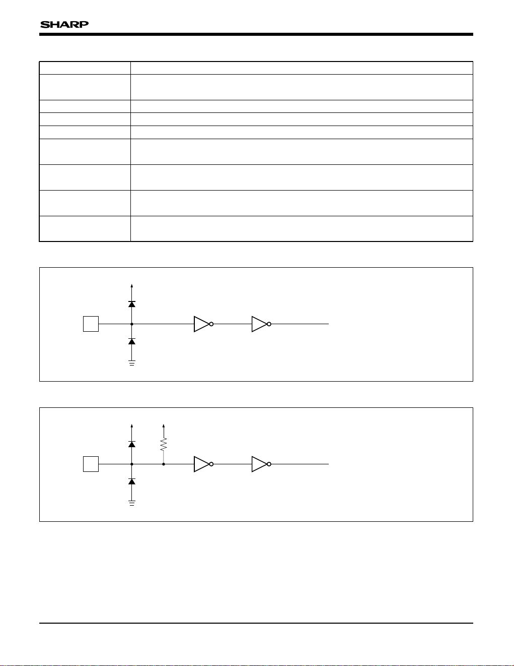
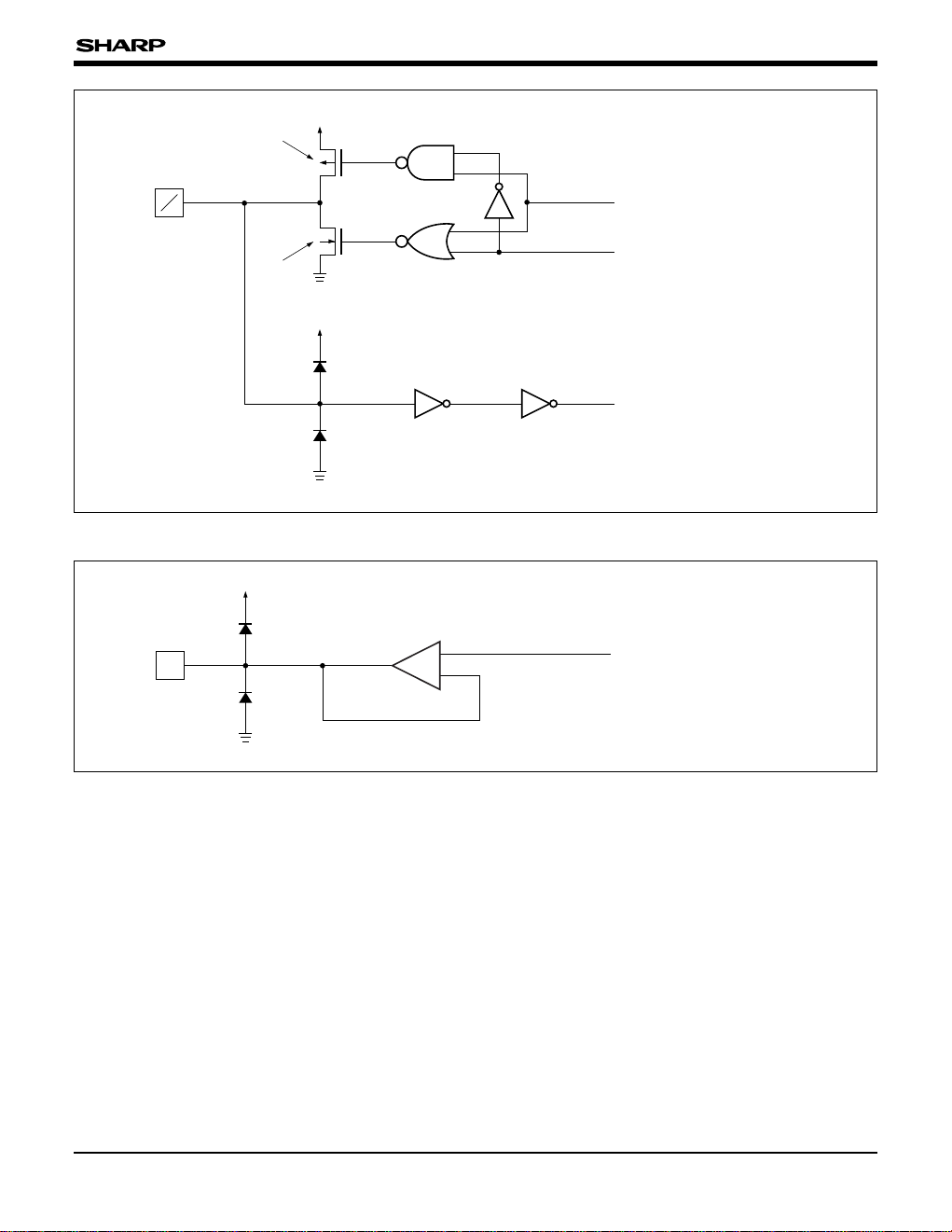
INPUT/OUTPUT CIRCUITS
I
V
CC
GND
To Internal Circuit
Fig. 1 Input Circuit (1)
¿Applicable pins¡
CK, LS, LBR, XI0-XI5,
YI
0-YI5, ZI0-ZI5
I
V
CC VCC
GND
To Internal Circuit
Fig. 2 Input Circuit (2)
¿Applicable pin¡
MODE
LH168P
4
Page 5
LH168P
5
VCC
GND
Output Signal
Output Control Signal
VCC
GND
To Internal Circuit
I
O
Nch Tr
Pch Tr
Fig. 3 Input/Output Circuit
¿Applicable pins¡
SPIO, SPOI
O
V
LS
GND
From Internal Circuit
Operational Amplifier
+
–
Fig. 4 Output Circuit
¿Applicable pins¡
XO
1-XO103,
YO
1-YO103,
ZO
1-ZO103
Page 6

6
LH168P
SYMBOL FUNCTION
V
CC Used as power supply pin for digital circuit, connected to +3.0 to +5.5 V.
V
LS Used as power supply pin for analog circuit, connected to +3.0 to +5.5 V.
GND Used as ground pin, connected to 0 V.
SPIO
SPOI
Used as input pins of start pulse and also used as output pins for cascade connection.
When "H" is input into start pulse input pin, data sampling is started. On completion of
sampling, "H" pulse is output to output pin for cascade connection. Pin functions are
selected by LBR. For selecting, refer to "Functional Operations".
LBR
Used as input pin for selecting the shift register direction. For selecting, refer to
"Functional Operations".
LS
Used as input pin for parallel transfer from sampling memory to hold memory. Data is
transferred at the rising edge and output from LCD drive output pin.
CK
Used as shift clock input pin. Data is latched into sampling memory from data input pin at
the rising edge.
V
0-V10
Used as reference voltage input pins. Hold the reference voltage fixed during the period of
LCD drive output. For relation between input data and output voltage values, refer to
"Output Voltage Value". For internal gamma correction, refer to "Gamma Correction
Value".
MODE
Used as input pin for selecting the number of LCD drive outputs (309 outputs or 300 outputs).
When "L" is entered, it is 309-output mode. When "H" is entered, it is 300-output mode.
This pin is pulled up at the inside.
Used as data input pins of R, G, and B colors. 6-bit data are input from data pins at the
rising edge of CK. For relation between input data and output voltage values, refer to
"Output Voltage Value". Select the data to be entered into X, Y, and Z according to
picture element arrays of the panel.
XI
0-XI5
YI0-YI5
XI0-ZI5
Used as LCD drive output pins which output the voltage corresponding to the data input
pins (XI
0 to XI5, YI0 to YI5, ZI0 to ZI5).
When 300-output mode, 9 output pins (XO51 to XO53, YO51 to YO53, ZO51 to ZO53) are
invalid. Invalid output pins must be opened.
Data of XO
1 to XO103 correspond to XI0 to XI5. Data of YO1 to YO103 correspond to YI0 to
YI5, and data of ZO1 to ZO103 correspond to ZI0 to ZI5.
For relation between input data and output voltage values, refer to "Functional Operations"
and "Output Voltage Value".
XO
1-XO103
YO1-YO103
ZO1-ZO103
FUNCTIONAL DESCRIPTION
Pin Functions
Page 7

7
LH168P
Functional Operations
The following describes the relation between LBR
pin, SPOI pin, SPIO pin and output direction.
PIN
OUTPUT DIRECTION
LBR H L
SPOI Input Output
SPIO Output Input
NOTE :
Color data corresponding to X, Y, and Z vary depending on the output direction.
LEFT SHIFT (ZO103, YO103, XO103/ZO1, YO1, XO1)RIGHT SHIFT (XO1, YO1, ZO1/XO103, YO103, ZO103)
Page 8

LH168P
8
Output Voltage Value
Two voltages are selected from all of the reference
voltages (V
0-V10) by the upper 3-bit data (D5, D4
and D3) of the 6-bit input data (D5, D4, D3, D2, D1
and D0) taken by time sharing, and intermediate
value is determined by the lower 3-bit data (D
2, D1
and D0).
Relation between input data and output voltage
values is shown below.
INPUT
DATA
OUTPUT VOLTAGE
INPUT
DATA
OUTPUT VOLTAGE
0V
0 20 V6 + (V5 – V6) x 7/8
V
1 21 V6 + (V5 – V6) x 6/8
1V
2+ (V1 – V2) x 6/7 22 V6 + (V5 – V6) x 5/8
2V2+ (V1 – V2) x 5/7 23 V6 + (V5 – V6) x 4/8
3V
2+ (V1 – V2) x 4/7 24 V6 + (V5 – V6) x 3/8
4V2+ (V1 – V2) x 3/7 25 V6 + (V5 – V6) x 2/8
5V
2+ (V1 – V2) x 2/7 26 V6 + (V5 – V6) x 1/8
6V
2+ (V1 – V2) x 1/7 27 V6
7V2 28 V7 + (V6 – V7) x 7/8
8V
3+ (V2 – V3) x 7/8 29 V7 + (V6 – V7) x 6/8
9V3+ (V2 – V3) x 6/8 2A V7 + (V6 – V7) x 5/8
AV
3+ (V2 – V3) x 5/8 2B V7 + (V6 – V7) x 4/8
BV
3+ (V2 – V3) x 4/8 2C V7 + (V6 – V7) x 3/8
CV3+ (V2 – V3) x 3/8 2D V7 + (V6 – V7) x 2/8
DV
3+ (V2 – V3) x 2/8 2E V7 + (V6 – V7) x 1/8
EV3+ (V2 – V3) x 1/8 2F V7
FV3 30 V8 + (V7 – V8) x 7/8
10 V
4 + (V3 – V4) x 7/8 31 V8 + (V7 – V8) x 6/8
11 V4 + (V3 – V4) x 6/8 32 V8 + (V7 – V8) x 5/8
12 V
4 + (V3 – V4) x 5/8 33 V8 + (V7 – V8) x 4/8
13 V4 + (V3 – V4) x 4/8 34 V8 + (V7 – V8) x 3/8
14 V
4 + (V3 – V4) x 3/8 35 V8 + (V7 – V8) x 2/8
15 V4 + (V3 – V4) x 2/8 36 V8 + (V7 – V8) x 1/8
16 V
4 + (V3 – V4) x 1/8 37 V8
17 V4 38 V9 + (V8 – V9) x 6/7
18 V5 + (V4 – V5) x 7/8 39 V9 + (V8 – V9) x 5/7
19 V
5 + (V4 – V5) x 6/8 3A V9 + (V8 – V9) x 4/7
1A V5 + (V4 – V5) x 5/8 3B V9 + (V8 – V9) x 3/7
1B V
5 + (V4 – V5) x 4/8 3C V9 + (V8 – V9) x 2/7
1C V
5 + (V4 – V5) x 3/8 3D V9 + (V8 – V9) x 1/7
1D V5 + (V4 – V5) x 2/8 3E V9
1E V5 + (V4 – V5) x 1/8
1F V5 3F V10
Page 9

9
LH168P
‹ (gamma) Correction Value
Between reference voltage input pins, 7 or 8
resistors of the same resistance value are
connected in series.
When the resistance ratio between respective
reference voltage input pins matches the reference
voltages (V
1 to V9) for ‹ correction of LCD panel,
the external power supply of the intermediate
voltages (for V
1 to V9 pins) is not required.
V0
V1
R0
V2
R1
V3
R2
V4
R3
V5
R4
V6
R5
V7
R6
V8
R7
V9
R8
V10
R9
7 equal parts
8 equal parts
8 equal parts
8 equal parts
8 equal parts
8 equal parts
8 equal parts
7 equal parts
LH168P
External Reference Voltage
R9 1.05
R8 1.42
R
7 0.84
R6 0.66
R
5 0.84
R
4 0.90
R3 1.50
R
2 2.77
R1 2.00
R
0 1.00
The following shows the ratio of ‹ correction resistance, when R0 equals 1.
Page 10

10
LH168P
PRECAUTIONS
Precautions when connecting or disconnecting
the power supply
This IC has some power supply pins, so it may be
permanently damaged by a high current which may
flow if voltage is supplied to the LCD drive power
supply while the logic system power supply is
floating. Therefore, when connecting the power
supply, observe the following sequence.
V
CC / logic input / VLS, V0-V10
When disconnecting the power supply, follow the
reverse sequence.
Reference voltage input
The relation of the reference voltage input is shown
here.
GND < V
0 ≤ V1 ≤ π ≤ V9 ≤ V10 < VLS or
V
LS > V0 ≥ V1 ≥ π ≥ V9 ≥ V10 > GND
Maximum ratings
When connecting or disconnecting the power
supply, this IC must be used within the range of the
absolute maximum ratings.
Target output load
This IC is designed for a 150 pF output load
capacity. When using this IC for other than 150 pF
panels, confirm the device is having no problem
before using it.
ABSOLUTE MAXIMUM RATINGS
RECOMMENDED OPERATING CONDITIONS
PARAMETER SYMBOL APPLICABLE PINS RATING UNIT NOTE
Supply voltage
V
CC VCC –0.3 to +6.0 V
1, 2
VLS VLS –0.3 to +6.0 V
Input voltage
V
I V0-V10 –0.3 to VLS + 0.3 V
Storage temperature T
STG –45 to +125 ˚C
NOTES :
1. TA = +25 ˚C
2. The maximum applicable voltage on any pin with respect to GND (0 V).
NOTE :
1. The applicable voltage on any pin with respect to GND (0 V).
PARAMETER SYMBOL MAX. UNIT NOTE
Supply voltage
V
CC
1
Reference voltage input V
0-V10 VLS V
Clock frequency f
CK 55 MHz
MIN. TYP.
+3.0
0
V
LS
VI
SPIO, SPOI, CK, LS, MODE,
LBR, XI
0
-XI5, YI0-YI5, ZI0-ZI
5
–0.3 to VCC + 0.3 V
V–0.3 to V
LS + 0.3
XO1-ZO
80
VO
V–0.3 to VCC + 0.3SPIO, SPOIVO
Output voltage
+5.5 V
+3.0 +5.5 V
–20 ˚C+75T
OPROperating temperature
pF150C
L
LCD drive output load capacity
Page 11

11
LH168P
NOTES :
1. Criterion of evaluating voltage deviations.
(a) Between output voltage pins
Measuring values : Output voltage value at the time after
10 µs at the rising edge of LS.
(Average of several times)
(Conditions) Output load capacity is 150 pF.
In a state when the reference voltage is fixed.
Expecting values : Calculated following these specifications.
(Conditions) In a state when the reference voltage is fixed.
(b) Between LCD drivers
Measuring values : Applicable to (a).
(Conditions) Applicable to (a).
Expecting values : Applicable to (a).
(Conditions) Applicable to (a).
Each input voltage between the LCD drivers must be
made perfectly equal by connecting corresponding
reference voltage input pins.
2. I
O1 : Applied voltage = 3.0 V for output pins XO1 to ZO103.
Output voltage = 2.5 V for output pins XO
1 to ZO103.
V
CC = VLS = 5.0 V
I
O2 : Applied voltage = 2.0 V for output pins XO1 to ZO103.
Output voltage = 2.5 V for output pins XO
1 to ZO103.
V
CC = VLS = 5.0 V
PARAMETER
SYMBOL
CONDITIONS APPLICABLE PINS MIN. TYP. MAX. UNIT NOTE
Input "Low" voltage V
IL
XI0-XI5, YI0-YI5, ZI0-ZI5, SPIO,
SPOI, CK, LS, LBR, MODE
GND 0.3VCC V
V
IH 0.7VCC VCC V
Input "High" current V
ILH
XI0-XI5, YI0-YI5, ZI0-ZI5, SPIO,
SPOI, CK, LS, LBR, MODE
10 µA
Supply current
(In operation mode)
I
CC1
fCK = 55 MHz
f
LS = 50 kHz
(Data sampling state)
VCC-GND
12 mA
Supply current
(In standby mode)
I
CC2
fCK = 55 MHz
f
LS = 50 kHz
SPI = GND is fixed.
(Standby state)
4mA
Supply current
(In operation mode)
I
LS1
fCK = 55 MHz
f
LS = 50 kHz
(Data sampling state)
VLS-GND
Output voltage range V
OUT
XO1-ZO103
GND + 0.1
VLS – 0.1
V
1Deviations between
output voltage pins
V
OD –20 20 mV
Output current I
O1, IO2 20 50 µA 2
Resistance between
reference voltage input pins
RGMA V0-V10 10 20 30 k$
µA400MODEI
ILL2
µA10
XI0-XI5, YI0-YI5, ZI0-ZI5, SPIO,
SPOI, CK, LS, LBR
IILL1
Input "Low" current
VV
CC
VCC – 0.4
IOH = –0.3 mAVOH
V
GND + 0.4
GND
SPIO, SPOI
IOL = 0.3 mAVOLOutput "Low" voltage
Input "High" voltage
Output "High" voltage
8mA
mA7
f
CK = 55 MHz
f
LS = 50 kHz
SPI = GND is fixed.
(Standby state)
I
LS2
Supply current
(In standby mode)
ELECTRICAL CHARACTERISTICS
DC Characteristics
(VCC = VLS = +3.0 to +5.5 V, TOPR = –20 to +75 ˚C)
Page 12

12
LH168P
PARAMETER
SYMBOL
CONDITIONS APPLICABLE PINS MIN. TYP. MAX. UNIT
Clock frequency f
CK
CK
55 MHz
"H" level pulse width tCWH 4ns
Input rise time t
CR 10 ns
Input fall time tCF 10 ns
Data setup time t
SUD
XI0-XI5, YI0-YI5, ZI0-ZI5
4ns
Data hold time tHD 0ns
Start pulse setup time t
SUSP 4ns
Start pulse hold time t
HSP 0ns
Start pulse output
delay time
t
DSP CL = 15 pF 12 ns
LCD drive output
delay time
t
DO 10 µs
LS signal-SPI signal
setup time
t
LSSP
1
-------fCK
ns
SPIO, SPOI
ns4tCWL"L" level pulse width
ns
1
-------f
CK
tWSPStart pulse width
ns
1
-------f
CK
tWLS
LS signal "H" level
width
ns7t
HLS
LS signal-CK signal
hold time
C
L = 150 pF XO1-ZO103
LS
AC Characteristics (VCC = VLS = +3.0 to +5.5 V, TOPR = –20 to +75 ˚C)
Page 13

LH168P
13
tCWH tCWL
tSUSP
tWSP
tSUD
1
1
1
f
CK
2
2
t
HD
tHSP
tCR
tDSP
LAST – 1 LAST
tHLS
tWLS
tLSSP tSUSP tHSP
tDO
tCF
CK
CK
LS
SPIO Input
(SPOI)
XI
0-XI5
YI0-YI5
ZI0-ZI5
SPIO Output
(SPOI)
XO
1-ZO103
Target voltage (6-bit accuracy)
SPIO Input
(SPOI)
Timing Chart
Page 14

PACKAGES FOR LCD DRIVERS
14
Tape width
ø Tape Specification ø Tape Material
35 mm
Tape type
Super wide
Perforation pitch
5 pitches
Substrate UPILEX S75
Adhesive #7100
Cu foil [thickness]
FQ-VLP 15 µm
Solder resist Polyimide SSF
ZO1
VCOM2
VCOM2
VCOM2
VCOM2
VCOM2
VCOM3
VCOM3
VCOM3
XO1
YO1
VCOM1
VCOM1
XO50
YO50
ZO50
XO54
ZO54
YO54
DUMMY
DUMMY
DUMMY
DUMMY
DUMMY
DUMMY
DUMMY
DUMMY
DUMMY
DUMMY
ZO103
XO103
YO103
VCOM6
VCOM6
VCOM5
VCOM5
VCOM5
VCOM5
VCOM5
VCOM4
VCOM4
VCOM4
DUMMY
VCOM1
VCOM2
VCOM3
VCOM4
VCOM5
VCOM6
DUMMY
DUMMY
DUMMY
DUMMY
YI1
YI2
YI3
YI4
YI5
XI1
XI2
XI3
XI4
XI5
YI0
XI0
GND
VCC
SPIO
ZI4
ZI3
ZI2
ZI1
ZI0
GND
VLS
V10
LBR
ZI5
CK
LS
V8
V6
V4
V2
V0
GND
VLS
V1
V3
V5
V7
V9
MODE
(On the output leads) (On the output leads)
Pattern side
Backside
Total
XO1
[C0.20]
2-Ø0.6 (PI hole)
2-Ø1.8 (Cu)
2-Ø0.8 (Cu hole)
2-Ø1.2 (PI hole)
11.95 (SR) 11.95 (SR)
[3.0
TYP.
(2.85
MIN.
)] [1.65
TYP.
(1.50
MIN.
)]
[1.65
TYP.
(1.50
MIN.
)]
8.4
±0.15
(SR) 6.4
±0.15
(SR)
4.3
MAX.
(Resin area)
[0.3] [0.75]
0.5
0.3
0.2
0.2
[0.65]
0.24
±0.02
0.24
±0.02
4.75
±0.05
1.42
±0.05
1.42
±0.05
[8.05 (E.L.)]
7.4
±0.05
(Mark)
12.6 (SL)
12.3 (SR)
11.5
±0.5
(Good device hole)
5.0 (SL)5.0 (SL)
12.45 (SL)
12.7
±0.5
(Good device hole)
0.8 (SL) 0.8 (SL)12.6 (SL)
12.3 (SR)
7.0 (SL)5.0 (SL)
0.8 (SL)
0.5 (SL)
1.6 (Backside PI coat)
1.0 (SL)
1.6 (Backside PI coat)
1.0 (SL)
1.6 (Backside PI coat)
1.0 (SL)
7.2
±0.05
(Hole)
4.6 (SL)
2.5 (SL)
1.0
±0.05
2.0 (SL)
2.4 (SL)
4.9 (Backside PI coat)
5.2 (SL)
[19.45 (E.L.)]
10.4 (SL)
[11.4 (E.L.)]
11.7
0.75
MAX.
1.0
MAX.
2-R0.5 (Cu)
(0.035)
(0.07)
0.15
MAX.
2-R0.7 (SR)
Device center
Film center
Chip center
Sprocket center
4.5 (SL)
4.3 (Backside PI coat)
2.1 (Backside PI coat)
Ø1.0
(Good device hole)
ZO103
SPOI
P0.46 x (52 – 1) x 0.99869 = 23.429
±0.03
W0.23
±0.02
34.975
31.82
[26.0 (E.L.)]
24.2 (SL)
23.6
±0.05
(Holes)
25.0 (Backside PI coat)
P0.46 x (52 – 1) = 23.46 W0.23
21.4
±0.05
24.4 (SL)
P0.065 x (358 – 1) = 23.205 W0.033
20.4
MAX.
(Resin area)
P0.070 x (332 – 1) x 0.99866 = 23.139
±0.015
W0.04
±0.015
24.0
±0.04
(Mark)
[26.0 (E.L.)]
24.4 (SL)
25.0 (Backside PI coat)
DUMMY
DUMMY
[0.40]
8.0 (SL)
Flexible slit
Flexible slit
Flexible slit
LH168PF
UPILEX is a trademark of UBE INDUSTRIES, LTD..
PACKAGES (Unit : mm)
Page 15

PACKAGES FOR LCD DRIVERS
15
Tape width
ø Tape Specification ø Tape Material
35 mm
Tape type
Super wide
Perforation pitch
5 pitches
Substrate UPILEX S75
Adhesive #7100
Cu foil [thickness]
FQ-VLP 15 µm
Solder resist Polyimide SSF
XO51
XO52
XO53
XO54
YO53
YO51
YO52
ZO52
YO54
ZO51
ZO53
ZO54
VCOM4
VCOM4
VCOM4
VCOM5
VCOM5
VCOM5
VCOM5
VCOM5
VCOM6
VCOM6
YO103
XO103
ZO103
DUMMY
DUMMY
DUMMY
ZO50
YO50
XO50
VCOM1
VCOM1
ZO1
YO1
XO1
VCOM3
VCOM3
VCOM3
VCOM2
VCOM2
VCOM2
VCOM2
VCOM2
POL
GND
ZI0
ZI1
ZI2
ZI3
ZI4
SPIO
VCC
GND
MODE
V0
V2
V4
V6
V8
LS
CK
ZI5
LBR
V10
VLS
YI1
YI2
YI3
YI4
YI5
XI1
XI2
XI3
XI4
XI5
YI0
XI0
GND
VLS
V1
V3
V5
V7
V9
DUMMY
DUMMY
DUMMY
VCOM6
VCOM5
VCOM4
VCOM3
VCOM2
VCOM1
Total
Backside
Pattern side
(On the output leads) (On the output leads)
2-Ø0.6 (PI hole)
2-Ø0.8 (Cu hole)
Ø1.0
(Good device hole)
[C0.20]
2-Ø1.2 (PI)
(0.05)
2-R0.5 (Cu)
(0.1)
2-R0.6 (SR)
1.0 (SL)
1.6 (Backside PI coating)
12.3 (SR)12.3 (SR)
8.2
±0.15
(SR)[3.2
TYP.
(3.05
MIN.
)]
4.5 (SL)
10.5 (SL)
1.0 (SL)
5.2 (SL)
1.6 (Backside PI coating)
1.0 (SL)
2-R0.9 (Cu)
11.7
[11.4 (E.L.)]
10.4 (SL)
[19.45 (E.L.)]
7.2
±0.05
(Hole)
0.5 (SL)
0.8 (SL)
12.7
±0.5
(Good device hole)
12.45 (SL)
[8.05 (E.L.)]
6.4
±0.15
(SR) [1.65
TYP.
(1.50
MIN.
)]
4.6 (SL)
4.3 (Backside PI coating)
2.5
±0.05
6.0 (SL)
1.6 (Backside PI coating)
5.0 (SL) 5.0 (SL)
11.5
±0.5
(Good device hole)
5.0 (SL) 7.0 (SL)
7.4
±0.05
(Mark)
11.95 (SR) 11.95 (SR)
12.0 (SL)1.4 (SL) 12.0 (SL)
1.4 (SL)
0.24
±0.02
0.24
±0.02
[0.65]
[1.65
TYP.
(1.50
MIN.
)]
1.42
±0.05
1.42
±0.05
4.75
±0.05
0.15
MAX.
1.0
MAX.
0.75
MAX.
0.2
0.2
0.3
0.5
[0.75][0.3]
Device center
Film center
Chip center
Sprocket center
2.1 (Backside PI coating)
2.4 (SL)
2-R0.5
23.6 (Backside PI coating)
24.8 (SL)
25.4 (Backside PI coating)
[26.0 (E.L.)]
23.968
±0.02
(Mark)
P0.070 x (332 – 1) x 0.99866 = 23.139
±0.015
W0.04
±0.015
23.0 (SL)
20.4
MAX.
(Resin area)
23.6 (Backside PI coating)
23.0 (SL)
20.0
±0.05
P0.46 x (52 – 1) x 0.99869 = 23.429
±0.025
W0.23
±0.02
8.0 (SL)
23.6
±0.05
(Holes)
24.2 (SL)
31.82
34.975
[26.0 (E.L.)]
DUMMY
SPOI
2-R0.5
4.3
MAX.
(Resin area)
[0.40]
4.9 (Backside PI coating)
Flexible slit
Flexible slit
Flexible slit
LH168PF1
 Loading...