

Page 1
In the absence of confirmation by device specification sheets, SHARP takes no responsibility for any defects that may occur in equipment using any SHARP devices shown in
catalogs, data books, etc. Contact SHARP in order to obtain the latest device specification sheets before using any SHARP device.
1
DESCRIPTION
The LH168M is a 384-output TFT-LCD source
driver IC which can simultaneously display 262 144
colors in 64 gray scales.
FEATURES
• Number of LCD drive outputs : 384
• Built-in 6-bit digital input DAC
• Dot-inversion drive : Outputs the inverted gray
scale voltages between LCD drive pins next to
each other
• RSDS
TM*
(R_educed S_wing D_ifferential S_ignaling)
input interface (Data and CK) : Possible to reduce
E_lectro-M_agnetic I_nterference (EMI)
• Possible to display 262 144 colors in 64 gray scales
with reference voltage input of 18 gray scales : This
reference voltage input corresponds to ‹ correction
and intermediate reference voltage input can be
abbreviated
• Cascade connection
• Sampling sequence :
Output shift direction can be selected
XO
1, YO1, ZO1/XO128, YO128, ZO128 or
ZO
128, YO128, XO128/ZO1, YO1, XO1
• Shift clock frequency : 68 MHz (MAX.)
• Supply voltages
–V
CC (for logic system) : +3.0 to +3.6 V
–V
LS (for LCD drive system) : +12 V (MAX.)
• Package : 434-pin TCP (Tape Carrier Package)
* RSDS is a trademark of National Semiconductor Corporation.
SHARP recommends FPD87310 of National Semiconductor
Corporation as a timing controller for RSDS
TM
.
PIN CONNECTIONS
LH168M
LH168M
384-output TFT-LCD Source Driver IC
XO128
YO128
ZO128
382
383
384
XO
1
YO1
ZO1
1
2
3
CHIP SURFACE
SPOI
X0P
X0N
X1P
X1N
X2P
X2N
POL
REV
LS
CKP
CKN
GND
GND
VH0
VH8
VH16
VH24
VH32
VH40
VH48
VH56
VH64
GND
VLS
VL64
VL56
VL48
VL40
VL32
VL24
VL16
VL8
VL0
LBR
VCC
VCC
Y0P
Y0N
Y1P
Y1N
Y2P
Y2N
Z0P
Z0N
Z1P
Z1N
Z2P
Z2N
SPIO
434
433
432
431
430
429
428
427
426
425
424
423
422
421
420
419
418
417
416
415
414
413
412
411
410
409
408
407
406
405
404
403
402
401
400
399
398
397
396
395
394
393
392
391
390
389
388
387
386
385
434-PIN TCP
TOP VIEW
NOTE :
Doesn't prescribe TCP outline.
Page 2
LH168M
2
PIN DESCRIPTION
PIN NO. SYMBOL I/O DESCRIPTION
1 to 384 XO
1-ZO128 O LCD drive output pins
385 SPIO I/O Start pulse input/cascade output pin
386 to 391 Z
2N-Z0P I Data input pins
392 to 397 Y
2N-Y0P I Data input pins
398, 399 VCC – Power supply pins for digital circuit
400 LBR I Shift direction selection input pin
401 to 409 VL
0-VL64 I Reference voltage input pins
410 V
LS – Power supply pin for analog circuit
411, 421, 422 GND – Ground pins
412 to 420 VH
64-VH0 I Reference voltage input pins
423, 424 CKN, CKP I Shift clock input pins
425 LS I Latch input pin
426 REV I LCD drive output polarity exchange input pin
427 POL I Input data polarity exchange input pin
428 to 433 X
2N-X0P I Data input pins
434 SPOI I/O Start pulse input/cascade output pin
Page 3
LH168M
3
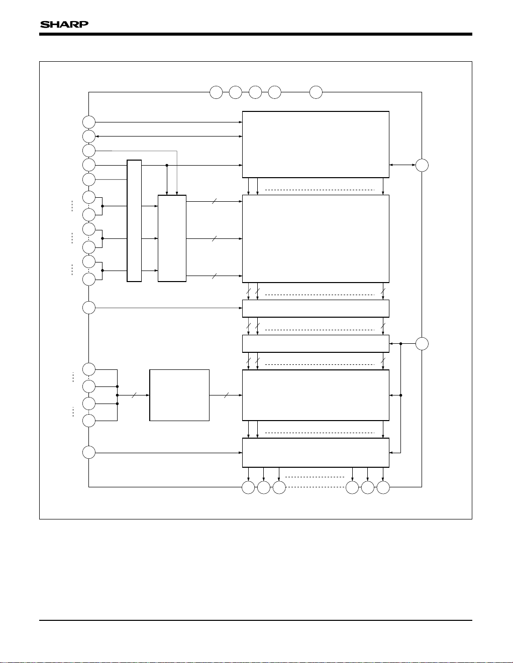
BLOCK DIAGRAM
CKN 423
POL 427
397
428
433
Y
0P
X2N
LS
X
0P
SPOI 434
LBR 400
VH0 420
VL0 401
VL64 409
VH
64 412
1
CKP 424
391
392
Z0P
Y2N
386Z2N
425
382
410
385
398399
422421
REV 426
SPIO
V
LS
XO12YO13ZO1 XO128
383
YO128
384
ZO128
6
6
6
64 x 2
18
6
6
6
6
6
6
6
6
6
12821
V
CC VCC GND GND
411
GND
SHIFT REGISTER
SAMPLING MEMORY
HOLD MEMORY
DATA
LATCH
REFERENCE
VOLTAGE
GENERATION
CIRCUIT
LEVEL SHIFTER
DA CONVERTER
OUTPUT CIRCUIT
COMPARATOR
Page 4

LH168M
4
FUNCTIONAL OPERATIONS OF EACH BLOCK
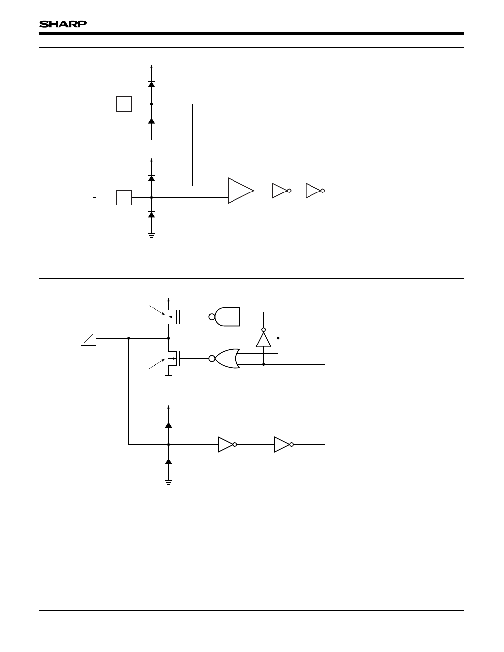
INPUT/OUTPUT CIRCUITS
I
V
CC
GND
To Internal Circuit
Fig. 1 Input Circuit (1)
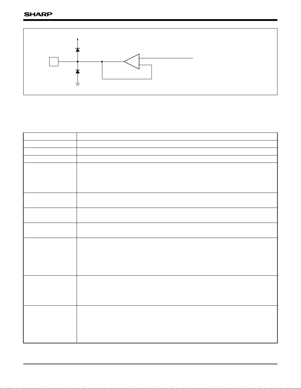
¿Applicable pins¡
LBR, LS, REV
I
V
CC
GND GND
To Internal Circuit
Fig. 2 Input Circuit (2)
¿Applicable pin¡
POL
BLOCK FUNCTION
Shift Register
Used as a bi-directional shift register which performs the shifting operation by CK and
selects bits for data sampling.
Data Latch Used to temporary latch the input data which is sent to the sampling memory.
Comparator Convert low voltage input signal into internal [CMOS level] voltage input signal.
Sampling Memory Used to sample the data to be entered by time sharing.
Hold Memory Used for latch processing of data in the sampling memory by LS input.
Level Shifter
Used to shift the data in the hold memory to the power supply level of the analog circuit
unit and sends the shifted data to DA converter.
Reference Voltage
Generation Circuit
Used to generate a gamma-connected 64 x 2-level voltage by the resistor dividing circuit.
DA Converter
Used to generate an analog signal according to the display data and sends the signal to
the output circuit.
Output Circuit
Used as a voltage follower, configured with an operational amplifier and an output buffer,
which outputs analog signals of 64 x 2 gray scales to LCD drive output pin.
Page 5
LH168M
5
Fig. 4 Input/Output Circuit
¿Applicable pins¡
SPIO, SPOI
I
**P
**N
V
CC
GND
To Internal Circuit
Comparator
Differential
Input
I
V
CC
GND
+
–
Fig. 3 Input Circuit (3)
¿Applicable pin¡
CKP, CKN, X0P-X2P,
X
0N-X2N, Y0P-Y2P,
Y
0N-Y2N, Z0P-Z2P,
Z
0N-Z2N
** : CK, X0-X2,
Y
0-Y2, Z0-Z2
VCC
GND
Nch Tr
Output Signal
Output Control Signal
VCC
GND
To Internal Circuit
I
O
Pch Tr
Page 6
LH168M
6
O
V
LS
GND
From Internal Circuit
Operational Amplifier
+
–
Fig. 5 Output Circuit
¿Applicable pins¡
XO
1-XO128,
YO
1-YO128,
ZO
1-ZO128
FUNCTIONAL DESCRIPTION
Pin Functions
SYMBOL FUNCTIONS
V
CC Used as power supply pin for digital circuit, connected to +3.0 to +3.6 V.
VLS Used as power supply pin for analog circuit, connected to +8.0 to +12.0 V.
GND Used as ground pin, connected to 0 V.
SPIO
SPOI
Used as input pins of start pulse and also used as output pins for cascade connection.
When "H" is input into start pulse input pin, data sampling is started. On completion of
sampling, "H" pulse is output to output pin for cascade connection. Pin functions are
selected by LBR. For selecting, refer to "Functional Operations".
LBR
Used as input pin for selecting the shift register direction. For selecting, refer to
"Functional Operations".
LS
Used as input pin for parallel transfer from sampling memory to hold memory. Data is
transferred at the rising edge and output from LCD drive output pin.
CKP
CKN
Used as shift clock input pin. Data is latched into sampling memory from data input pin at
the falling edge and the rising edge. (Use RSDS input voltage : 0 V to V
CC – 1.0 V)
VH
0-VH64
VL0-VL64
Used as reference voltage input pins. Hold the reference voltage fixed during the period of
LCD drive output. For relation between input data and output voltage values, refer to
"Output Voltage Value". For internal gamma correction, refer to "Gamma Correction
Value". Observe the following relation for input voltage.
V
LS > VH0 ≥ VH8 ≥ π ≥ VH64 ≥ VL64 ≥ VL56 ≥ π ≥ VL0 > GND.
X
0P-X2N
Y
0P-Y2N
Z0P-Z2N
Used as data input pins of R, G, and B colors. 3-bit data are input from data pins at the
falling edge and the rising edge of CKP (CKN). For relation between input data and output
voltage values, refer to "Functional Operations" and "Output Voltage Value". Select the
data to be entered into X, Y, and Z according to picture element arrays of the panel.
XO
1-XO128,
YO
1-YO128,
ZO
1-ZO128
Used as LCD drive output pins which output the voltage c/orresponding to the input of data
input pins (X0P to X2N, Y0P to Y2N, Z0P to Z2N). Data of XO1 to XO128 correspond to X0P
to X
2N. Data of YO1 to YO128 correspond to Y0P to Y2N, and data of ZO1 to ZO128
correspond to Z0P to Z2N. For relation between input data and output voltage values, refer
to "Functional Operations" and "Output Voltage Value".
Page 7

LH168M
7
SYMBOL FUNCTIONS
REV
Used as polarity exchange pin of LCD drive output. Data is taken at the term when LS is
"H" and the output polarity of LCD drive output pin is determined. For exchanging, refer to
"Output Characteristics".
Used as input pin for input data polarity exchange. When "L" is entered, display data
becomes normal mode. When "H" is entered, input data becomes polarity exchange mode.
For relation between input data and output voltage value, refer to "Output Voltage Value".
These pins are pulled down at the inside.
POL
Functional Operations
The following describes the relation between data
input pin and output direction.
The following describes the relation between LBR
pin, SPOI pin, SPIO pin and output direction
Data input pin
X0P-X2NY0P-Y2NZ0P-Z2N ππππππππππππππππ X0P-X2NY0P-Y2NZ0P-Z2N
Output
direction
XO
1 YO1 ZO1 ππππππππππππππππ XO128 YO128 ZO128
NOTE :
Color data corresponding to X, Y, and Z vary depending on the output direction.
PIN
OUTPUT DIRECTION
LBR H L
SPOI Input Output
SPIO Output Input
LEFT SHIFT (ZO128, YO128, XO128/ZO1, YO1, XO1)RIGHT SHIFT (XO1, YO1, ZO1/XO128, YO128, ZO128)
Page 8

LH168M
8
NOTES :
+ : The gray scale voltages corresponding to reference voltage VH0 to VH64 are outputs.
– : The gray scale voltages corresponding to reference voltage VL
0 to VL64 are outputs.
Output Characteristics
The following describes the relation between REV
pin and output polarity of LCD drive pin.
REV "H" "L"
XO
1 +–
YO1 –+
ZO
1 +–
XO2 –+
YO
2 +–
ZO
2 –+
XO3 +–
YO
3 –+
ZO3 +–
XO
4 –+
YO
4 +–
ZO4 –+
:::
XO
125 +–
YO
125 –+
ZO
125 +–
XO126 –+
YO
126 +–
ZO126 –+
XO
127 +–
YO
127 –+
ZO127 +–
XO
128 –+
YO128 +–
ZO
128 –+
Page 9

LH168M
9
X0
CKP
123
123
SPIO
(SPOI)
X
0P-X0N
X
1P-X1N
X
2P-X2N
Y
0P-Y0N
Y
1P-Y1N
Y
2P-Y2N
Z
0P-Z0N
Z
1P-Z1N
Z
2P-Z2N
X
1 X0 X1 X0 X1 X0 X1
X2 X3 X2 X3 X2 X3 X2 X3
X4 X5 X4 X5 X4 X5 X4 X5
Y0 Y1 Y0 Y1 Y0 Y1 Y0 Y1
Y2 Y3 Y2 Y3 Y2 Y3 Y2 Y3
Y4 Y5 Y4 Y5 Y4 Y5 Y4 Y5
Z0 Z1 Z0 Z1 Z0 Z1 Z0 Z1
Z2 Z3 Z2 Z3 Z2 Z3 Z2 Z3
Z4 Z5 Z4 Z5 Z4 Z5 Z4 Z5
Timing Diagram
Page 10

10
LH168M
Output Voltage Value
Two voltages are selected from all of the reference
voltages (V
0-V64) by the upper 3-bit data (D5, D4
and D3) of the 6-bit input data (D5, D4, D3, D2, D1
and D0) taken by time sharing, and intermediate
value is determined by the lower 3-bit data (D
2, D1
and D0). The Vi is a reference voltage (VHi or VLi)
that is determined by the polarity exchange input
(REV). Relation between input data and output
voltage values is shown below.
(
i = 0, 8, 16, 24, 32, 40, 48, 56, 64)
(1) Output voltage when reference voltage is VH
0 to VH64.
INPUT
DATA
OUTPUT VOLTAGE INPUT
DATA
OUTPUT VOLTAGE
POL = "L" POL = "H" POL = "L" POL = "H"
0VH0
VH64+ (VH56– VH64) x 1/8
20 VH32
VH32+ (VH24– VH32) x 1/8
1
VH8+ (VH0– VH8) x 7/8
VH64+ (VH56– VH64) x 2/8
21
VH40+ (VH32– VH40) x 7/8 VH32+ (VH24– VH32) x 2/8
2
VH8+ (VH0– VH8) x 6/8
VH64+ (VH56– VH64) x 3/8
22
VH40+ (VH32– VH40) x 6/8 VH32+ (VH24– VH32) x 3/8
3
VH8+ (VH0– VH8) x 5/8
VH64+ (VH56– VH64) x 4/8
23
VH40+ (VH32– VH40) x 5/8 VH32+ (VH24– VH32) x 4/8
4
VH8+ (VH0– VH8) x 4/8
VH64+ (VH56– VH64) x 5/8
24
VH40+ (VH32– VH40) x 4/8 VH32+ (VH24– VH32) x 5/8
5
VH8+ (VH0– VH8) x 3/8
VH64+ (VH56– VH64) x 6/8
25
VH40+ (VH32– VH40) x 3/8 VH32+ (VH24– VH32) x 6/8
6
VH8+ (VH0– VH8) x 2/8
VH64+ (VH56– VH64) x 7/8
26
VH40+ (VH32– VH40) x 2/8 VH32+ (VH24– VH32) x 7/8
7
VH8+ (VH0– VH8) x 1/8
VH56 27
VH40+ (VH32– VH40) x 1/8
VH24
8VH8
VH56+ (VH48– VH56) x 1/8
28 VH40
VH24+ (VH16– VH24) x 1/8
9
VH16+ (VH8– VH16) x 7/8 VH56+ (VH48– VH56) x 2/8
29
VH48+ (VH40– VH48) x 7/8 VH24+ (VH16– VH24) x 2/8
A
VH16+ (VH8– VH16) x 6/8 VH56+ (VH48– VH56) x 3/8
2A
VH48+ (VH40– VH48) x 6/8 VH24+ (VH16– VH24) x 3/8
B
VH16+ (VH8– VH16) x 5/8 VH56+ (VH48– VH56) x 4/8
2B
VH48+ (VH40– VH48) x 5/8 VH24+ (VH16– VH24) x 4/8
C
VH16+ (VH8– VH16) x 4/8 VH56+ (VH48– VH56) x 5/8
2C
VH48+ (VH40– VH48) x 4/8 VH24+ (VH16– VH24) x 5/8
D
VH16+ (VH8– VH16) x 3/8 VH56+ (VH48– VH56) x 6/8
2D
VH48+ (VH40– VH48) x 3/8 VH24+ (VH16– VH24) x 6/8
E
VH16+ (VH8– VH16) x 2/8 VH56+ (VH48– VH56) x 7/8
2E
VH48+ (VH40– VH48) x 2/8 VH24+ (VH16– VH24) x 7/8
F
VH16+ (VH8– VH16) x 1/8
VH48 2F
VH48+ (VH40– VH48) x 1/8
VH16
10 VH16
VH48+ (VH40– VH48) x 1/8
30 VH48
VH16+ (VH8– VH16) x 1/8
11
VH24+ (VH16– VH24) x 7/8 VH48+ (VH40– VH48) x 2/8
31
VH56+ (VH48– VH56) x 7/8 VH16+ (VH8– VH16) x 2/8
12
VH24+ (VH16– VH24) x 6/8 VH48+ (VH40– VH48) x 3/8
32
VH56+ (VH48– VH56) x 6/8 VH16+ (VH8– VH16) x 3/8
13
VH24+ (VH16– VH24) x 5/8 VH48+ (VH40– VH48) x 4/8
33
VH56+ (VH48– VH56) x 5/8 VH16+ (VH8– VH16) x 4/8
14
VH24+ (VH16– VH24) x 4/8 VH48+ (VH40– VH48) x 5/8
34
VH56+ (VH48– VH56) x 4/8 VH16+ (VH8– VH16) x 5/8
15
VH24+ (VH16– VH24) x 3/8 VH48+ (VH40– VH48) x 6/8
35
VH56+ (VH48– VH56) x 3/8 VH16+ (VH8– VH16) x 6/8
16
VH24+ (VH16– VH24) x 2/8 VH48+ (VH40– VH48) x 7/8
36
VH56+ (VH48– VH56) x 2/8 VH16+ (VH8– VH16) x 7/8
17
VH24+ (VH16– VH24) x 1/8
VH40 37
VH56+ (VH48– VH56) x 1/8
VH8
18 VH24
VH40+ (VH32– VH40) x 1/8
38 VH56
VH8+ (VH0– VH8) x 1/8
19
VH32+ (VH24– VH32) x 7/8 VH40+ (VH32– VH40) x 2/8
39
VH64+ (VH56– VH64) x 7/8
VH8+ (VH0– VH8) x 2/8
1A
VH32+ (VH24– VH32) x 6/8 VH40+ (VH32– VH40) x 3/8
3A
VH64+ (VH56– VH64) x 6/8
VH8+ (VH0– VH8) x 3/8
1B
VH32+ (VH24– VH32) x 5/8 VH40+ (VH32– VH40) x 4/8
3B
VH64+ (VH56– VH64) x 5/8
VH8+ (VH0– VH8) x 4/8
1C
VH32+ (VH24– VH32) x 4/8 VH40+ (VH32– VH40) x 5/8
3C
VH64+ (VH56– VH64) x 4/8
VH8+ (VH0– VH8) x 5/8
1D
VH32+ (VH24– VH32) x 3/8 VH40+ (VH32– VH40) x 6/8
3D
VH64+ (VH56– VH64) x 3/8
VH8+ (VH0– VH8) x 6/8
1E
VH32+ (VH24– VH32) x 2/8 VH40+ (VH32– VH40) x 7/8
3E
VH64+ (VH56– VH64) x 2/8
VH8+ (VH0– VH8) x 7/8
1F
VH32+ (VH24– VH32) x 1/8
VH32 3F
VH64+ (VH56– VH64) x 1/8
VH0
Page 11

11
LH168M
(2) Output voltage when reference voltage is VL0 to VL64.
INPUT
DATA
OUTPUT VOLTAGE INPUT
DATA
OUTPUT VOLTAGE
POL = "L" POL = "H" POL = "L" POL = "H"
0VL0
VL64+ (VL56– VL64) x 1/8
20 VL32
VL32+ (VL24– VL32) x 1/8
1
VL8+ (VL0– VL8) x 7/8
VL64+ (VL56– VL64) x 2/8
21
VL40+ (VL32– VL40) x 7/8 VL32+ (VL24– VL32) x 2/8
2
VL8+ (VL0– VL8) x 6/8
VL64+ (VL56– VL64) x 3/8
22
VL40+ (VL32– VL40) x 6/8 VL32+ (VL24– VL32) x 3/8
3
VL8+ (VL0– VL8) x 5/8
VL64+ (VL56– VL64) x 4/8
23
VL40+ (VL32– VL40) x 5/8 VL32+ (VL24– VL32) x 4/8
4
VL8+ (VL0– VL8) x 4/8
VL64+ (VL56– VL64) x 5/8
24
VL40+ (VL32– VL40) x 4/8 VL32+ (VL24– VL32) x 5/8
5
VL8+ (VL0– VL8) x 3/8
VL64+ (VL56– VL64) x 6/8
25
VL40+ (VL32– VL40) x 3/8 VL32+ (VL24– VL32) x 6/8
6
VL8+ (VL0– VL8) x 2/8
VL64+ (VL56– VL64) x 7/8
26
VL40+ (VL32– VL40) x 2/8 VL32+ (VL24– VL32) x 7/8
7
VL8+ (VL0– VL8) x 1/8
VL56 27
VL40+ (VL32– VL40) x 1/8
VL24
8VL8
VL56+ (VL48– VL56) x 1/8
28 VL40
VL24+ (VL16– VL24) x 1/8
9
VL16+ (VL8– VL16) x 7/8 VL56+ (VL48– VL56) x 2/8
29
VL48+ (VL40– VL48) x 7/8 VL24+ (VL16– VL24) x 2/8
A
VL16+ (VL8– VL16) x 6/8 VL56+ (VL48– VL56) x 3/8
2A
VL48+ (VL40– VL48) x 6/8 VL24+ (VL16– VL24) x 3/8
B
VL16+ (VL8– VL16) x 5/8 VL56+ (VL48– VL56) x 4/8
2B
VL48+ (VL40– VL48) x 5/8 VL24+ (VL16– VL24) x 4/8
C
VL16+ (VL8– VL16) x 4/8 VL56+ (VL48– VL56) x 5/8
2C
VL48+ (VL40– VL48) x 4/8 VL24+ (VL16– VL24) x 5/8
D
VL16+ (VL8– VL16) x 3/8 VL56+ (VL48– VL56) x 6/8
2D
VL48+ (VL40– VL48) x 3/8 VL24+ (VL16– VL24) x 6/8
E
VL16+ (VL8– VL16) x 2/8 VL56+ (VL48– VL56) x 7/8
2E
VL48+ (VL40– VL48) x 2/8 VL24+ (VL16– VL24) x 7/8
F
VL16+ (VL8– VL16) x 1/8
VL48 2F
VL48+ (VL40– VL48) x 1/8
VL16
10 VL16
VL48+ (VL40– VL48) x 1/8
30 VL48
VL16+ (VL8– VL16) x 1/8
11
VL24+ (VL16– VL24) x 7/8 VL48+ (VL40– VL48) x 2/8
31
VL56+ (VL48– VL56) x 7/8 VL16+ (VL8– VL16) x 2/8
12
VL24+ (VL16– VL24) x 6/8 VL48+ (VL40– VL48) x 3/8
32
VL56+ (VL48– VL56) x 6/8 VL16+ (VL8– VL16) x 3/8
13
VL24+ (VL16– VL24) x 5/8 VL48+ (VL40– VL48) x 4/8
33
VL56+ (VL48– VL56) x 5/8 VL16+ (VL8– VL16) x 4/8
14
VL24+ (VL16– VL24) x 4/8 VL48+ (VL40– VL48) x 5/8
34
VL56+ (VL48– VL56) x 4/8 VL16+ (VL8– VL16) x 5/8
15
VL24+ (VL16– VL24) x 3/8 VL48+ (VL40– VL48) x 6/8
35
VL56+ (VL48– VL56) x 3/8 VL16+ (VL8– VL16) x 6/8
16
VL24+ (VL16– VL24) x 2/8 VL48+ (VL40– VL48) x 7/8
36
VL56+ (VL48– VL56) x 2/8 VL16+ (VL8– VL16) x 7/8
17
VL24+ (VL16– VL24) x 1/8
VL40 37
VL56+ (VL48– VL56) x 1/8
VL8
18 VL24
VL40+ (VL32– VL40) x 1/8
38 VL56
VL8+ (VL0– VL8) x 1/8
19
VL32+ (VL24– VL32) x 7/8 VL40+ (VL32– VL40) x 2/8
39
VL64+ (VL56– VL64) x 7/8
VL8+ (VL0– VL8) x 2/8
1A
VL32+ (VL24– VL32) x 6/8 VL40+ (VL32– VL40) x 3/8
3A
VL64+ (VL56– VL64) x 6/8
VL8+ (VL0– VL8) x 3/8
1B
VL32+ (VL24– VL32) x 5/8 VL40+ (VL32– VL40) x 4/8
3B
VL64+ (VL56– VL64) x 5/8
VL8+ (VL0– VL8) x 4/8
1C
VL32+ (VL24– VL32) x 4/8 VL40+ (VL32– VL40) x 5/8
3C
VL64+ (VL56– VL64) x 4/8
VL8+ (VL0– VL8) x 5/8
1D
VL32+ (VL24– VL32) x 3/8 VL40+ (VL32– VL40) x 6/8
3D
VL64+ (VL56– VL64) x 3/8
VL8+ (VL0– VL8) x 6/8
1E
VL32+ (VL24– VL32) x 2/8 VL40+ (VL32– VL40) x 7/8
3E
VL64+ (VL56– VL64) x 2/8
VL8+ (VL0– VL8) x 7/8
1F
VL32+ (VL24– VL32) x 1/8
VL32 3F
VL64+ (VL56– VL64) x 1/8
VL0
Page 12

12
LH168M
External Reference Voltage
LH168M
VH
0
VH8
VH16
VH24
VH32
VH40
VH48
VH56
VH64
VL64
VL56
VL48
VL40
VL32
VL24
VL16
VL8
VL0
R0
R1
R2
R3
R4
R5
R6
R8
R9
R10
R11
R12
R13
R14
R15
R7
8 equal parts
8 equal parts
8 equal parts
8 equal parts
8 equal parts
8 equal parts
8 equal parts
8 equal parts
8 equal parts
8 equal parts
8 equal parts
8 equal parts
8 equal parts
8 equal parts
8 equal parts
8 equal parts
R0 1.00
R
1 0.50
R2 0.50
R
3 0.50
R4 0.50
R
5 0.50
R
6 0.50
R7 1.00
R
8 1.00
R
9 0.50
R10 0.50
R
11 0.50
R12 0.50
R
13 0.50
R
14 0.50
R15 1.00
The following shows the ratio of ‹ correction resistance, when R0 equals 1.
‹ (Gamma) Correction Value
Between reference voltage input pins VH0 and
VH
64, 64 resistors are connected in series.
And between reference voltage input pins VL
0 and
VL
64, 64 resistors are connected in series. No
resistor is connected between reference voltage
input pins VH
64 and VL64.
The ‹ correction curve is a broken line connected
between intermediate voltage inputs (VH
8, VH16,
VH
24, VH32, VH40, VH48, VH56, VL8, VL16, VL24,
VL
32, VL40, VL48 and VL56). Each ‹ correction
value between the intermediate voltage inputs is
divided into 8 parts by the same resistor.
Page 13

13
LH168M
ABSOLUTE MAXIMUM RATINGS
PARAMETER SYMBOL APPLICABLE PINS RATING UNIT NOTE
Supply voltage
V
CC VCC –0.3 to +6.0 V
1, 2
V
LS VLS –0.3 to +13.0 V
Input voltage
V
I VH0-VL0 –0.3 to VLS + 0.3 V
Storage temperature T
STG –45 to +125 ˚C
V
I
SPIO, SPOI, CKP, CKN, LS,
REV, LBR, POL, X
0P-X2N,
Y
0P-Y2N, Z0P-Z2N
–0.3 to V
CC + 0.3 V
V–0.3 to V
LS + 0.3
XO1-ZO
128
VO
V–0.3 to VCC + 0.3SPIO, SPOIVO
Output voltage
RECOMMENDED OPERATING CONDITIONS
NOTES :
1. TA = +25 ˚C
2. The maximum applicable voltage on any pin with respect to GND (0 V).
NOTE :
1. The applicable voltage on any pin with respect to GND (0 V).
PARAMETER SYMBOL MAX. UNIT NOTE
Supply voltage
V
CC
1
Reference voltage input
VH
0-VH64
VLS – 0.1
V
Clock frequency f
CK 68 MHz
MIN. TYP.
+3.0
0.5V
LS
VLS
+3.6 V
+8.0 +12.0 V
–20 ˚C+75T
OPROperating temperature
pF150C
L
LCD drive output load capacity
VL0-VL64 +0.1 0.5VLS V
PRECAUTIONS
Precautions when connecting or disconnecting
the power supply
This IC has some power supply pins, so it may be
permanently damaged by a high current which may
flow if voltage is supplied to the LCD drive power
supply while the logic system power supply is
floating. Therefore, when connecting the power
supply, observe the following sequence.
V
CC / logic input / VLS, VH0-VH64, VL0-VL64
When disconnecting the power supply, follow the
reverse sequence.
Reference voltage input
The relation of the reference voltage input is shown
here.
V
LS > VH0 ≥ VH8 ≥ π ≥ VH56 ≥ VH64 ≥ 0.5VLS ≥
VL
64 ≥ VL56 ≥ π ≥ VL8 ≥ VL0 > GND
Maximum ratings
When connecting or disconnecting the power
supply, this IC must be used within the range of the
absolute maximum ratings.
Target output load
This IC is designed for a 150 pF output load
capacity. When using this IC for other than 150 pF
panels, confirm the device is having no problem
before using it.
Page 14

LH168M
14
PARAMETER
SYMBOL
CONDITIONS APPLICABLE PINS MIN. TYP. MAX. UNIT NOTE
Input "Low" voltage V
IL SPIO, SPOI, LS, LBR,
REV, POL
GND 0.3VCC V
Input "High" voltage V
IH 0.7VCC VCC V
RSDS Input "Low"
voltage
V
ILRSDS
X0P-X2N, Y0P-Y2N,
Z
0P-Z2N, CKP, CKN
–200 mV
1
RSDS Input "High"
voltage
V
IHRSDS 200 mV
RSDS reference
voltage
VCOMRSDS
GND + 0.1
1.2
VCC – 1.2
V2
Output "Low" voltage V
OL IOL = 0.3 mA
SPIO, SPOI
GND
GND + 0.4
V
Output "High" voltage VOH IOH = –0.3 mA
VCC – 0.4
VCC V
Input "Low" current I
ILL1
X0P-X2N, Y0P-Y2N, Z0P-Z2N,
SPIO, SPOI, CKP, CKN, LS
LBR, REV, POL
10 µA
Input "High" current
I
ILH1
X0P-X2N, Y0P-Y2N,
Z0P-Z2N, SPIO, SPOI,
CKP, CKN, LS, LBR
10 µA
I
ILH2 POL 400 µA
Supply current
(In operation mode)
I
CC1
fCK = 65 MHz
f
LS = 50 kHz
fREV = 50 kHz
(Data sampling state)
VCC-GND
14 mA
Supply current
(In standby mode)
I
CC2
fCK = 65 MHz
fLS = 50 kHz
SPI = REV = GND is fixed.
(Standby state)
2mA
Supply current
(In operation mode)
I
LS1
fCK = 65 MHz
fLS = 50 kHz
f
REV = 50 kHz
(Data sampling state)
VLS-GND
5mA
Supply current
(In standby mode)
I
LS2
fCK = 65 MHz
f
LS = 50 kHz
SPI = REV = GND is fixed.
(Standby state)
4mA
Output voltage range V
OUT
XO1-ZO128
GND + 0.2
VLS – 0.2
V
3Deviations between
output voltage pins
V
OD –20 +20 mV
Output current I
O1-IO4 100 200 µA 4
Resistance between
reference voltage input pins
RGMAH VH0-VH64 10 20 30 k$
R
GMAL VL0-VL64 10 20 30 k$
ELECTRICAL CHARACTERISTICS
DC Characteristics
(VCC = +3.0 to +3.6 V, VLS = +8.0 to +12.0 V, TOPR = –20 to +75 ˚C)
Page 15

15
LH168M
NOTES :
1. VCOMRSDS = (V**P+V**N)/2 = 1.2 V
**P = X
0P-X2P, Y0P-Y2P, Z0P-Z2P
**N = X
0N-X2N, Y0N-Y2N, Z0N-Z2N
2. V
DIFFRSDS = V**P – V**N = 0.2 V
3. Criterion of evaluating voltage deviations.
(a) Between output voltage pins
Measuring values : Output voltage value at the time after
10 µs at the rising edge of LS.
(Average of several times)
(Conditions) Output load capacity is 150 pF.
In a state when the reference voltage is fixed.
Expecting values : Calculated following these specifications.
(Conditions) In a state when the reference voltage is fixed.
(b) Between LCD drivers.
Measuring values : Applicable to (a).
(Conditions) Applicable to (a).
Expecting values : Applicable to (a).
(Conditions) Applicable to (a).
Each input voltage between the LCD drivers must be
made perfectly equal by connecting corresponding
reference voltage input pins.
4. Io
1 : Applied voltage = 8.0 V for output pins XO1 to ZO128.
Output voltage = 7.5 V for output pins XO
1 to ZO128.
V
LS = 10.0 V
Io
2 : Applied voltage = 7.0 V for output pins XO1 to ZO128.
Output voltage = 7.5 V for output pins XO
1 to ZO128.
V
LS = 10.0 V
Io
3 : Applied voltage = 3.0 V for output pins XO1 to ZO128.
Output voltage = 2.5 V for output pins XO
1 to ZO128.
V
LS = 10.0 V
Io
4 : Applied voltage = 2.0 V for output pins XO1 to ZO128.
Output voltage = 2.5 V for output pins XO
1 to ZO128.
V
LS = 10.0 V
Page 16

16
LH168M
AC Characteristics (VCC = +3.0 to +3.6 V, VLS = +8.0 to +12.0 V, TOPR = –20 to +75 ˚C)
PARAMETER
SYMBOL
CONDITIONS APPLICABLE PINS MIN. TYP. MAX. UNIT
Clock frequency f
CK
CKP
68 MHz
"H" level pulse width tCWH 6ns
Input rise time t
CR 5ns
Input fall time tCF 5ns
Data setup time t
SUD X0P-X2N, Y0P-Y2N,
Z0P-Z2N
3ns
Data hold time tHD 0ns
Start pulse setup time t
SUSP 1ns
Start pulse hold time t
HSP 2ns
Start pulse output
delay time
t
DSP CL = 15 pF 13 ns
LCD drive output
delay time 1
t
DO1 3µs
LCD drive output
delay time 2
t
DO2 10 µs
SPIO, SPOI
ns6tCWL"L" level pulse width
ns
1
-------f
CK
tWSPStart pulse width
ns7t
HLS
LS signal-CK signal
hold time
ns
1
-------fCK
tLSSP
LS signal-SPI signal
setup time
C
L = 150 pF
C
L = 150 pF
XO
1-ZO128
LS
LS signal "H" level
width
t
WLS
1
-------f
CK
ns
ns10t
HRV
REV signal-LS signal
hold time
ns14t
SURV
REV signal-LS signal
setup time
REV
Page 17

17
LH168M
tCF
tHSP
tCWH tCWL
tSUSP
tWSP
tCR
1
f
CK
tSUD
tDSP
tHLS tWLS
tLSSP
tHRVtSURV
tDO1
tDO2
tSUD
tHD tHD
LAST – 2 LAST – 1
Target voltage ±(V
LS x 0.1)
Target voltage (6-bit accuracy)
CKP
(RSDS)
CKP
(RSDS)
SPIO Input
(SPOI)
SPIO Output
(SPOI)
SPIO Input
(SPOI)
XO
1-ZO128
LS
REV
**P – **N (RSDS)
**P = X
0P-X2P, Y0P-Y2P, Z0P-Z2P
**N = X
0N-X2N, Y0N-Y2N, Z0N-Z2N
12
Timing Chart
 Loading...