

Page 1
In the absence of confirmation by device specification sheets, SHARP takes no responsibility for any defects that may occur in equipment using any SHARP devices shown in
catalogs, data books, etc. Contact SHARP in order to obtain the latest device specification sheets before using any SHARP device.
1
DESCRIPTION
The LH168K is a 324-output TFT-LCD source
driver IC which can simultaneously display 262 144
colors in 64 gray scales.
FEATURES
• Selectable number of LCD drive outputs :
324/321/312/309
• Built-in 6-bit digital input DAC
• Dot-inversion drive : Outputs the inverted gray
scale voltages between LCD drive pins next to
each other
• 2-port input for each circuit of data inputs R, G
and B, and it is possible to sample and hold
display data of two pixels at the same time at
324-output and 312-output modes. 1-port input for
each circuit of data inputs R, G and B at 321output and 309-output modes.
• Possible to display 262 144 colors in 64 gray scales
with reference voltage input of 18 gray scales : This
reference voltage input corresponds to ‹ correction
and intermediate reference voltage input can be
abbreviated
• Cascade connection
• Sampling sequence :
Output shift direction can be selected
XO
1, YO1, ZO1/XO108, YO108, ZO108 or
ZO
108, YO108, XO108/ZO1, YO1, XO1
• Shift clock frequency : 55 MHz (MAX.)
• Supply voltages
–V
CC (for logic system) : +2.7 to +3.6 V
–V
LS (for LCD drive system) : +12 V (MAX.)
• Package : 395-pin TCP (Tape Carrier Package)
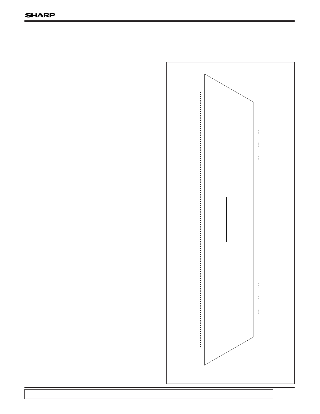
PIN CONNECTIONS
LH168K
LH168K
324-output TFT-LCD Source Driver IC
XO108
YO108
ZO108
322
323
324
XO
1
YO1
ZO1
1
2
3
CHIP SURFACE
GND
VLS
GND
MODE
PBS
XB5
XB0
XA5
XA0
YA5
YA0
SPOI
VH0
VH8
VH16
VH24
VH32
VH40
VH48
VH56
VH63
VL63
VL56
VL48
VL40
VL32
VL24
VL16
VL8
VL0
POLB
POLA
CK
SPIO
LS
REV2
REV
YB5
YB0
ZB5
ZB0
ZA5
ZA0
LBR
VCC
VLS
GND
395
394
393
392
391
390
385
384
379
378
373
372
371
370
369
368
367
366
365
364
363
362
361
360
359
358
357
356
355
354
353
352
351
350
349
348
347
346
341
340
335
334
329
328
327
326
325
395-PIN TCP
TOP VIEW
NOTE :
Doesn't prescribe TCP outline.
Page 2
LH168K
2
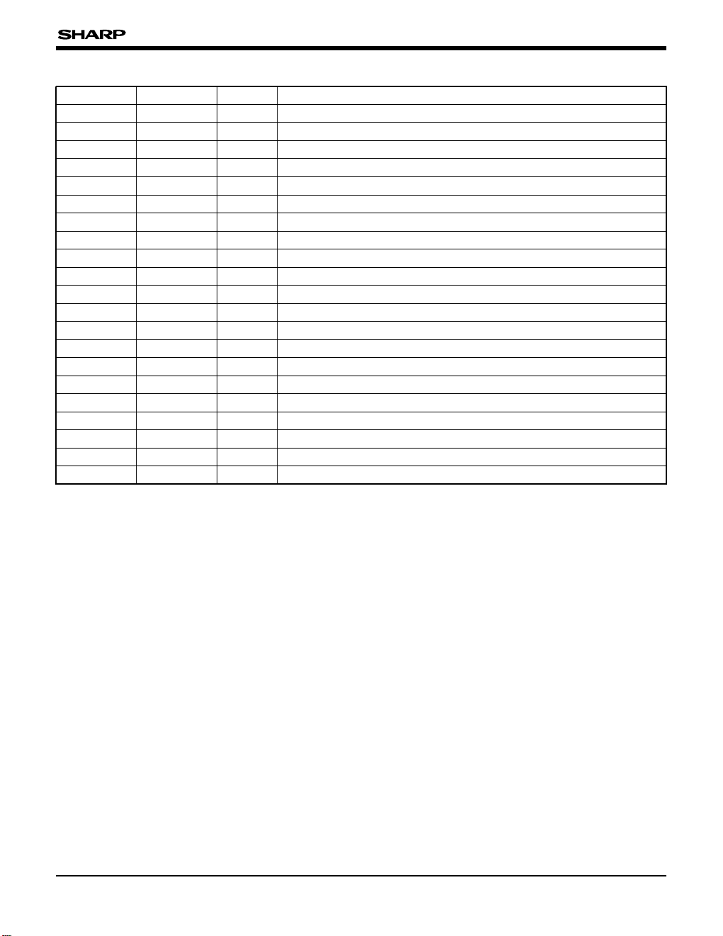
PIN DESCRIPTION
PIN NO. SYMBOL I/O DESCRIPTION
1 to 324 XO
1-ZO108 O LCD drive output pins
325, 393, 395 GND – Ground pins
326, 394 V
LS – Power supply pins for analog circuit
327 V
CC – Power supply pin for digital circuit
328 LBR I Shift direction selection input pin
329 to 334 ZA
0-ZA5 I Data input pins
335 to 340 ZB0-ZB5 I Data input pins
341 to 346 YB
0-YB5 I Data input pins
347, 348 REV, REV
2 I LCD drive output polarity exchange input pins
349 LS I Latch input pin
350 SPIO I/O Start pulse input/cascade output pin
351 CK I Shift clock input pin
352, 353 POLA, POLB I Input data polarity exchange input pins
354 to 362 VL
0-VL63 I Reference voltage input pins
363 to 371 VH63-VH0 I Reference voltage input pins
Data input pinsIXB
0-XB5385 to 390
Data input pinsIXA
0-XA5379 to 384
Data input pinsIYA
0-YA5373 to 378
Start pulse input/cascade output pinI/OSPOI372
392 MODE I Input pin for selecting the number of LCD drive outputs
391 PBS I 2-port/1-port selection input pin
Page 3
LH168K
3
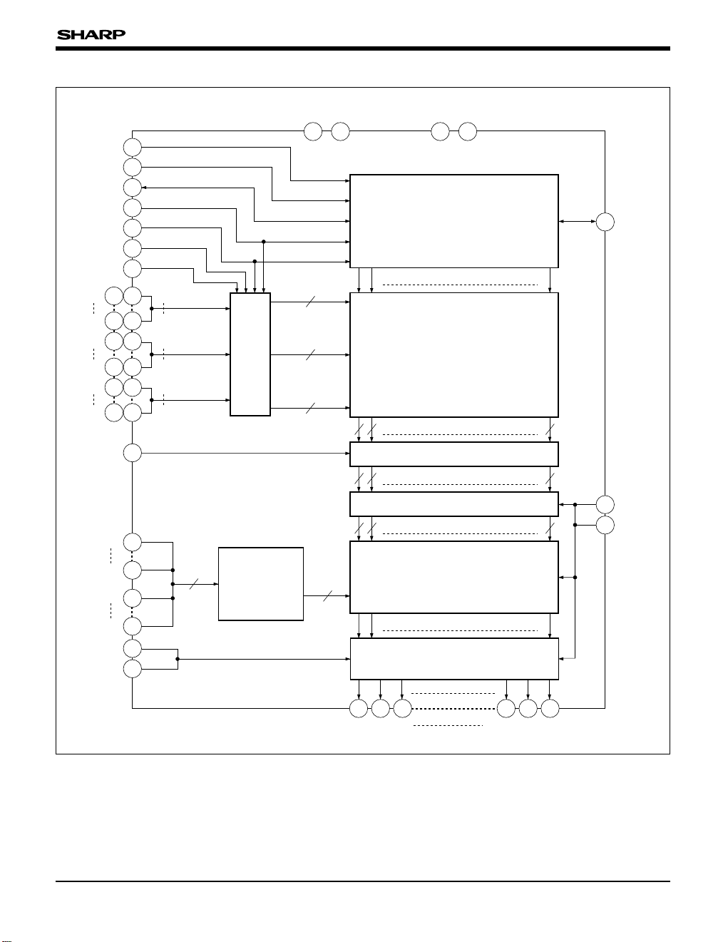
BLOCK DIAGRAM
CK 351
PBS 391
341
390
385
YA0 373
XA5
LS
384
XA0 XB0
XB5
YB0
YB5
ZB0
ZB5
379
SPOI 372
PLOB 353
POLA 352
LBR 328
MODE 392
VH0 371
VH
63
VL63
REV 347
REV2 348
VL0 354
1
335
346
ZA0 329
YA5 378
340ZA5 334
349
322
326
350
393327
SPIO
V
LS
394
VLS
XO12YO13ZO1 XO108
323
YO108
324
ZO108
6 x 2
6 x 2
6 x 2
6
6
6
64 x 2
18
6
6
6
6
10821
6
6
V
CC GND
395325
GND GND
SHIFT REGISTER
SAMPLING MEMORY
HOLD MEMORY
DATA
LATCH
REFERENCE
VOLTAGE
GENERATION
CIRCUIT
LEVEL SHIFTER
DA CONVERTER
OUTPUT CIRCUIT
363
362
Page 4
LH168K
4
FUNCTIONAL OPERATIONS OF EACH BLOCK
BLOCK FUNCTION
Shift Register
Used as a bi-directional shift register which performs the shifting operation by CK and
selects bits for data sampling.
Data Latch Used to temporary latch the input data which is sent to the sampling memory.
Sampling Memory Used to sample the data to be entered by time sharing.
Hold memory Used for latch processing of data in the sampling memory by LS input.
Level Shifter
Used to shift the data in the hold memory to the power supply level of the analog circuit
unit and sends the shifted data to DA converter.
Reference Voltage
Generation Circuit
Used to generate a gamma-corrected 64 x 2-level voltage by the resistor dividing circuit.
DA Converter
Used to generate an analog signal according to the display data and sends the signal to
the output circuit.
Output Circuit
Used as a voltage follower, configured with an operational amplifier and an output buffer,
which outputs analog signals of 64 x 2 gray scales to LCD drive output pin.
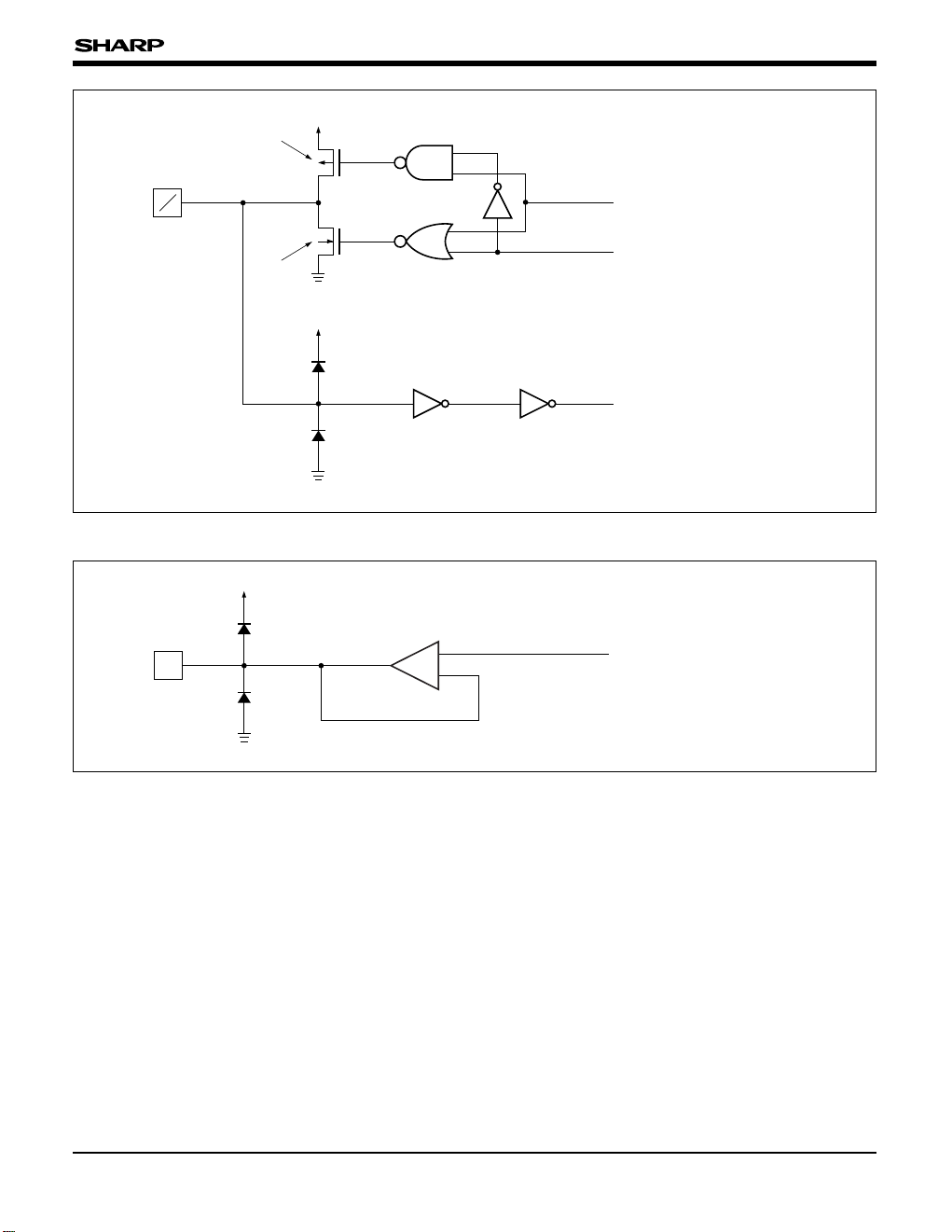
INPUT/OUTPUT CIRCUITS
I
V
CC
GND
To Internal Circuit
Fig. 1 Input Circuit (1)
¿Applicable pins¡
CK, LS, REV, LBR,
MODE, PBS,
XA
0-XA5, XB0-XB5,
YA
0-YA5, YB0-YB5,
ZA
0-ZA5, ZB0-ZB5
I
V
CC
GND
To Internal Circuit
GND
Fig. 2 Input Circuit (2)
¿Applicable pins¡
POLA, POLB, REV
2
Page 5
LH168K
5
O
V
LS
GND
From Internal Circuit
Operational Amplifier
+
–
Fig. 4 Output Circuit
¿Applicable pins¡
XO
1-XO108,
YO
1-YO108,
ZO
1-ZO108
VCC
GND
Nch Tr
Output Signal
Output Control Signal
VCC
GND
To Internal Circuit
I
O
Pch Tr
Fig. 3 Input/Output Circuit
¿Applicable pins¡
SPIO, SPOI
Page 6

LH168K
6
FUNCTIONAL DESCRIPTION
Pin Functions
SYMBOL FUNCTION
V
CC Used as power supply pin for digital circuit, connected to +2.7 to +3.6 V.
V
LS Used as power supply pin for analog circuit, connected to +8.0 to +12.0 V.
GND Used as ground pin, connected to 0 V.
SPIO
SPOI
Used as input pins of start pulse and also used as output pins for cascade connection.
When "H" is input into start pulse input pin, data sampling is started. On completion of
sampling, "H" pulse is output to output pin for cascade connection. Pin functions are
selected by LBR. For selecting, refer to "Functional Operations".
LBR
Used as input pin for selecting the shift register direction. For selecting, refer to
"Functional Operations".
LS
Used as input pin for parallel transfer from sampling memory to hold memory. Data is
transferred at the rising edge and output from LCD drive output pin.
CK
Used as shift clock input pin. Data is latched into sampling memory from data input pin at
the rising edge.
VH
0-VH63
VL0-VL63
Used as reference voltage input pins. Hold the reference voltage fixed during the period of
LCD drive output. For relation between input data and output voltage values, refer to
"Output Voltage Value". For internal gamma correction, refer to "Gamma Correction
Value". Observe the following relation for input voltage.
V
LS > VH0 ≥ VH8 ≥ π ≥ VH63 ≥ VL63 ≥ VL56 ≥ π ≥ VL0 > GND.
XA
0-XA5
YA0-YA5
ZA0-ZA5
XB0-XB5
YB0-YB5
ZB0-ZB5
Used as data input pins of R, G, and B colors. 6-bit data are input from data pins at the
rising edge of CK. When PBS is "L", 2-pixel data are input from XA0 to XA5, YA0 to YA5,
ZA
0 to ZA5 and XB0 to XB5, YB0 to YB5, ZB0 to ZB5 at the same time.
When PBS is "H", 1-pixel data is input from XA
0 to XA5, YA0 to YA5 and ZA0 to ZA5, and
fixed XB0 to XB5, YB0 to YB5 and ZB0 to ZB5 to "L" or "H". For relation between input data
and output voltage values, refer to "Functional Operations" and "Output Voltage Value".
Select the data to be entered into X, Y, and Z according to picture element arrays of the
panel.
MODE
Used as input pin for selecting the number of LCD drive outputs, which sets up operation
mode with PBS pin. When "L" is entered, it becomes 324-output/2-port input mode at PBS
pin "L" or 321-output/1-port input mode at PBS pin "H". When "H" is entered, it becomes
312-output/2-port input mode at PBS pin "L" or 309-output/1-port mode at PBS pin "H". For
selecting the number of LCD drive outputs, refer to "Output Characteristics".
PBS
Used as 2-port/1-port exchange input pin to take in data. When "L" is entered, it becomes
2-port input mode and 2-pixel data are input at the same time. When "H" is entered, it
becomes 1-port input mode.
Page 7

LH168K
7
SYMBOL FUNCTIONS
XO
1-XO108
YO1-YO108
ZO1-ZO108
Used as LCD drive output pins which output the voltage corresponding to the input of data
input pins. When 321-output mode, 3 outputs (XO
54 to ZO54) are invalid. When 312-output
mode, 12 outputs (XO
55 to XO58, YO55 to YO58, ZO55 to ZO58) are invalid. When 309-
outputs mode, 15 outputs (XO54 to XO58, YO54 to YO58, ZO54 to ZO58) are invalid. Invalid
output pins must be opened. Data of XO
1 to XO108 correspond to XA0 to XA5 and XB0 to
XB5. Data of YO1 to YO108 correspond to YA0 to YA5 and YB0 to YB5, and data of ZO0 to
ZO
108 correspond to ZA0 to ZA5 and ZB0 to ZB5. For relation between input data and
output voltage values, refer to "Functional Operations" and "Output Voltage Value".
POLA
POLB
Used as input pins for input data polarity exchange, POLA corresponds to XA
0 to XA5, YA0
to YA5 and ZA0 to ZA5, and POLB corresponds to XB0 to XB5, YB0 to YB5 and ZB0 to ZB5.
When "L" is entered, display data becomes normal mode. When "H" is entered, input data
becomes polarity exchange mode. For relation between input data and output voltage
values, refer to "Output Voltage Value". These pins are pulled down at the inside.
REV
REV
2
Used as polarity exchange pins of LCD drive output. Data is taken at the term when LS is
"H" and the output polarity of the LCD drive output pin is determined. Function of REV is
the same as function of REV
2. Input polarity exchange signal to REV, and REV2 is fixed to
"L" or opened in general.
When 321-output/309-output mode, it is possible to exchange output polarity between LCD
driver next to each other by fixing REV
2 to "L" or "H" according to position on panel. For
exchanging, refer to "Output Characteristics". REV
2 pin is pulled down at the inside.
Page 8

LH168K
8
Functional Operations
The following describes the relation between data
input pin and output direction.
(1) PBS = "L"
The following describes the relation between LBR
pin, SPOI pin, SPIO pin and output direction.
Data input pin
XA0-XA5 YA0-YA5 ZA0-ZA5 XB0-XB5 YB0-YB5 ZB0-ZB5 πππ XB0-XB5 YB0-YB5 ZB0-ZB5
Output
direction
XO
1 YO1 ZO1 XO2 YO2 ZO2 πππ XO108 YO108 ZO108
Data input pin
(2) PBS = "H"
XA0-XA5 YA0-YA5 ZA0-ZA5 XA0-XA5 YA0-YA5 ZA0-ZA5 πππ XA0-XA5 YA0-YA5 ZA0-ZA5
Output
direction
XO
1 YO1 ZO1 XO2 YO2 ZO2 πππ XO108 YO108 ZO108
PIN
OUTPUT DIRECTION
LBR H L
SPOI Input Output
SPIO Output Input
NOTE :
Color data corresponding to X, Y, and Z vary depending on the output direction.
LEFT SHIFT (ZO108, YO108, XO108/ZO1, YO1, XO1)RIGHT SHIFT (XO1, YO1, ZO1/XO108, YO108, ZO108)
Page 9

LH168K
9
YO55 + – NA NA – + NA NA
ZO
55 – + NA NA + – NA NA
XO
56 + – NA NA – + NA NA
YO
56 – + NA NA + – NA NA
ZO
56 + – NA NA – + NA NA
XO
57 – + NA NA + – NA NA
YO
57 + – NA NA – + NA NA
ZO
57 – + NA NA + – NA NA
XO
58 + – NA NA – + NA NA
YO
58 – + NA NA + – NA NA
ZO
58 + – NA NA – + NA NA
XO
59 –+–++–+–
YO
59 +–+––+–+
ZO
59 –+–++–+–
---------------------------------------------------------------------------------------
XO
107 –+–++–+–
YO
107 +–+––+–+
ZO
107 –+–++–+–
XO
108 +–+––+–+
YO
108 –+–++–+–
ZO
108 +–+––+–+
XO
55 – + NA NA + – NA NA
ZO
54 +NA+NA–NA–NA
NOTES :
+ : The gray scale voltages corresponding to reference voltage VH0 to VH63 are output.
– : The gray scale voltages corresponding to reference voltage VL
0 to VL63 are output.
NA : Non active. Must be opened.
XO54 +NA+NA–NA–NA
YO
54 –NA–NA+NA+NA
Output Characteristics
The following describes the relation between
operation mode, REV pin, REV
2 pin and output
polarity of LCD drive pin.
WHEN REV = "L", REV2 = "L"
or REV = "H", REV
2 = "H"
WHEN REV = "H", REV
2 = "L"
or REV = "L", REV
2 = "H"
MODE L L H H L L H H
PBS LHLHLHLH
Operation
324-output mode 321-output mode 312-output mode 309-output mode 324-output mode 321-output mode 312-output mode 309-output mode
XO1 ––––++++
YO
1 ++++––––
ZO
1 ––––++++
XO
2 ++++––––
YO
2 ––––++++
ZO
2 ++++––––
---------------------------------------------------------------------------------------
XO
53 ––––++++
YO
53 ++++––––
ZO
53 ––––++++
Page 10

10
LH168K
INPUT
DATA
OUTPUT VOLTAGE INPUT
DATA
OUTPUT VOLTAGE
POLA (POLB) = "L" POLA (POLB) = "H" POLA (POLB) = "L" POLA (POLB) = "H"
0V0 V63 20 V32 V32 + (V24 – V32) x 1/8
1V8+ (V0 – V8) x 7/8 V63 + (V56 – V63) x 1/7 21 V40 + (V32 – V40) x 7/8 V32 + (V24 – V32) x 2/8
2V
8+ (V0 – V8) x 6/8 V63 + (V56 – V63) x 2/7 22 V40 + (V32 – V40) x 6/8 V32 + (V24 – V32) x 3/8
3V8+ (V0 – V8) x 5/8 V63 + (V56 – V63) x 3/7 23 V40 + (V32 – V40) x 5/8 V32 + (V24 – V32) x 4/8
4V
8+ (V0 – V8) x 4/8 V63 + (V56 – V63) x 4/7 24 V40 + (V32 – V40) x 4/8 V32 + (V24 – V32) x 5/8
5V8+ (V0 – V8) x 3/8 V63 + (V56 – V63) x 5/7 25 V40 + (V32 – V40) x 3/8 V32 + (V24 – V32) x 6/8
6V
8+ (V0 – V8) x 2/8 V63 + (V56 – V63) x 6/7 26 V40 + (V32 – V40) x 2/8 V32 + (V24 – V32) x 7/8
7V
8+ (V0 – V8) x 1/8 V56 27 V40 + (V32 – V40) x 1/8 V24
8V8V56 + (V48 – V56) x 1/8 28 V40 V24 + (V16 – V24) x 1/8
9V
16 + (V8 – V16) x 7/8 V56 + (V48 – V56) x 2/8 29 V48 + (V40 – V48) x 7/8 V24 + (V16 – V24) x 2/8
AV16 + (V8 – V16) x 6/8 V56 + (V48 – V56) x 3/8 2A V48 + (V40 – V48) x 6/8 V24 + (V16 – V24) x 3/8
BV
16 + (V8 – V16) x 5/8 V56 + (V48 – V56) x 4/8 2B V48 + (V40 – V48) x 5/8 V24 + (V16 – V24) x 4/8
CV
16 + (V8 – V16) x 4/8 V56 + (V48 – V56) x 5/8 2C V48 + (V40 – V48) x 4/8 V24 + (V16 – V24) x 5/8
DV16 + (V8 – V16) x 3/8 V56 + (V48 – V56) x 6/8 2D V48 + (V40 – V48) x 3/8 V24 + (V16 – V24) x 6/8
EV
16 + (V8 – V16) x 2/8 V56 + (V48 – V56) x 7/8 2E V48 + (V40 – V48) x 2/8 V24 + (V16 – V24) x 7/8
FV16 + (V8 – V16) x 1/8 V48 2F V48 + (V40 – V48) x 1/8 V16
10 V16 V48 + (V40 – V48) x 1/8 30 V48 V16 + (V8 – V16) x 1/8
11 V
24 + (V16 – V24) x 7/8 V48 + (V40 – V48) x 2/8 31 V56 + (V48 – V56) x 7/8 V16 + (V8 – V16) x 2/8
12 V24 + (V16 – V24) x 6/8 V48 + (V40 – V48) x 3/8 32 V56 + (V48 – V56) x 6/8 V16 + (V8 – V16) x 3/8
13 V
24 + (V16 – V24) x 5/8 V48 + (V40 – V48) x 4/8 33 V56 + (V48 – V56) x 5/8 V16 + (V8 – V16) x 4/8
14 V24 + (V16 – V24) x 4/8 V48 + (V40 – V48) x 5/8 34 V56 + (V48 – V56) x 4/8 V16 + (V8 – V16) x 5/8
15 V
24 + (V16 – V24) x 3/8 V48 + (V40 – V48) x 6/8 35 V56 + (V48 – V56) x 3/8 V16 + (V8 – V16) x 6/8
16 V
24 + (V16 – V24) x 2/8 V48 + (V40 – V48) x 7/8 36 V56 + (V48 – V56) x 2/8 V16 + (V8 – V16) x 7/8
17 V24 + (V16 – V24) x 1/8 V40 37 V56 + (V48 – V56) x 1/8 V8
18 V24 V40 + (V32 – V40) x 1/8 38 V56 V8 + (V0 – V8) x 1/8
19 V32 + (V24 – V32) x 7/8 V40 + (V32 – V40) x 2/8 39 V63 + (V56 – V63) x 6/7 V8 + (V0 – V8) x 2/8
1A V
32 + (V24 – V32) x 6/8 V40 + (V32 – V40) x 3/8 3A V63 + (V56 – V63) x 5/7 V8 + (V0 – V8) x 3/8
1B V32 + (V24 – V32) x 5/8 V40 + (V32 – V40) x 4/8 3B V63 + (V56 – V63) x 4/7 V8 + (V0 – V8) x 4/8
1C V
32 + (V24 – V32) x 4/8 V40 + (V32 – V40) x 5/8 3C V63 + (V56 – V63) x 3/7 V8 + (V0 – V8) x 5/8
1D V
32 + (V24 – V32) x 3/8 V40 + (V32 – V40) x 6/8 3D V63 + (V56 – V63) x 2/7 V8 + (V0 – V8) x 6/8
1E V32 + (V24 – V32) x 2/8 V40 + (V32 – V40) x 7/8 3E V63 + (V56 – V63) x 1/7 V8 + (V0 – V8) x 7/8
1F V
32 + (V24 – V32) x 1/8 V32 3F V63 V0
Output Voltage Value
Two voltages are selected from all of the reference
voltages (V
0-V63) by the upper 3-bit data (D5, D4
and D3) of the 6-bit input data (D5, D4, D3, D2, D1
and D0) taken by time sharing, and intermediate
value is determined by the lower 3-bit data (D
2, D1
and D0).
The V
i is a reference voltage (VHi or VLi) that is
determined by the polarity exchange input (REV
and REV
2).
Relation between input data and output voltage
values is shown below.
(
i = 0, 8, 16, 24, 32, 40, 48, 56, 63)
Page 11

11
LH168K
‹ (Gamma) Correction Value
Between reference voltage input pins VH0 and
VH
63, 63 resistors are connected in series. And
between reference voltage input pins VL
0 and VL63,
63 resistors are connected in series. No resistor is
connected between reference voltage input pins
VH
63 and VL63.
The ‹ correction curve is a broken line connected
between intermediate voltage inputs (VH
8, VH16,
VH
24, VH32, VH40, VH48, VH56, VL8, VL16, VL24,
VL
32, VL40, VL48 and VL56). Each ‹ correction
value between the intermediate voltage inputs is
divided into 7 or 8 parts by the same resistor.
External Reference Voltage
LH168K
VH
0
VH8
VH16
VH24
VH32
VH40
VH48
VH56
VH63
VL63
VL56
VL48
VL40
VL32
VL24
VL16
VL8
VL0
R0
R1
R2
R3
R4
R5
R6
R8
R9
R10
R11
R12
R13
R14
R15
R7
8 equal parts
8 equal parts
8 equal parts
8 equal parts
8 equal parts
8 equal parts
8 equal parts
7 equal parts
7 equal parts
8 equal parts
8 equal parts
8 equal parts
8 equal parts
8 equal parts
8 equal parts
8 equal parts
R0 1.00
R
1 0.20
R2 0.10
R
3 0.10
R4 0.10
R
5 0.10
R
6 0.10
R7 0.20
R
8 0.20
R
9 0.10
R10 0.10
R
11 0.10
R12 0.10
R
13 0.10
R
14 0.20
R15 1.00
The following shows the ratio of ‹ correction resistance, when R0 equals 1.
Page 12

12
LH168K
PRECAUTIONS
Precautions when connecting or disconnecting
the power supply
This IC has some power supply pins, so it may be
permanently damaged by a high current which may
flow if voltage is supplied to the LCD drive power
supply while the logic system power supply is
floating. Therefore, when connecting the power
supply, observe the following sequence.
V
CC / logic input / VLS, VH0-VH63, VL0-VL63
When disconnecting the power supply, follow the
reverse sequence.
Reference voltage input
The relation of the reference voltage input is shown
here.
V
LS > VH0 ≥ VH8 ≥ π ≥ VH56 ≥ VH63 ≥ 0.5VLS ≥
VL
63 ≥ VL56 ≥ π ≥ VL8 ≥ VL0 > GND
Maximum ratings
When connecting or disconnecting the power
supply, this IC must be used within the range of the
absolute maximum ratings.
Target output load
This IC is designed for a 150 pF output load
capacity. When using this IC for other than 150 pF
panels, confirm the device is having no problem
before using it.
ABSOLUTE MAXIMUM RATINGS
PARAMETER SYMBOL APPLICABLE PINS RATING UNIT NOTE
Supply voltage
V
CC VCC –0.3 to +6.0 V
1, 2
V
LS VLS –0.3 to +13.0 V
Input voltage
V
I VH0-VL0 –0.3 to VLS + 0.3 V
Storage temperature T
STG –45 to +125 ˚C
V
I
SPIO, SPOI, CK, LS, REV, REV2,
LBR, POLA, POLB, MODE, PBS,
XA
0
-XA5, XB0-XB5, YA0-YA5,
YB
0
-YB5, ZA0-ZA5, ZB0-ZB
5
–0.3 to VCC + 0.3 V
V–0.3 to V
LS + 0.3
XO1-ZO
108
VO
V–0.3 to VCC + 0.3SPIO, SPOIVO
Output voltage
RECOMMENDED OPERATING CONDITIONS
NOTES :
1. TA = +25 ˚C
2. The maximum applicable voltage on any pin with respect to GND (0 V).
NOTE :
1. The applicable voltage on any pin with respect to GND (0 V).
PARAMETER SYMBOL MAX. UNIT NOTE
Supply voltage
V
CC
1
Reference voltage input
VH
0-VH63
VLS – 0.1
V
Clock frequency f
CK 55 MHz
MIN. TYP.
+2.7
0.5V
LS
VLS
+3.6 V
+8.0 +12.0 V
–20 ˚C+75T
OPROperating temperature
pF150C
L
LCD drive output load capacity
VL0-VL63 +0.1 0.5VLS V
Page 13

LH168K
13
ELECTRICAL CHARACTERISTICS
DC Characteristics
(VCC = +2.7 to +3.6 V, VLS = +8.0 to +12.0 V, TOPR = –20 to +75 ˚C)
PARAMETER
SYMBOL
CONDITIONS APPLICABLE PINS MIN. TYP. MAX. UNIT NOTE
Input "Low" voltage V
IL
XA0-XA5, YA0-YA5, ZA0-ZA5,
XB
0-XB5, YB0-YB5, ZB0-ZB5,
SPIO, SPOI, CK, LS, LBR,
REV, REV
2, POLA, POLB,
MODE, PBS
GND 0.3VCC V
V
IH 0.7VCC VCC V
Input "High" current
I
ILH1
XA0-XA5, YA0-YA5, ZA0-ZA5,
XB
0-XB5, YB0-YB5, ZB0-ZB5,
SPIO, SPOI, CK, LS, LBR,
REV, MODE, PBS
10 µA
Supply current
(In operation mode)
I
CC1
fCK = 55 MHz
f
LS = 50 kHz
(Data sampling state)
VCC-GND
12 mA
Supply current
(In standby mode)
I
CC2
fCK = 55 MHz
f
LS = 50 kHz
SPI = GND is fixed.
(Standby state)
1.5 mA
Supply current
(In operation mode)
I
LS1
fCK = 55 MHz
f
LS = 50 kHz
(Data sampling state)
VLS-GND
Output voltage range V
OUT
XO1-ZO108
GND + 0.2
VLS – 0.2
V
1Deviations between
output voltage pins
V
OD –20 +20 mV
Output current I
O1-IO4 200 µA 2
Resistance between
reference voltage input pins
RGMAH VH0-VH63 20 k$
µA10
XA0-XA5, YA0-YA5, ZA0-ZA5,
XB
0-XB5, YB0-YB5, ZB0-ZB5,
SPIO, SPOI, CK, LS, LBR,
REV, REV
2, POLA, POLB,
MODE, PBS
IILL1Input "Low" current
VV
CC
VCC – 0.4
IOH = –0.3 mAVOH
V
GND + 0.4
GND
SPIO, SPOI
IOL = 0.3 mAVOLOutput "Low" voltage
Input "High" voltage
Output "High" voltage
4.5 mA
mA3.5
f
CK = 55 MHz
f
LS = 50 kHz
SPI = GND is fixed.
(Standby state)
I
LS2
Supply current
(In standby mode)
I
ILH2 POLA, POLB, REV2 400 µA
R
GMAL k$20VL0-VL63
Page 14

14
LH168K
NOTES :
1. Criterion of evaluating voltage deviations.
(a) Between output voltage pins
Measuring values : Output voltage value at the time after
10 µs at the rising edge of LS.
(Average of several times)
(Conditions) Output load capacity is 150 pF.
In a state when the reference voltage is fixed.
Expecting values : Calculated following these specifications.
(Conditions) In a state when the reference voltage is fixed.
(b) Between LCD drivers
Measuring values : Applicable to (a).
(Conditions) Applicable to (a).
Expecting values : Applicable to (a).
(Conditions) Applicable to (a).
Each input voltage between the LCD drivers must be
made perfectly equal by connecting corresponding
reference voltage input pins.
2. I
O1 : Applied voltage = 8.0 V for output pins XO1 to ZO108.
Output voltage = 7.5 V for output pins XO
1 to ZO108.
V
LS = 10.0 V
I
O2 : Applied voltage = 7.0 V for output pins XO1 to ZO108.
Output voltage = 7.5 V for output pins XO
1 to ZO108.
V
LS = 10.0 V
I
O3 : Applied voltage = 3.0 V for output pins XO1 to ZO108.
Output voltage = 2.5 V for output pins XO
1 to ZO108.
V
LS = 10.0 V
I
O4 : Applied voltage = 2.0 V for output pins XO1 to ZO108.
Output voltage = 2.5 V for output pins XO
1 to ZO108.
V
LS = 10.0 V
Page 15

LH168K
15
AC Characteristics (VCC = +2.7 to +3.6 V, VLS = +8.0 to +12.0 V, TOPR = –20 to +75 ˚C)
PARAMETER
SYMBOL
CONDITIONS APPLICABLE PINS MIN. TYP. MAX. UNIT
Clock frequency f
CK
CK
55 MHz
"H" level pulse width tCWH 4ns
Input rise time t
CR 10 ns
Input fall time tCF 10 ns
Data setup time t
SUD
XA0-XA5, YA0-YA5, ZA0-ZA5,
XB0-XB5, YB0-YB5, ZB0-ZB5,
POLA, POLB
4ns
Data hold time t
HD 0ns
Start pulse setup time t
SUSP 4ns
Start pulse hold time tHSP 0ns
Start pulse output
delay time
t
DSP CL = 15 pF 12 ns
LCD drive output
delay time 1
t
DO1 3µs
LCD drive output
delay time 2
t
DO2 10 µs
SPIO, SPOI
ns4tCWL"L" level pulse width
ns
1
-------f
CK
tWSPStart pulse width
ns7t
HLS
LS signal-CK signal
hold time
ns
1
-------f
CK
tLSSP
LS signal-SPI signal
setup time
C
L = 150 pF
C
L = 150 pF
XO1-ZO108
LS
LS signal "H" level
width
t
WLS
1
-------f
CK
ns
ns10t
HRV
REV signal-LS signal
hold time
ns14t
SURV
REV signal-LS signal
setup time
REV, REV
2
Page 16

LH168K
16
Timing Chart
CK
LAST – 1
LAST
CK
LS
REV
2
XO1-ZO108
REV
XA
0-XA5
ZA0-ZA5
YA0-YA5
XB0-XB5
ZB0-ZB5
YB0-YB5
SPIO Input
(SPOI)
SPIO Output
(SPOI)
SPIO Input
(SPOI)
1
f
CK
21
12
tc
WH tcWL
tSUSP
tHSP
tWSP
tDSP
tHLS tWLS
tLSSP
tHRV
tDO1
Target voltage ±(VLS x 0.1)
Target voltage (6-bit accuracy)
t
DO2
tSURV
tSUD
tHD
tCR
tCF
POLA
POLB
 Loading...