

Page 1
In the absence of confirmation by device specification sheets, SHARP takes no responsibility for any defects that may occur in equipment using any SHARP devices shown in
catalogs, data books, etc. Contact SHARP in order to obtain the latest device specification sheets before using any SHARP device.
1
DESCRIPTION
The LH1687 is a 240-output TFT-LCD source
driver IC used in such products as TV sets. The
LH1687 samples and holds three video signals of
R, G and B by sample and hold circuits
synchronized with the CK, and simultaneously
outputs the LCD drive voltage from all output pins.
FEATURES
• Number of LCD drive outputs : 240
• Output circuit form : Push pull output
• Power save function : By setting the LCD drive
output in a high-impedance condition, the current
source of the LCD drive output circuit is cut off,
which makes low power operation possible
• Sampling timing : Normal sampling operation and
3-point simultaneous sampling operation can be
selected
• Video signal setting : Available for stripe pixel
array panels and delta pixel array panels using
mode setting circuit
• Sampling clock frequency : 25 MHz (MAX.)
• Cascade connection
• Sampling sequence :
Output shift direction can be selected
OS
1/OS240 or OS240/OS1
• Output amplitude voltage :
4.8 Vp-p (at 5.0 V supply voltage)
• Supply voltages
–V
CCL (for logic system) : +3.0 to +5.5 V
–V
CCA (for LCD drive system) : +3.0 to +5.5 V
• Operating temperature : –30 to + 85 ˚C
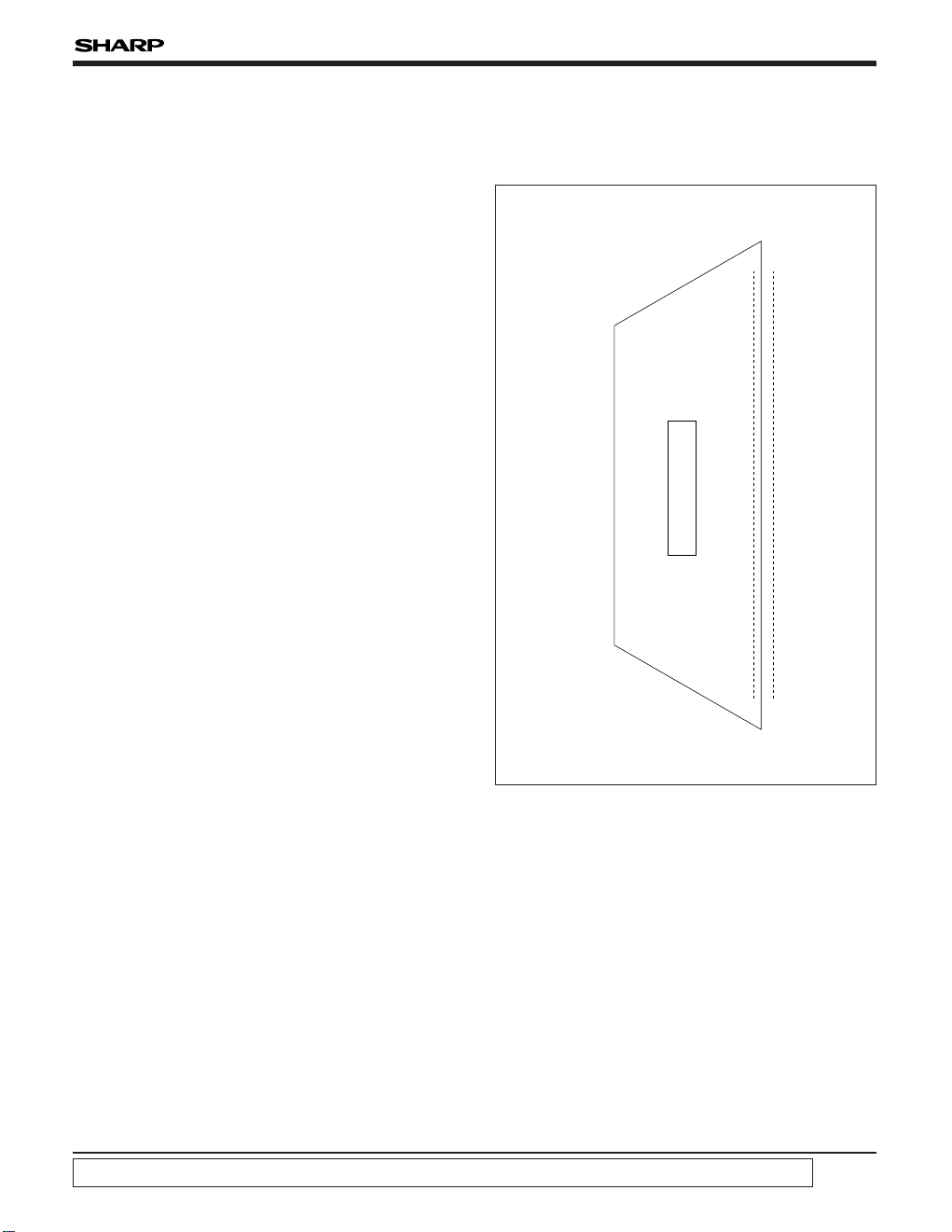
• Package : 264-pin TCP (Tape Carrier Package)
PIN CONNECTIONS
LH1687
LH1687
240-output TFT-LCD Source Driver IC
OS240240
OS
11
CHIP SURFACE
VCCA
VCCL
GNDA
GNDL
TST5
VC
VB
VA
MODE
PS
RL
SAM
CTR
CK
SPIO
SPOI
TEST4
TEST3
TEST2
TEST1
GNDL
GNDA
VCCL
VCCA
264
263
262
261
260
259
258
257
256
255
254
253
252
251
250
249
248
247
246
245
244
243
242
241
264-PIN TCP
TOP VIEW
NOTE :
Doesn't prescribe TCP outline.
Page 2
LH1687
2
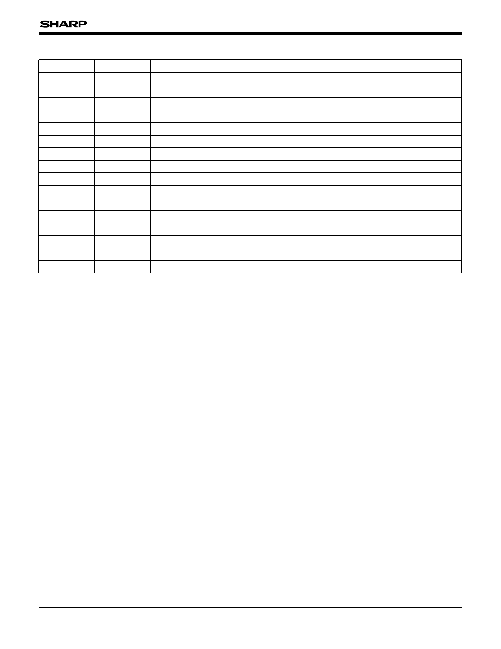
PIN NO. SYMBOL I/O DESCRIPTION
1 to 240 OS
1-OS240 O LCD drive output pins
241, 264 V
CCA – Power supply pins for LCD drive circuit
242, 263 VCCL – Power supply pins for logic circuit
243, 262 GNDA – Ground pins for LCD drive system
244, 261 GNDL – Ground pins for logic system
245 to 248 TST
1-TST4 I IC test pins
249 SPOI I/O Start pulse input/cascade output pin
250 SPIO I/O Start pulse input/cascade output pin
251 CK I Horizontal shift clock input pin
252 CTR I LCD drive circuit operation selection pin
253 SAM I Sampling mode selection pin
254 RL I Sampling sequence selection pin
255 PS I Power save mode setting pin
256 MODE I Video signals form setting pin
257 to 259 V
A, VB, VC I Video signal input pins
IC test pinITST
5260
PIN DESCRIPTION
Page 3
3
LH1687
TST5
VCCAVCCAVCCLVCCL GNDA GNDA GNDL GNDL OS1 OS240
241
260
TST
4 248
PS 255
V
C 259
V
B 258
V
A 257
TST
3 247
TST
2 246
TST
1 245
RL 254
SAM 253
CTR 252
CK 251
SPIO
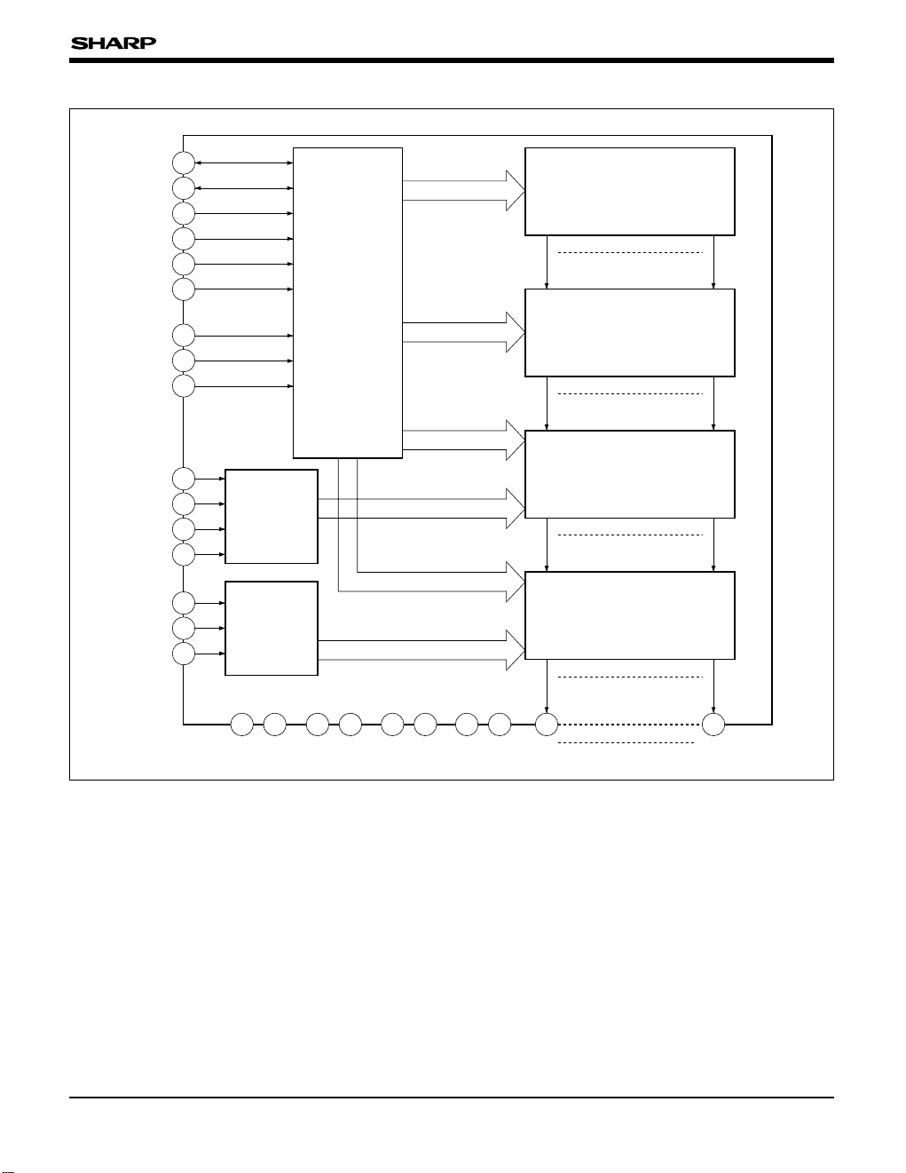
CONTROL
LOGIC
MODE
SETTING
CIRCUIT
BIAS
GENERATION
CIRCUIT
250
SPOI 249
MODE 256
264 242 263 243 262 244 261 1 240
BI-DIRECTIONAL SHIFT
REGISTER
SAMPLING SIGNAL
CREATION CIRCUIT
SAMPLE AND HOLD CIRCUIT
OUTPUT CIRCUIT
1 240
1 240
1 240
1 240
BLOCK DIAGRAM
Page 4
LH1687
4
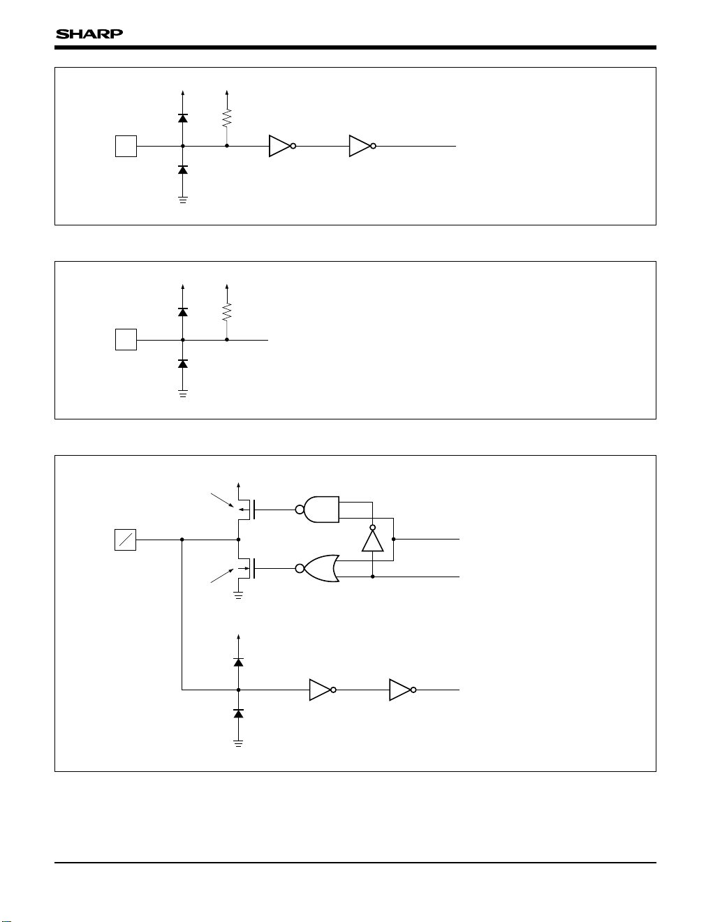
INPUT/OUTPUT CIRCUITS
I
V
CCL
GNDL
To Internal Circuit
Fig. 1 Input Circuit (1)
¿Applicable pins¡
CK, CTR, MODE
I
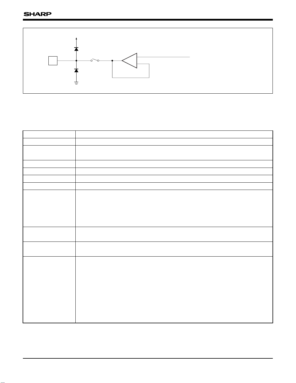
V
CCA
GNDA
To Internal Circuit
Fig. 2 Input Circuit (2)
¿Applicable pins¡
V
A, VB, VC
BLOCK FUNCTION
Control Logic
Used to create signals necessary for each operation mode setting and sampling signal
creation circuits, etc.
Bi-directional Shift
Register
Used as transfer circuit of video sampling start signals.
It is possible to set the direction of sampling start signal sequence OS
1/OS240 or
OS240/OS1 by setting the R/L pin.
Sampling Signal
Creation Circuit
Used to create the sampling signals corresponding to each output pin based on the
sampling start signals transferred by the bi-directional shift register.
Mode Setting Circuit Used to set the form of the video signals to be sent to the sample and hold circuits.
Sample and Hold
Circuit
Used to sample the video signals input from the mode setting circuit at the timing of the
sampling signals and hold the sampling data until the next sampling operation.
Bias Generation Circuit Used to generate bias voltage necessary for output circuits.
Output Circuit
The circuit consists of a push-pull output operational amplifier and outputs the voltage
corresponding to the data held in the sample and hold circuits.
FUNCTIONAL OPERATIONS OF EACH BLOCK
Page 5
5
LH1687
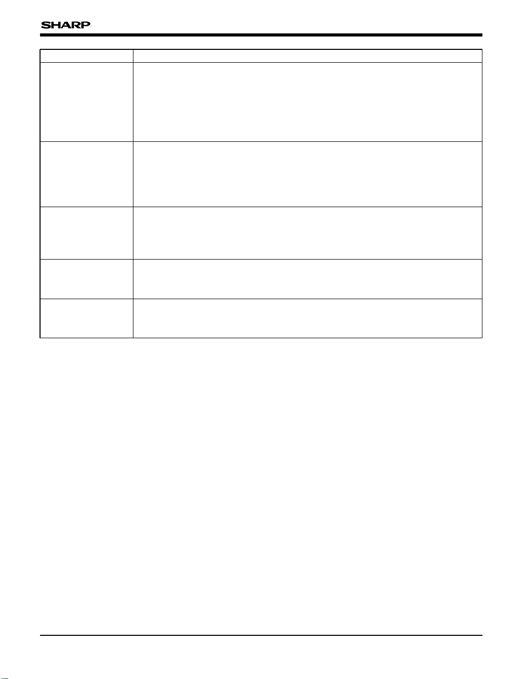
I
V
CCLVCCL
GNDL
To Internal Circuit
Fig. 3 Input Circuit (3)
¿Applicable pins¡
SAM, RL, PS,
TST
1-TST4
I
V
CCAVCCA
GNDA
To Internal Circuit
Fig. 4 Input Circuit (4)
¿Applicable pin¡
TST
5
VCCL
GNDL
Nch Tr
Output Signal
Output Control Signal
VCCL
GNDL
To Internal Circuit
I
O
Pch Tr
Fig. 5 Input/Output Circuit
¿Applicable pins¡
SPIO, SPOI
Page 6
6
LH1687
O
V
CCA
GNDA
From Internal Circuit
Operational
Amplifier
+
–
Fig. 6 Output Circuit
¿Applicable pins¡
OS
1-OS240
FUNCTIONAL DESCRIPTION
Pin Functions
SYMBOL FUNCTION
V
CCL Used as power supply pin for logic circuit, connected to +3.0 to +5.0 V.
V
CCA
Used as power supply pin for LCD drive circuit, connected to +3.0 to +5.0 V.
Must be set to V
CCL ≤ VCCA.
GNDL Used as ground pin for logic circuit, connected to 0 V.
GNDA Used as ground pin for LCD drive circuit, connected to 0 V.
TST
1-TST4 Used as input pins for IC testing, connected to VCCL (high level).
TST5 Used as input pins for IC testing, connected to VCCA (high level).
SPIO
SPOI
Used as input/output pins of cascade operation start signal.
SPIO becomes input pin of operation start signal and SPOI becomes output pin of
operation start signal of next IC when set to R/L = "H".
SPOI becomes input pin of operation start signal and SPIO becomes output pin of
operation start signal of next IC when set to R/L = "L".
CK
Used as horizontal shift clock input pin.
Video signals are sampled in order at the rising and falling edge of CK.
CTR
Used as input pin of selecting video signal sampling circuits and selecting input signal of
output operational amplifiers.
SAM
Used as input pin for setting the selecting of normal sampling operation or 3-point
simultaneous sampling operation.
For normal sampling operation, video signals are sampled into sample and hold circuits
every 1 LCD drive output.
For 3-point simultaneous sampling operation, video signals are sampled into sample and
hold circuits every 3 LCD drive outputs simultaneously.
For either operation, sampling signals are shifted at every rising and falling edge of
horizontal shift clock of CK pin (half clock), and their sampling period is equal to the period
of one clock.
Page 7
LH1687
7
SYMBOL FUNCTION
PS
Used as input pin for setting of power save mode.
LCD drive output pins output voltage corresponding to video signals held in the sample
and hold circuits when set PS to "H".
The LH1687 is set low power mode by setting high-impedance condition and cutting off
current source of LCD drive outputs when set PS to "L".
MODE
Used as input pin for setting video signals for sampling in the sample and hold circuits.
By mode setting circuit, video signals are sampled and output in order of V
B, VA, and VC
when set to "H" and in order of VC, VB, and VA when set to "L" with respect to OS1 to
OS
240 .
OS
1-OS240
Used as LCD drive output pins.
Voltage corresponding to video signals held in the sample and hold circuits is output when
set to PS = "H", and becomes high-impedance condition when set to PS = "L".
Used as input pins of video signals.
V
B, VA, VC, π VB, VA, VC or VC, VB, VA, π VC, VB, VA are input with respect to LCD drive
outputs OS1, OS2, OS3, π OS238, OS239, OS240 by MODE pin setting condition.
V
A
VB
VC
RL
Used as input pin for setting the shift direction of video signal sampling sequence and the
selecting input/output of SPIO/SPOI pins.
Video signals are sampled in order of OS
1/OS240, set SPIO to input of operation start
signal and set SPOI to output of operation start signal of next IC when set RL to "H".
Video signals are sampled in order of OS
240/OS1, set SPOI to input of operation start
signal and set SPIO to output of operation start signal of next IC when set RL to "L".
Page 8

8
LH1687
Functional Operations
(1) Examples of Cascade Sequence
When RL = "H"
SPIO SPOI
OS
1 OS240
Cascade
Sequence 1st
Start Signal
SPIO
SPOI
OS
1 OS240
Cascade
Sequence 2nd
SPIO
OS
1 OS240
Cascade
Sequence n
TFT-LCD Panel
Horizontal Scanning Direction
(n : number of LH1687 used)
When RL = "L"
SPOI SPIO
OS
240 OS1
Cascade
Sequence 1st
Start Signal
SPOI
SPIO SPIO
OS
240 OS1
Cascade
Sequence 2nd
SPOI
OS
240 OS1
Cascade
Sequence n
TFT-LCD Panel
Horizontal Scanning Direction
(n : number of LH1687 used)
Page 9

9
LH1687
(2) Video Signal Mode Setting Function
With MODE pin condition, it is possible to set the
form of video signals corresponding to each output
pin by selecting the mode setting circuit.
When MODE = "H"
When MODE = "L"
Mode Setting Circuit
Output Circuit
V
B VA VC VB VA VC VB VA VC
OS1 OS2 OS3 OS4 OS5 OS6 OS238 OS239 OS240
Mode Setting Circuit
V
C VB VA VC VB VA VC VB VA
OS1 OS2 OS3 OS4 OS5 OS6 OS238 OS239 OS240
Output Circuit
Page 10

LH1687
10
(3) Output Circuit Type
The LH1687 samples video signals by the sample
and hold circuits of 2 systems and outputs the
voltage corresponding to the sampled data by the
input switching operational amplifiers with push-pull
output buffer.
Sample and hold circuits and output circuits are as
shown in the diagram below.
When CTR = "H", the LH1687 samples the data to
system A of the sample and hold circuits and
outputs the voltage corresponding to the voltage
sampled by capacitor B of system B.
When CTR = "L", the LH1687 samples the data to
system B of the sample and hold circuits and
outputs the voltage corresponding to the voltage
sampled by capacitor A of system A.
Therefore, it is usually necessary to repeat the
sampling operation and output operation by
exchanging CTR signal ("H" to "L" or "L" to "H") for
every start signal.
While CTR signal is set to "H" or "L" several times
for start signal, the same voltage is output
continuously.
The output voltage corresponds to the data
sampled by the previous sampling operation.
Timing of operation is as follows.
Also, there is a power save function which makes
high-impedance of the output pin and a reduction in
the current of operational amplifiers possible when
set to PS = "L", but careful attention must be paid
to the displaying quality etc. when using it.
+1
+2
–
Capacitor B
GNDA
GNDA
Sampling
Signal A
Operational Amplifier
+ Output Buffer
Sampling
Signal B
Capacitor A
System B of Sample and Hold Circuits
System A of Sample and Hold Circuits
Output Pin
Video
Signal
Start signal
CTR
System A
System B Sampling 2 Output 2 Output 2 Sampling 4
Sampling 1 Output 1 Sampling 3 Sampling 3' Output 3'
Output 0
Page 11

LH1687
11
(4) Examples of LCD Panel Connection
With the video signal mode setting function of (2), it
is possible to connect LCD panel to the stripe pixel
array panel and delta pixel array panel as shown in
the following examples.
(a) Example of Stripe Pixel Array Panel Connection
VB
LH1687
V
CVA
RBGVideo Signals
1st Line
2nd Line
Sampling
Data
3rd Line
MODE = "H"
MODE = "H"
MODE = "H"
OS
1 OS2 OS3
OS238 OS239 OS240
RGBR BGRB
RGBR BGRB
RGBR BGRB
Video signal input pin
Connection of video signal input pins
VBVA VC
BGRVideo signal
Setting of video signals that are to be sampled by output circuits and MODE pin condition
2nd LINE1st LINE 3rd LINE
RRROS (3n + 1) R
AFTER 4th LINE
"H"
(n = 0, 1, 2, π, 79)
MODE pin setting "H""H" "H"
BOS (3n + 3) BBB
GOS (3n + 2) GGG
Page 12

LH1687
12
(b) Example of Delta Pixel Array Panel Connection
VB
LH1687
V
CVA
RBGVideo Signals
1st Line
2nd Line
Sampling
Data
3rd Line
MODE = "H"
MODE = "L"
MODE = "H"
OS
1 OS2 OS3
OS238 OS239 OS240
RGBR BGRB
BRGB GRBGR
RGBR BGRB
Video signal input pin
Connection of video signal input pins
VBVA VC
BGRVideo signal
Setting of video signals that are to be sampled by output circuits and MODE pin condition
2nd LINE1st LINE 3rd LINE
RRBOS (3n + 1) B and R are alternately selected.
AFTER 4th LINE
"L" and "H" are alternately selected.
(n = 0, 1, 2, π, 79)
MODE pin setting "L""H" "H"
G and B are alternately selected.OS (3n + 3) GBB
R and G are alternately selected.OS (3n + 2) RGG
NOTES :
• Set the MODE pin condition during blanking period.
• Input the horizontal shift clock signal of CK pin by shifting the phase for each line according to the shift of the pixels
connected to the same source bus line.
If the pixels connected to the same source bus line are shifted by half the pixels, change the clock phase 90 degrees.
Clock phase must be changed during blanking period.
Page 13

LH1687
13
Outline of Operation Timing
(1) Overall Operation Timing
Video signals of one horizontal scanning period are
sampled into the sample and hold circuits at the
timing of the internal sampling pulses of each
output circuit, and data corresponding to the
sampled data are output.
Horizontal
Blanking
Period
Effective
Display
Period
Video Signals
Start Pulse
(Horizontal Scanning Start Pulse)
S
1
S240
(Internal Sampling Signals)
PS
OS
1-OS240
(LCD Drive Outputs)
(Power Save Signal)
Output
High-Z
Sampling Data
(j – 1) Output
Output
High-Z
Output
High-Z
Sampling Data
(j) Output
Sampling Data
(j + 1) Output
One Horizontal
Scanning Period
(j)
One Horizontal
Scanning Period
(j + 1)
(2) Timing of Video Signal Sampling
If the normal sampling operation and cascade
sequence is 1st, the video signal sampling (internal
sampling signal Sn (n =
1, 2, π, 240)) is started at the
rising edge of first clock after falling edge of start
pulse.
CK
S1
Start Pulse
(Horizontal Scanning Start Pulse)
S2
(Normal Sampling Operation, Cascade Sequence 1st)
01 2
Video Signal Sampling Start
Page 14

LH1687
14
(2) When RL = "L"
0 1 2 120 121
CK
SPIO
S
1
S2
S239
S240
SPOI
NOTE : S1 to S240 are internal sampling signals of video signal.
NOTE : S1 to S240 are internal sampling signals of video signal.
Timing Chart for Normal Sampling Operation
(1) When RL = "H"
CK
0 1 2 120 121
SPOI
240
S
S239
S2
SPIO
S1
Page 15

LH1687
15
(2) When RL = "L"
0 1 2 40 41
CK
SPIO
S
1-S3
S4-S6
S235-S237
S238-S240
SPOI
NOTE : S1 to S240 are internal sampling signals of video signal.
NOTE : S1 to S240 are internal sampling signals of video signal.
Timing Chart for 3-point Simultaneous Sampling Operation
(1) When RL = "H"
CK
0 1 2 40 41
SPOI
238-S240
S
S235-S237
S4-S6
S1-S3
SPIO
Page 16

LH1687
16
PRECAUTIONS
Precautions when connecting or disconnecting
the power supply
This IC has some power supply pins, so it may be
permanently damaged by a high current which may
flow if voltage is supplied to the LCD drive power
supply while the logic system power supply is
floating. Therefore, when connecting the power
supply, set the logic system input pins (SPIO,
SPOI, CK, CTR, MODE, SAME, RL, PS, TST
1,
TST
2, TST3, TST4) after supplying the voltage to
the logic system power supply pin (V
CCL), and next
supplying the voltage to the LCD drive system
power supply pin (V
CCA). Finally, set the LCD drive
system input pins (V
A, VB, VC, TST5).
When disconnecting the power supply, follow the
reverse sequence.
When connecting or disconnecting the power
supply follow the recommended sequence shown
here.
112
CK
PS
OS
1-OS240
Sampling Data Output Period Output Hi-impedance Period Sampling Data Output Period
Timing Chart for CTR Operation
12 12
CK
CTR
OS
1-OS240
Sampling of System A
&
Output Period System B
Sampling of System B
&
Output Period System A
Sampling of System A
&
Output Period System B
Timing Chart for PS Operation
Page 17

LH1687
17
Power Suplly of Logic System
Input of Logic System
Power Supply of LCD Drive System
Input of LCD Drive System
Connecting The Power Supply
or Input Signals
Disconnecting The Power Supply
or Input Signals
Setting of Input pins
Since 5 pins of SPIO, SPOI, CK, CTR, and MODE
of the input pins are not pulled up or pulled down in
the IC, never use these 5 pins in the "OPEN"
condition.
Since V
A, VB, and VC pins are for inputting video
signals, necessary video signals must always be
input.
Except for V
A, VB, VC, SPIO, SPOI, CK, CTR, and
MODE, all other input pins are pulled up in the IC.
However, to preventing malfunction due to noise
etc., avoid using the "OPEN" condition whenever
possible, and set to "H" level or "L" level.
Input video signals
Input video signals are target for analog signals
(continuous signals).
The input band of video signals is applicable up to
the maximum of 12.5 MHz.
Bypass capacitor
If the noise of a logic system is superposed on
analog circuits such as the sample and hold
circuits, analog characteristics (such as output
voltage deviation and dynamic range, etc.) may
deteriorate. For this reason, insert bypass
capacitors of about 1 µF between V
CCL and GNDL,
V
CCA and GNDA.
Fully evaluate and determine the value of bypass
capacitors with them actually mounted on the LCD
module.
Maximum ratings
When connecting or disconnecting the power
supply, this IC must be used within the range of the
absolute maximum ratings.
Page 18

LH1687
18
RECOMMENDED OPERATING CONDITIONS
PARAMETER SYMBOL APPLICABLE PINS RATING UNIT NOTE
Supply voltage
V
CCLVCCL –0.3 to +7.0 V
1, 2
V
CCAVCCA –0.3 to +7.0 V
Input voltage
V
INL
CK, CTR, SPIO, SPOI, MODE,
RL, SAM, PS, TST
1
-TST
4
–0.3 to VCCL + 0.3 V
Storage temperature T
STG –45 to +125 ˚C
NOTES :
1. TA = +25 ˚C
2. The maximum applicable voltage on any pin with respect to GNDL and GNDA (0 V).
NOTES :
1. The applicable voltage on any pin with respect to GNDL and GNDA (0 V).
2. Ensure that voltages are set such that V
CCL ≤ VCCA.
VINA TST5, VA, VB, VC –0.3 to VCCA + 0.3 V
PARAMETER SYMBOL APPLICABLE PINS RATING UNIT NOTE
Supply voltage
V
CCLVCCL +3.0 to +5.5 V
1, 2
V
CCAVCCA +3.0 to +5.5 V
Input voltage
V
INL
CK, CTR, SPIO, SPOI, MODE,
RL, SAM, PS, TST
1
-TST
4
0 to VCCLV
Operating temperature T
OPR –30 to +85 ˚C
V
INA TST5, VA, VB, VC 0 to VCCAV
ABSOLUTE MAXIMUM RATINGS
Page 19

LH1687
19
NOTES :
1. Start signal :
Cycle t
SP = 63.5 µs, "H" period width tWSP = 80 ns.
CTR signal :
Cycle t
CTR = 127.0 µs, "H" period width tWCTR = 63.5 µs.
Change from "H" to "L" or "L" to "H" is synchronized with
start pulse during blanking period.
CK signal :
Frequency f
CK = 12.5 MHz (duty = 50%)
V
A = VB = VC = 0.1 V to VCCA – 0.1 V
Connect all other pins to high level.
Voltage difference between the average voltage of all
OS output pins in the chip and the output voltage of
each OS output pin. T
A = 25 °C
2. Start signal :
Cycle t
SP = 63.5 µs, "H" period width tWSP = 80 ns.
CTR signal :
Cycle t
CTR = 127.0 µs, "H" period width tWCTR = 63.5 µs.
Change from "H" to "L" or "L" to "H" is synchronized with
start pulse during blanking period.
CK signal :
Frequency f
CK = 12.5 MHz (duty = 50%)
Connect V
A, VB, and VC pins to VCCA.
Connect all other pins to high level.
3. Start signal :
Cycle t
SP = 63.5 µs, "H" period width tWSP = 80 ns.
CTR signal :
Cycle t
CTR = 127.0 µs, "H" period width tWCTR = 63.5 µs.
Change from "H" to "L" or "L" to "H" is synchronized with
start pulse during blanking period.
CK signal :
Frequency f
CK = 12.5 MHz (duty = 50%)
Pin to be set to GND : PS
Connect V
A, VB, and VC pins to VCCA.
Connect all other pins to high level.
PARAMETER
SYMBOL
CONDITIONS APPLICABLE PINS MIN. TYP. MAX. UNIT. NOTE
Input "Low" voltage V
IL CK, CTR, SPIO, SPOI,
MODE, RL, SAM, PS
0
0.3VCCL
V
VIHL
0.7VCCL
VCCLV
Input "High" current
I
IHLVIN = VCCL
CK, CTR, SPIO, SPOI,
MODE, RL, SAM, PS
10 µA
Dynamic range Vp-p V
A, VB, VC 0.1
VCCA – 0.1
V
Supply current
(In power save mode)
ICCA2 100 µA 3
Supply current I
CCL1 VCCL
CK, CTR, SPIO, SPOI,
MODE, V
A, VB, VCVIN = 0 V
I
IL1
Input "Low" current
Input "High" voltage
1.5 mA 2
I
IHAVIN = VCCAVA, VB, VC 10 µA
Input voltage VV
CCA0VINAVA, VB, VC
IIL2 RL, SAM, PS
10 µA
400 µA
1mV20–20OS
1-OS240VOD
Deviations between
output voltage pins
Supply current
(In operation mode)
I
CCA1
VCCA
mA 26.0
ELECTRICAL CHARACTERISTICS
DC Characteristics
(Unless otherwise specified, GNDL = GNDA = 0 V, VCCL = +3.3 V, VCCA = +5.0 V, TOPR = –30 to +85 ˚C)
Page 20

LH1687
20
PARAMETER
SYMBOL
CONDITIONS APPLICABLE PINS MIN. TYP. MAX. UNIT
Clock frequency f
CK
SAM = "H"
CK
12.5 MHz
"H" level clock width t
WHC
SAM = "H" 30.0 ns
Input rise time t
RC
SAM = "H" 10.0 ns
Input fall time t
FC
SAM = "H" 10.0 ns
Start pulse width t
WSP SPIO, SPOI
1
-------f
CK
ns
Start pulse setup time t
SUSP 10.0 ns
Start pulse hold time tHSP 15.0 ns
Start pulse output
delay time
t
DSP CL = 15 pF 20.0 ns
PS signal setup time t
SUPS
1
--------
2f
CK
µs
CTR signal setup
time
t
SUCTR
1
-------2f
CK
µs
SPIO, SPOI, CK
ns30.0SAM = "H"
t
WLC"L" level clock width
µs5.0t
ROutput rise time
µs5.0t
DO
Output transfer delay time
PS
CTR
OS
1-OS240
Output fall time tF 5.0 µs
SPIO, SPOI, CK
1
NOTE
MHz7.0SAM = "L"
SAM = "L" 50.0 ns
SAM = "L" 50.0 ns
SAM = "L" 20.0 ns
SAM = "L" 20.0 ns
2
µs5.0t
FOPPower save fall time
Power save delay time
tDOP 3.0 µs
Power save rise time t
ROP 5.0 µs
NOTES :
1. Start signal :
Cycle t
SP = 63.5 µs, "H" period width tWSP = 80 ns.
CTR signal :
Cycle t
CTR = 127.0 µs, "H" period width tWCTR = 63.5 µs.
Change from "H" to "L" or "L" to "H" is synchronized with
start pulse during blanking period.
CK signal :
Frequency f
CK = 12.5 MHz (duty = 50%)
Connect V
A, VB, and VC pins to VCCA.
Connect all other pins to V
CCL.
Capacity of output load C
L = 150 pF
2. Add load resistor (10 k$) to NOTE 1.
Load resistor is connected to GNDA or V
CCA level as
follows.
Output Pin
10 k$ 150 pF
GNDA
Output Pin
10 k$
150 pF
GNDA
V
CCA
AC Characteristics
(Unless otherwise specified, GNDL = GNDA = 0 V, VCCL = +3.3 V, VCCA = +5.0 V, TOPR = –30 to +85 ˚C)
Page 21

LH1687
21
Timing Chart
90% 90%
90%
90%
90%
10%
90%
90%
90%
90% 90%
90%
10% 10%
10%
10%
10%
10%
90% 90%
10%
10%
90%
10%
10%
90% 90%
10%
90%
10%
10%
10%
10% 10% 10%
tWSP
tDSP
tSUPS tSUPS
tDSP
tSUSP
tHSP tRC tFC
tWLCtWHC
1
f
CK
12 3
1' 2' 3'
LAST – 1LAST – 2 LAST
tDOP
tDOP
tFOP
tROP
Sampling Data Output Output High-impedance
tSUCTR
tDO
tSUCTR
tFO
tDO
tRO
CK
(SPOI)
SPIO Input
CK
CK
PS
(SPOI)
SPIO Output
OS
1-OS240
CK
CTR
OS1-OS240
 Loading...