

Page 1

SHARP
[ SPEC No. 1 E
ISSUE: Aug. 29. 1996
SPECIFICATIONS
Product Type 5 V Drive 240 Outputs TFT-LCD Source Driver’
Model No.
LH1684F
L 0
8 8 1 3
2 1
Kl’his specifications contains 34 pages including the cover and appendix.
If you have any objections,please contact us before issuing purchasing order.
CUSTOMERS ACCEPTANCE
DATE:
BY:-
PRESENTED
Y. SHIOTAw
Dept. General Manager
REVIEWED BY: PREPARED BY:
ENGINEERING DEPARTMENT ! ..--
LOGIC IC ENGINEERING CENTER
TENRI INTEGRATED CIRCUITS (I0 GRQUP 7'::
SHARP CORPORATION ‘-; . -.”
,_ ---. - ._ ;*
- -___.
---
._
,
Page 2

SHARP
GHandIe this document carefully for it contains material protected by international copyright law.
Any reproduction , full or in part , of this material is prohibited without the express written
permission of the company.
OWhen using the produc?s covered herein , please observe the conditions written herein and the
precautions outlined in the following paragraphs. In no event shall the company be iiable for
any damages resulting from failure to strictly adhere to these conditions and precautions.
(1) The products covered herein are designed and manufactured for the following application
LH1684F
areas. When using the products covered herein for the equipment listed in Paragraph
(2) , even for the following application areas , be sure to observe the precautions given
in Paragraph (2) .
* Office electronics
- Instrumentation and measuring equipment
* Machine tools
* Audiovisual equipment
* Home appliances
* Communication equipment other than for trunk lines
Never use the products for the equipment listed in Paragraph (3) .
(2) Those contemplating using the products covered herein for the following equipment which
demands high reliability, should first contact a sales representative of the company and
then accept responsibility for incorporating into the design fail-safe operation , redundancy
, and other appropriate measures for ensuring reliability and safety of the equipment and
the overall system.
* Control and safety devices for airplanes , trains , automobiles, and other
transportation equipment
- Mainframe computers
- Traffic control systems
- Gas leak detectors and automatic cutoff devices
* Rescue and security equipment
- Other safety devices and safety equipment, etc.
(3) Do not use the products covered herein for the following equipment which demands
extremely high performance in terms of functionality , reliability , or accuracy.
- Aerospace equipment
+ Communications equipment for trunk lines
* Control equipment for the nuclear power industry
- Medical equipment related to life support, etc.
(4) Please direct all queries and comments regarding the interpretation of the above three
Paragraphs to a sales representative of the company.
OPlease direct all queries regarding the products covered herein to a sales representative of the
company.
Page 3

SHARP
1.
LH1684F
Contents
Summary . . . . . . . . . . . . . . . . . . . . . . . .._..................................................................... 2
2.
Features . . . . . . . . . . . . . . . . . . . . . . . . . . . . . . . . . . . . . . . . . . . . . . . . . . . . . . . . . . . . . . . . . . . . . . . . . . . . . . . . . . . . . . . . . . . . . . . .
3.
Pin Configuration . . . . . .._........................_............................................_..... 2
Block Diagram . . . . . . . . . . . . .._.__..___.....___._.._..._........_....................................... 3
4.
5.
Description of Pins .................................................................................
5.1 Designation of pins .......................................................................
5.2 Input/output circuit types
6.
Description of Functions and Operations ..................................................
6.1 Functions of pin ............................................................................
6.2 Operation of function ....................................................................
6.3 Outline of operation timing ...........................................................
Timing chart for normal sampling operation .................................... 1 2
6.4
6.5 Timing chart for 3-point simultaneous sampling operation.. ............ 16
6.6 Precautions..
7. Absolute Maximum Ratings . . . . . . . . . . . . . . . . . . . . . . . . . . . . . . . . . . . . . . . . . . . . . . . . . . . . . . . . . . . . . . . . . . .
8. Recommended Operating Conditions . . . . . . . . . . . . . . . . . . . . . . . . . . . . . . . . . . . . . . . . . . . . . . . . . . . 21
9. Electrical Characteristics ........................................................................
9.1 DC characteristics ........................................................................
9.2 AC characteristics .......................................................................
9.3 Timing diagram ...........................................................................
.............................................................................. 20
...............................................................
11
21
21
21
.22
.23
2
4
4
5
6
6
7
10.
1 1..
12.
Example of System Configuration . . . . . . . . . . . . . . . . . . . . . . . . . . . . . . . . . . . . . . . . . . . . . . . . . . . . . . . . . . 24
Example of Typical Characteristics . . . . . . . . . . . . . . . . . . . . . . . . . . . . . . . . . . . . . . . . . . . . . . . . . . . . . . . . .
Package and Packing Specification . . . . . . . . . . . . . . . . . . . . . . . . . . . . . . . . . . . . . . . . . . . . . . . . . . . . . . . 26
25
Page 4
SHARP
LH1684F
1. Summary
The LH1684F is a source driverforthe TFT liquid crystal panel used for LCD unit such as aTV set
and has 240 LCD drive outputs.
The LH1684F samples and holds three video signals of R, G, and B by the sample and hold circuits
at the synchronized with the clock CK , and output simultaneously the output voltage from all
output pins.
2. Features
. No. of LCD drive outputs : 240 outputs
. Supply voltage :
* Output amplitude voltage : 4.0 VP-P (at 5.0 V supply voltage)
+ Sampling frequency :
+ Video signals sampling : Shift direction can be selected.
* Sampling timing : Normal sampling operation and 3-point simultaneous sampling
* Video signal setting :
. Cascade connection :
* Package: 263 pinsTCP (Tape Carrier Package)
* Process configuration :
- Not designed or rated as radiation hardened.
4.5to5.5v
2 0 MHz (MAX)
(OS 1 - OS240 or OS240 - OS 1)
operation can be selected.
Compatible to stripe pixel array panels and delta pixel array panels
by mode setting circuit.
Max. 4 cascades (Internal counting system)
CMOS silicon gate (p-type silicon substrate)
2
3
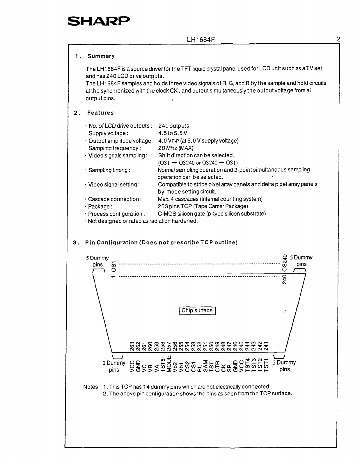
Pin Configuration (Does not prescribeTCP outline)
5 Dummy
Pi0
Notes: 1. This TCP has 14 dummy pins which are not electrically connected.
_-.-----__----__--_-____________________---------------------------------
;5
2. The above pin configuration shows the pins as seen from the TCP surface.
$j? 5Dummy
pins
s:
On
Page 5

SHARP
LH 1684F 3
4. Block Diagram
RL
CSl
cs2
TST
TSTl
TST2
TST3
1
Numerals in circles indicate the pin number.
Bkdirectional shift
Control
logic
. . . . . . . . . . . . . . . . . . . . . . . . . . . .
, --_-_-_-____------_--
6
. . . . . . . . . . . . . . . . . . . . . . . . . . OS240
vcc
Block name I Block function
Control logic
Bi-directional shift register ~ Used as transfer circuit of video sampling start signals.
Sampling signal creation circuit Used to create the sampling signals corresponding to each output
Mode setting circuit / Used to set the form of the video signals to be sent to the sample
Sample and hold circuit
Output circuit
GND
I Used to create signals necessary for controlling cascade sequence
’ and for discharge signal and sampling signals creation circuits, etc.
’ It is possible to set the direction of sampling start signals sequence
/ by setting the FVL pin, from OS1 to OS240 or from OS240 to OS1 .
j pin based on the sampling start signals transferred by the bii directional shift register.
1 and hold circuits.
Used to sample the video signals input from the mode setting circuit I
: at the timing of the sampling signals and hold the sampling datas
I until the next sampling operation.
i The circuit comprises an operational amplifier and an output buffer
1 and outputs the voltage corresponding to the data held in the
/ sample and hold circuit.
OS1
i
I
i
I
Page 6

SHARP
5. Description of Pins
5.1 Designation of pins
LH 1684F
Pin No. I Pinsymbol / I/O
1 to 240 / OS1 to OS240 0 LCD drive output pins
241 j
242 j
1 243 (
244
245,263 ’
246,262 1
247 1 SP
248 ’
249 ~
250 /
251 : SAM ! I
252
253
254 ’
255 ’ Vbl 1 I
256 Vb2 I
257 I
258
259
260 :
261 i
TSTl / I LSI test pin
TST2 / I LSI test pin
TST3 j I LSI test pin
TST4 ~ I LSI test pin
vcc / - Power supply pins
GND i - GNDpins
/ I Horizontal scanning start pulse input pin
CK j I Horizontal shift clock input pin
CTR / I Analog circuit operation selecting pin .
TST j I LSI test pin
Sampling mode selecting pin
RL : I Sampling sequence selecting pin
CSl I I Cascade sequence setting pin 1
cs2 ~ I Cascade sequence setting pin 2 ,
Bias voltage setting pin for output operational amplifiers ’
Bias voltage setting pin for output buffers
MODE 1 I Video signals form setting pin
TST5 j I LSI test pin
VA I Video signal input pin
VB / I Video signal input pin
vc I I Video signal input pin I
Designation
j Remarks
I
I
i
I
I
I
I
I
I
/
/
/
/
! /
I
I
I
1
I
Page 7
SHARP
’ “‘684F
l-1 I IL- .
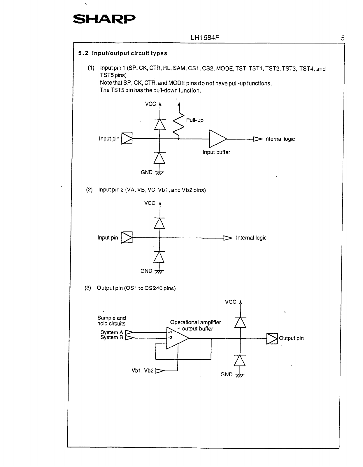
5.2 input/output circuit
(1) Input pin 1 (SP, CK, CTR, RL, SAM, CSl, CS2, MODE, TST, TSTl, TST2, TSTS, TST4, and
TST5 pins)
Note that SP, CK, CTP, and MODE pins do not have pull-up functions.
TheTST.5 pin has the pull-down function.
Input pin
(2) Input pin 2 (VA, VB, VC, Vbl , and Vb2 pins)
types
Input buffer
Internal
logic
Input pin BBp fnternal logic
Output pin (OS1 to OS240 pins)
(3)
vcc
Sample and
hold circuits
Operational
--,:I:-- 7k
ampwer
tput buffer
4
t
Outpu
pin
Page 8

SHARP
Description of Functions
1 Functions of
Pin symbol
vcc Used as power supply pin, which is normally connected to +5.6 V.
GND / Used as GND pin, which is connected to OV.
TST : Used as pin for LSI testing. Must be connected to VCC.
TSTl to TST4 I Used as pins for LSI testing. Must be connected to VCC.
TST5
SP
CK
CTR i Used as input pin of selecting video signals sampling circuits and selecting input
SAM Used as input pin for setting the selecting of normal sampling operation or S-point
i-
RL
CSl, cs2 1 Used as input pins for setting of chip cascade sequence.
pin
: Used as pin for LSI testing. Must be connected to GND.
j Used as input pin of horizontal scanning start pulse.
j Used as input pin of horizontal shift clock.
/ Video signals are sampled in order at rise timing and fall timinglof CK.
/ signals of output operational amplifiers.
j simultaneous sampling operation.
i For normal sampling operation, video signals are sampled in order 7 LCD drive output.
For 3-point simultaneous sampling operation, video signals are sampled in order
I simultaneously 3 LCD drive outputs.
j For either operation, sampling signals are shifted at every rise timing and fall timing of
j horfzontal shift clock of CK pin (half cfock) , and their sampling perfod is equal to the
period of one clock.
Used as input pin for setting the shift direction of video signals sampling sequence.
~ Video signals are sampled in the order of from OS1 to OS240 when set to “H” and in tht
order of from OS.240 to OS1 when set to “L”.
/ Set chip cascade sequence as shown in the table below.
and
Operations
Pin functions
’ Cascadesequence ’ cs1 cs2
I
I
; For details, refer to “6-2. Operation of function” on page 7.
MODE ’ Used as input pin for setting form of video signals for sampling.
/ By mode setting circuit, video signals are sampled and output with respect to OS1 to
i OS246 in the order of VB, VA, and VC when set to “H” and in the order of VC, VB, and
VA when set to ‘IL”.
/ For details, refer to “6-2. Operation of function” on page 7.
1 Do not use this function in “OPEN” condition.
Vbl r Used as pin for setting the bias voltage of operational amplifiers in output circuits.
Vb2
VA, VB, VC Used as input pins of video signals.
OS1 to OS240 j Used as LCD drive output pins.
i Used as pin for setting bias voltage of buffers in output circuits.
/ VB, VA, VC, ._. VB. VA, VC or VC, VB, VA. . . .
; drive outputs OSl, OS2,OS3. . . . 08238,05239,OS240 by MODE pin setting
1 condition.
i All output pins discharge simultaneously at the timing of internal
; after discharge is completed, they output voltage corresponding to sampled video
: signals.
1st H I H
I
2nd
3rd
4th / L j L
L ! H
I
H ; L
VC, VB, VA are input with respect to LCD
discharge signal and
Page 9
-.
SHARP
6.2 Operation of function
(1) Examples
of cascade
When RL=“H”
Cascade Cascade Cascade Cascade
When RL=“L”
LH1684F
sequence
Horizontal scanning direction e
I
I
TFT-LCD panel c‘,
Horizontal scanning direction
TFT-LCD panel =>
7
e
CSl=‘H’
CSP=‘H’ CSP=‘H’
I
--I
Cascade
sequence 1st sequence2nd sequence 3rd
CSl=‘L
II
Cascade
II
CSl=‘H’
CSL=‘L
Cascade
Cascade
sequence 4th
(2) Video signal mode setting function
With MODE pin condition, it is possible to set the fon of video signals corresponding to each
output pins by selecting the mode setting circuit.
When
MODE=“H”
j..
I I I I
OS OS OS OS OS OS
1 2 3 4 5
6
Output circuit
When MODE=‘L”
Mode setting circuit
Output ciicuits
Page 10

LH 1684F
(3)
Output circuit type
The LH1684F samples video signals by the sample and hold circuits of 2 systems and outputs
the voltage corresponding to the sampled data by the input switching operational amplifiers.
Sample and hold circuits and output circuits are as shown in the diagram below.
When CTR=“H”, the LH1684F samples the data to system A of the sample and hold circuits
and outputs the voltage corresponding to the voltage sampled by capacitor B of system B.
When CTR=“L”, the LH1684F samples the data to system B of the sample and hold circuits
and outputs the voltage corresponding to the voltage sampled by capacitor A of system A.
System A of sample and hold circuits
r---------------------------------.
L_____________---__________________
System B of sampie and hold circuits
.1
8
Therefore, it
is necessary to repeat sampling operation
and output operation by exchanging
CTR signal to “H” and “L” for every SP signal, usually.
When CTFI signal is set to “H” or “L” several times for SP signal, the same voltage is output
continuously during such period.
The output voltage corresponds to the data sampled by the previous sampling operation.
Timing of operation is as follows.
SP
CTR
I
4 4
System
A
System B output 0 Sampling
Sampling 1 output 1
--A
Sampling
2 output 2 output 2 Sampling 4
3 Sampling 3’ output 3’
Page 11
SHARP
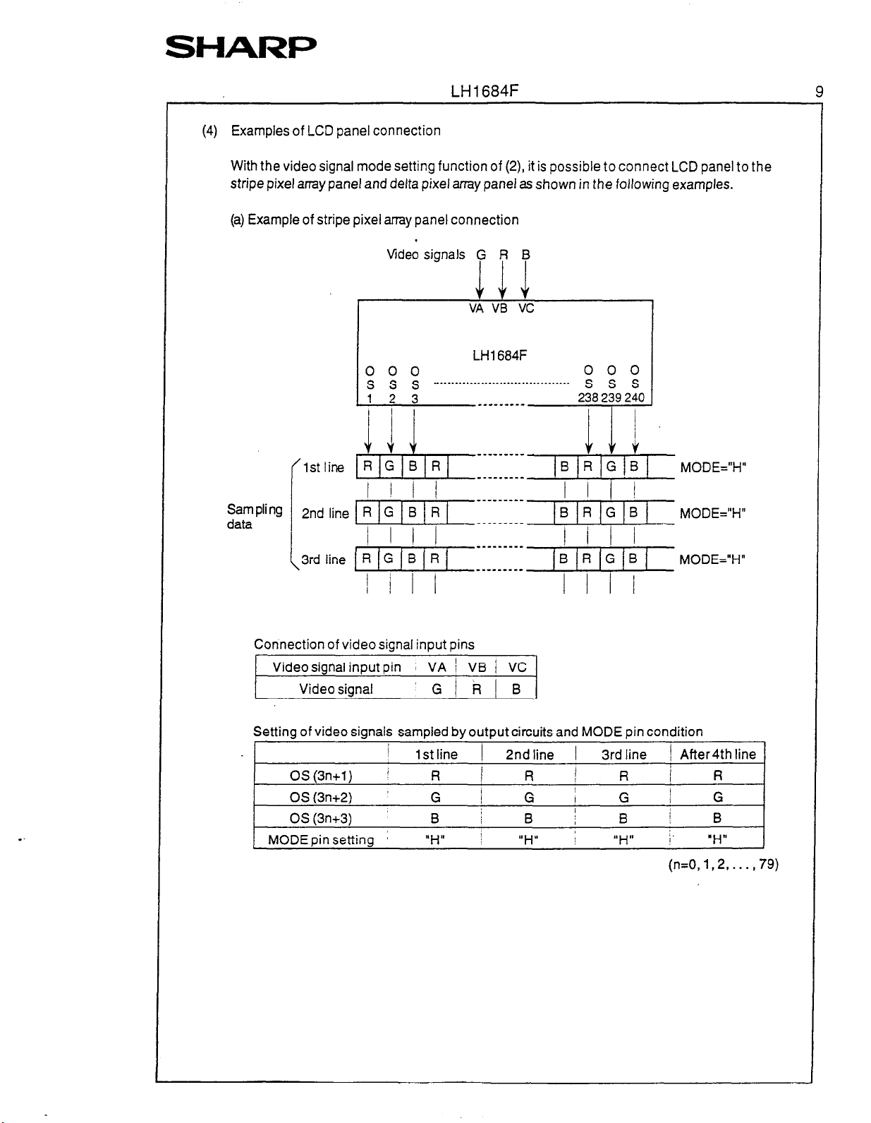
(4) Examples of LCD panel connection
With the video signal mode setting function of (2) it is possible to connect LCD panel to the
stripe pixel array panel and delta pixel array panel as shown in the following examples.
(a) Example of stripe pixel array panel connection
‘1st line
LH1684F
Video signals p 7 f
Sampling
data
Connection of video signal input pins
Setting of video signals sampled by output circuits and MODE pin condition
2nd line R G B R
3rd line R G B R
Videosignal input pin ; VA / VB 1 VC
Video signal ‘G/RIB
OS(3n+l) j R / R j R ; R
OS (3n+2) G
OS (3n+3) B i
MODE pin setting
m::;:-;;:: MODE=“H”
I 1 I I
~:]::-:::: IB IR IG /B 1
I I I I
1
lstline I 2nd line 1 3rd line
I
U,,” 1
1 ; 1 d 1; 1 Ii /
I i I
i
I I I I
G
B B j
“,,” ;
I
I G
/
“H” ! “H”
MODE=“H”
/ After 4th line
/
I
;.
(n=O, 1,2,. . . ,79)
G
B
Page 12

SHARP
(b) Examples of delta pixel array panel connection
LH 1684F
Sam pli ng
data
1st line
f
2nd line
0 0 0
s s s
1 2 3
b b IG b 1
. . . . . . . . . . . . . . . . . . . . . . . . . . . . . . . . . . . . . s s s
+&.$I ___---- L$g&&
3rd fine
(
Connection of video signal input pins
Videosignal input pin ’ VA j VB ’ VC /
Video signal
G’R,B;
VA VB
LH1684F
___--_--_
VC
0 0 0
238 239 240
MODE=“H”
MOD E=“L”
MOD E=“H”
Setting of video signals sampled by output circuits and MODE pin condition
1 lstline 2nd line / 3rd line I
OS(3n+l) !
OS(3n+2) / G R
OS(3n+3) / B i
MODE pin setting ’
Note 1.
Note 2. input the horizontal shift clock signal of CK pin by shifting the phase for each line
Set the MODE pin condition during output discharge period.
according to the shift of the pixels connected to the same source bus line.
ff the pixels connected to the same source bus line is shifted by half the pixels, change
the clock phase 180 degrees.
Clock phase must be changed during output discharge period.
R B ; R / B and Rare alternately selected.
;
G
“HO, j “L” ; a,,”
G
B / G and B are alternately selected.
!
/ R and G are alternately selected.
[ ‘L” and “H” are alternately selected. !
After4th line
(n=O, 1,2,. . . ,79)
Page 13

6.3 Outline of operation timing
(1) Overall operation timing
Horizontal Effective
blanking display
period period
< >
Video signals
scanning period scanning period
4
DIS
(Internal discharge signal)
Sl
s240
(Internal sampling srgnals)
LH1684F
One horizontal One horizontal
0‘) ti+l)
.1
11
>
OS1 to OS240
(LCD drive outputs)
Output diszge period Output diszge period Output diszrge period
Sampling data Sampling data Sampling data
(j-l) output 0’) output
(j+l) output
Video signals of one horizontal scanning period are sampied into the sample and hold circuits
at the timing of the internal sampling pulses of each output circuits, outputs are discharged
once on the GND level by the internal discharge signal, and data corresponding to the
sampled data are output.
This discharge operation is performed simultaneously for all output pins.
(2) Timing of output discharge and video signal sampling
The output discharge period (period “H” of the internal discharge signal DIS) is after3 cycles
of clock CK from the “H” period of start pulse SPD. Therefore, the output discharge period is
almost the same period as the “H” period of start pulse SPD.
lfthe normal sampling operation and cascade sequence is lst, the video signal sampling
(internal sampling signal Sn) is started after 15 cycles of clock CK following the fall of start
pulse SPD.
CK
SP [
DIS
Sl (Normal sampling operation, cascade sequence 1 st) Video signal sampling start
c--- Output discharge period -
-
Page 14

LH 1684F
6.4 Timing chart for normal sampling operation
(1) When RL=“H”, CSl=“H”, and CS2=“H”
si39
S240
(Internal samplrng signals) i
OS1 to OS240
12
j
Sampling data ’ Output discharge !
- .
output period period
(2) When RL=“H”, CSl =“L”, and CS2=“H”
S240
(Internal samplrng signals);
OS1 to OS240
Sampling data output period
Sampling data - ’ Output discharge !
output period
period
Sampling data output period
Page 15

(3) When RL=“H”, CSl =“H”, and CS2=“L”
CK
SP
DIS
s240
(Internal sampltng slgnatsj /
OS1 to OS240
LHI 684F 13
Sampling data ’ Output discharge ! -
output period period
(4) When RL=“H”, CSl=“L”, and CS2=“L”
DIS
(Internal discharge signal) ;
Sl
s2
si39
s240
(Internal sampling slgnaa) i
OS1 to OS240
Sampling data output period
Sampling data ’ Output discharge ’
output period period
Sampling data output period
Page 16

LH 1684F
When RL=“L”, CSl=“H”, and CS;Z=“H”
DIS
Sl
(Internal sampling slgnais) ;
OS1 to OS240
14
Sampling data
output period
(6) When RL=“L”, CSl=“L”, and CS2=“H”
Sl
(Internal sampling slgnaw i
OS1 to OS240
’ Output discharge ! Sampling data output period
period
Sampling data ’ Output discharge ! Sampling data output period
output period period
Page 17

(7) When RL=“L”, CSl =“H”, and CS2=“L”
CK
SP
Sh
Sl
(Internal sampling srgnals) j
OS1 to OS240
Sampling data ’ Output discharge ! Sampling data output period
output period
(8) When RL=“L”, CSl =“L”, and CS2=“L”
iiternal sampling signals) i
OS1 to OS240
period
Sampling data
output period
’ Output discharge ’
period
Sampling data output period
Page 18

SHARP
LH 1684F
6.5 Timing chart for 3-point simultaneous sampling operation
(1) When RL=“H”, CSl=“H”, and CS2=“H”
S238 to S240
(Internal sampling srgnals)
OS1 to 240
16
Sampling data ’ Output discharge ’
output period period
(2) When FiL=“H”, CSl=“L”, and CS2=“H”
CK
SP
S238 to S240
(Internal sampling signals)
OS1 to 240
d
Sampling data output period
.‘4
Sampling data ’ Output discharge ’
output period period
Sampling data output period
Page 19

SHARP
(3) When RL=“H”, CSl=“H”, and CS2=“L”
CK
S4 to S6
5135 to S237
S238 to 5240
(Internal sampling slgnars)
OS1 to 240
u -I
Sampling data ’ Output discharge !
output period period
LH 1684F
17
1 j
Sampling data output period
(4) When RL=“H”, CSl=“L”, and CS2=“L”
CK
SP
DIS
(Internal discharge signal)
Sl to 53
S4 to S6
S235 to S237
S238 to 5240
(Internal samplrng srgnay
OS1 to 240
.‘I
Sampling data ’ Output discharge r Sampling data output period
output period
period
Page 20

SHARP
(5) When FiL=“L”, CSl=“H”, and CS2=“H”
CK
SP
DIS
S240 to S238
S237 to 5235
S6 to S4
s3 to Sl
(Internal sampling signals) /
LH1684F
, I
OS1 to 240
Sampling data Output discharge ! Sampling data output period
output period period
(6) When RL=“L”, CSl=“L”, and CS2=“H”
DIS
(Internal discharge signal)
5237 to S235
S&OS4
s3 to Sl
(Internal sampling signals)
-I-
OS1 to 240
Sampling data ’ Output discharge !
output period period
Sampling data output period
Page 21

SHARP
(7) When RL=“L”, CSl =“H”, and CS2=“L”
CK
SP
DIS
s3 to Sl
(Internal sampilng slgnats)
OS1 to 240
Sampling data ’ Output discharge ! Sampling data output period
output period
period
LHI 684F
1
19
(8) When RL=“L”, CSl =“L”,
DIS
(Internal discharge signal)
OS1 to 240
Sampling data ’ Output discharge ’
output period period
and
CS2=“L”
Sampling data output period
Page 22

6.6 Precautions
(1)
Setting of external voltage of
The LHl684Fdoes not have the bias voltage setting circuit forthe output operational amplifiers
and the output buffers. Therefore it is necessary to input the suitable voltage to Vbl pin and
Vb2 pin.
Set the voltage value to an optimum value in the range of Vcc to GND as shown in the diagram
below, fully evaluating the current consumption, picture quality, etc.
(Example of bias circuit)
LH1684F
Vbl
and Vb2 pins
t----r> Vbl, Vb2
20
Set the resistance to Rl +R2=50 kfI
(2) Setting of Input pins
Since 6 pins of SP, CK, CTR, MODE, Vbl , and Vb2 of the input pins are not pulled up or
pulled down in the LSI, never use these 6 pins in the “OPEN” condition.
Since VA, VB, and VC pins are for inputting video signals, necessary video signals must be
input always.
Except VA, VB, VC, Vbl , Vb2, SP, CK, CTR, and MODE, all other input pins are pulled up or
pulled down in the LSI. However,because of preventing malfunction due to noise, etc., avoid
using the “OPEN” condition whenever possible, and set to “H” level or “L”level.
(3) Input video signals
Input video signals are target for analog signals (continuous signals).
The input band of video signals is applicable up to the maximum of 10 MHz.
(4) Bypass capacitor
lfthe noise of alogicsystem is superposed on analog circuits such as the sample and hold
circuits, analog characteristics (such as output voltage deviation and dynamic range,etc.) may
deteriorate. Forthis reason, insert bypass capacits or of about 1 pF between VCC and GND.
Fully evaluate and determine the value of bypass capacits orwith actually mounted on the
LCD panel.
L
Page 23

SHARI=
Absolute Maximum Ratings
7.
I
I
I
j Storage temperature /
Parameter / Symbol Condition i Rating Unit /
Supply voltage / vcc Ta=+25 “c / -0.3to+7.0 : V /
Input voltage /
VINCC
Tstg / 1 -45to+125 j “c /
Note:Standard voltage is GND (0 V).
8. Recommended Operating Conditions
I
1
I
I
Parameter
i Symbol ’ Condition / Rating
Supply voltage / vcc : +4.5to+5.5 i u
Input voltage
j
VINCC
1
/ Operating temperature i Topr /
Note:Standard voltage is GND (0 V).
9. Electrical Characteristics
9.1 DC characteristics
I H1684F
Ta=+25 “c j -0.3toVcc+0.3 v I
; Unit /
!
0 to ucc
: v j
j -3Oto+85 : “c /
21
1
I
I
/ Measuring /
Parameter !Symboli condition / MIN / TYP j MAX
Input “L” voltage
Input “H” voltage
Input “L” current ! 1.0 / PA / Pinsl,and3 I
Input “H” current
/
!
I
1
Dynamic range
! Output voltage deviation 1 VOD / (Condition 1);
1 VIL )
j ‘/IH /
/ 1111 1
vIN=ov
I llL.2 /
1 llH1 / viN=vCC i
j III-I2 )
j UPP /
I
0 /
i
/ 0.7vcc;
j
I
1
I
/ 0.5 1
I 0.3vcc
i vcc v j
j
I
/
~
1 50.0 PA j
j ,b:“, 1 ILL 1 Pinspil,(sa3nd2 j
j 50.0 j mV ( OS1 toOS240
Current consumption ) ICC 1 (Condition 2)j j 6.0 j mA 1
I
Unit 1 Applicable pin !
U / Pins1,2,and3’
I
Pins 2
’ /vcc-0.5 u / VA,VB,VC !
vcc /
Unless otherwise specified, GND=O V, Ubl =Vb2=2.0 U, Ta=-30 to +85 “C.
[Applicable pins]
(Pin 1) Applicable to CK, CTR, SP, and MODE pins.
(Pin 2) Applicable to RL, CSl , CS2, SAM, TST, and TSTl to 4 pins.
(Pin 3) Applicable toTST5 pin.
[Measuring condition]
(Condition 1) SP signal :
CTR signal : Cycle
Cycle tSP = 63.5 ps, “H’ period width
tCTR
= 127.0 ps, ‘H” period width
twHP =
tWHCT =
5.0 JLS
63.5
ps
Change from “H” to “L” and vice versa during “H” period of SP signal.
CK signal : Frequency
fCK =
10.0 MHz
Pin to be set to 2.0 V : Vbl , Vb2
Pin to be set to GND : TST5
UA=VB=UC=0.5 U to Ucc-0.5 U
Connect all other pins to Vcc.
Difference between the output voltage mean value of all OS output pins in the chip
and the output voltage of each OS output pin.
Ta=25 @
/
I
Page 24

LHl684F 22
(Condition 2) SP signal :
CTR signal : Cycle
CK signal : Frequency fCK = 10.0 MHz
Pin to be set to 2.0 V : Vbl , Vb2
Pin to be set to GND : TST5
Connect all other pins to Vcc.
9.2 AC characteristics
_~
Parameter / Symbol’ condition : MIN ) TYP /
Clock frequency
“H” level clock width
“L” level clock width
Clock rise time /
Clock fall time
Dabsetuptime / tsu j / 30.0 i
Data holdtime j tH
I
Pulse setup time
Pulse holdtime
“H”level pulse width
Pulse alteration time ! trfP I
Output transfer delay time /
Output risetime /
Output fall time /
Cycle tS? = 63.5 us, “H” period width
~CTR
= 127.0 us, “H” period width
Change from “H” to “L” and vice versa during “H” period of SP signal.
I
fCK
tWHC i
! Measuring
SAM=“H” j 40.0 1 j
/
j SAM=“L’ / 90.0 1 /
j tWLC :
I
, SAM=“L” i 90.0 j !
trC
1
I
/ trc
/
SAM=“H” I 40.0 ! /
j SAM=“H” I
SAM=“L”
I
I
j SAM=“H” 1 /
j SAM=“L” / /
; 30.0 !
I tsup
j tHP
/ tWHP ;
tdl
, tm ; Gondition)l 1
tr j j 1.5
tf :
0.5 / /
I 0.5 /
I 5.0 I /
I
t
I
/
( 1.0 / 2.0 1 ps /
tWHP =
,
5.0
ps
tWHcT
= 63.5 us
!
MAX 1 Unit / Applicable pin
,
CK
j ns j
I
I
I
, ns /
/ ns I
/ ns j
/ 10.0 / ns CK, SP
: 35.0 j ns
/ 10.0 / ns j
j 35.0 j ns
I
I
ns
j ns /
SP, CTR
/
/ P I
/psj SP ~
i 1.0 )
pS
1 CTR ’
1 0.7 / ps / SP j
1 2.0 j ps _ I OS1 toos240 :
/ 3.0 / ps j OS1 toos240
/
,
Unless otherwise specified, GND=O V, Vbl =Vb2=2.0 V, Ta=-30 to +85”C.
[Measuring condition]
(Condition) SP signal :
CTR signal : Cycle
Cycle tsP = 63.5 ps, “H” period width
tCTR
= 127.0 ps, “H” period width
tWHP =
twHCT =
Change from “H” to “L” and vice versa during “H” period of S P signal.
CK signal : Frequency fcK = 10.0 MHz
Pin to be set to 2.0 V : Vbl , Vb2
Pin to be set to GND : TST5
Connect all other pins to Vcc.
Capacity of output load CL=~ 5OpF
5.0 ps
63.5 ps
Page 25

9.3 Timing diagram
LH 1684F 23
CK
CTR
OS1 to
OS240
trC, tWHC
tdl
tic tWLC
>-4 F
tWHP
I
Page 26

SHARP
10. Example of System Configuration
“aA
r
LHI 684F
24
LrR
SP
ac
:
;R
+g LL
b’
“al
4
i&E
I
VA
I
VB
) vc
t-- SAM
i TST
TSTl to 1 OS2 TST5
m
4 vcc
MODE
o(
SP
osao-
0%-S0S238-
;
$ :
(D i
fj i
OS3 OS1 -
Controller z
Page 27

11. Example of Typical Characteristics
LH1684F
25
Parameter /
Basic gate propagation
delay time
/
I GND=O V,Vcc=+5.0 V, ’
I *
Conditions 1 MIN 1 TYP I MAX / Unit
Ta=+25 @
I I’Oi In=
Page 28

LH1684F
12. P.4CKXGE AND PACKING SPECIFICATION
1. Package Outline Specification
Refer to drawing No. SPN4701-00
2. Markings
The meanings of the device code printed on each tape carrier package are as follows.
(1) Date code (example) : 5 3 8 D 0
a) denotes the last figure of Arino Domini (of production)
b) denotes the week (of production)
c) denotes factory code (of production)
d) denotes the number of times of alteration
3. Packing Specifications
---a) b) c) d)
26
3-2 Packing Form
a) Tape carrier package(TCP) is wound on a reel
with separator and the ends of them are fixed
with adhesive tape.
b) A label indicating production name, lot no.
and quantity is stuck on one side of the reel.
c) The reel and silica gel is put in a laminated
aluminium bag. Nitrogen gas is enclosed in
the bag and the bag is sealed. The same
label(b) is affixed to the bag. The bag is put
in a carton and the same label(b) is affixed
to one side of the inner carton.
d) 5 inner cartons are put in an outer carton and the same
label(b) is affixed to one side of the outer carton.
3-3 Other
(1) The length of the TCP is typically 40 m per reel, but this may change in
accordance with the inventory quantity.
(2) Faulty devices is conpletely punched out at the part of the device.
(3) The maximum number of continuous faulty devices is 9.
ISSUE DATE AUG 28.1996 APPROVE CHECK DESIGN
ISSUE NUMBER H8801
S/C NUMBER
4
* Specification of label
TYPE
Production name
Lot No:
QUANTITY Quantity
LQT(DATE) Shipping date
I
(NO-W
Page 29

SHARP
LH1684F
4. Cautions concerning handling.
Althrough the strength of the device has been verified in accodance with the test
method shown below, do not subject the resin parts or the slit terminals to any
excessive bending or pressure.
Indicate as moment M.
M=FXL (N-m)
M=1.47X 10e3 N*m MAX.
(for both + B and - 0)
5. Cautions concerning stora,oe.
- When storing the product, it is recommended that it be left in its shipping package.
After the seal of the packin, 0 bag has been broken, store the products in a nitrogen
atmosphere.
* Strage conditions
27
Straoe state Straoe conditions
Unopened(less than 60 davs)
.
.
. . . . . . . ..-.-..-.-..---...---.-..‘.....----.---..-.----..-.--.--......-.
After seal of broken
* Don’t store in a location exposed to corrosive gas or excessive dust.
- Don’t store in a location exposed to direct sunlight or subject to sharp changes in
temperature.
* Don’t store the product such that it subjected to an excessive load weight, such as
by stacking.
* Deterioration of the plating may occor after long-term storage, so special‘ care
is required.
It is recommended that the products be inspected before use.
6. Other cautions.
- Immediately after opening the moisture-proof packing, the mesurement will shrink
slightly. In oder to return the mesurements to those shown in the drawing, it is
nessesary to store the product for at least 48 hours at a temperature of 20’ to 25°C
and humidity of 50 to 60%.
Temperature: 5 to 30°C; humidity : 80% RH or less.
Room temperature, dry nitrogen atomosphere.
_____._-_-....____-_-..------------.-.
Page 30

SliARf=
LH1684F
7. External appearance inspection
ion of the rsternal aopearance of the packare
Item Insoection standards
I. Exposure of the inner lea . Faulty if.the chip or inner leads are completely
and device holes
2. Air bubbles
3. Seal resin area
&. Seal resin thickness
5. Adherance of resin or
foreign matter except
the seal resin area.
i. Undrside of the chip
‘. Scratches, cracks and
chipping in the tape carrie
L Pattern deformation
9. Discoloration
0. Markings
exposed.
. Faulty if the device holes are not completely
filled with resin. ’
*Faulty if there are air bubbles extending as far as
the suaface of the chip.
*Faulty if there are air bubbles at the inner leads.
-Faulty if the area of the seal resin area exceeds
the specifications.
* Faulty if the thickness of the device exceeds the
specifications.
‘Faulty if there is anything adhering to the tin
plating.
‘Faulty if any resin or forein matter adhered to the
copper pattern is wider than the width of the
pattern. (If the forein matter is easily moved, it is
not a cause for concern.)
Faulty if there are any cracks in the chip.
Faulty if there is any chipping in the underside of
the chip that is lager than one-half the thickness
of the chip.
Faulty if adherance of the resin to the underside
of the chip that causes the thickness of the device
exceed the specifications.
Faulty if there are any scratches exposing the
sustrate (chip, pattern. or inner leads) at the seal
resin.
Faulty if there are any scratches extending as far
as the copper foil at the sorder resists.
Faulty if there are any cracks or chipping at the
perforations.
FdUky
if the pattern overhanging the slits is
markedly deformed
Faulty if the tin plating is markedly discolored.
Faulty if the cover coating is markedly
discolored.
Faulty if the markings are illegible.
e shown below.
Remarks
t
Faulty
Jpperside: 16.5 X 5.2 mmMAX
Jnderside: 16.5 X5.2 mmMAX
Upperside:0.30 mmMAX
Underside:0.75 mmMAX
Total thickness: 1.20 mmMAX
T/ZMAX
Creased
n
Faulty
f
Faulty
28
1
1. Missing parts of output
leads
12. Other
Faulty if the width of the output lead is reduced
to less than one-half of the standard.
Faulty
if copper foil remnants reduce the clearanc
between the output leads to less than two-thirds o
the standards.
FdUlty
if there is any warping, twisting. bending,
etc.. of the tape that would impair use.
Faulty if there are no indication holes at the noneffective indication holes.
Page 31

SHARI=
SPECIFICATION OF LABEL
LH 1684F 29
LOTCDATE)
SHIPPNIG DATE
REEL
A d405,
‘IZE B
.TERIAL TREATED PLASTIC MATERIAL CARDBOARD /q, j&...??k
ANTI-STATIC
0127
C 36
INNER CARTON
L
SIZE w
H
420
4-20
50
DATE AUG. 31. 1995
UNIT
APROVE CHECK DESIGN DRAWINGNo.
mm
T1TLE OF TCP PACKING
REEL AND INNER CARTON
KPN 023
ASSEMBLY ENGNEERING
SHARP CORPORATION
DEPT.
Page 32

I
SliARP
LH1684F
30
I LAM1 NATED BAG
PACKING VIEW OF
Page 33

SHARP
LH1684F
31
LABEL
FL
IC GROUP
SHARP CORI
‘ORATION
RAWING
OUTER CARTON
NO
Page 34

LH1684F
32
I
NOTES: 1. REEL WINDING
ANTI-STATIC
TREATED PLASTIC
PATTERNS I DE
**.O(GOOD DEVICE HOLE)
0.6CSL)
VII I
I,. 909(SL) I
[24.5&E. L)l
22. aksL)
1, 909(SL) I 0. S(SL)
YSEPARETOR
2. RESIN AREA OF FRONT AND
BACK SURFACE IS 16. 5X5. 2mmhAX).
3. E. L. MEANS ASSUMED EXCISING LINE.
4.SL MEANS DIMENSION OF PUNCHlNG
HOLE AND ITS TOLERANCE IS k0. 05mm.
5. SR MEANS DIMENSION OF SOLDER
RESIST AND ITS TOLERANCE IS CO. 3mm.
6. POTTING RESIN IS SL5.
0.75MAX.
CROSS SECTION OF OUTPUT LEADS tj
.
m
:
r:
R R
(D *
d d _*----.
!EL
,- -\
I
:
El Ii
\ ,
- -_e*
\
\
I
0. 4 to. 02
0. 6 to. 02
I
OUT LINE
DRAWING OF
 Loading...