

Page 1
CORPORATION
Fast Buffer
LH0033 / LH0033C
FEATURES
Slew ra te. . . . . . . . . . . . . . . . . . . . . . . . . . . . . . . 1500V/µs
••
Wide range single or du al suppl y op era tion
••
Bandwi dt h . . . . . . . . . . . . . . . . . . . . . . . . . . . . . . 100MHz
••
High output drive. . . . . . . . . . . . . . . ±10V wi th 50Ω l oad
••
Low phase non-l inear ity . . . . . . . . . . . . . . . . 2 degrees
••
Rise times . . . . . . . . . . . . . . . . . . . . . . . . . . . . . . . . . . 3ns
••
High input resistance:. . . . . . . . . . . . . . . . . . . . . . . 1010Ω
••
High outp ut curr ent ( peak ) . . . . . . . . . . . . . . . . . 250mA
••
APPLICATIONS
Coaxial Cable Driver
••
Fast O p Amp Booster
••
Flash Converter Driver
••
Video Li ne Dr iv er
••
High Speed Sample and Hold
••
A TE Pi n Dri ver
••
Video Am pl ifier
••
Radar
••
Sonar
••
Boost OP Amp Output
••
Isolate Capacitance Load
••
GENERAL DESCRIPTION
The LH0033 is a high speed, FET input, voltage
follower/buffer designed to provide high current drive (up to
100mA) at frequencies from DC to over 100MHz. The
LH0033 slews at 1500V/µs and exhibits excellent phase
linearity up to 20MHz.
LH0033 is intended to fulfill a wide range of buffer app lication s
such as high speed line drivers, video impedance
transformation, nuclear instrumentation amplifiers, op amp
isolation buffers for driving reactive loads and high im pe danc e
input buffers for high speed A to Ds and comparators. In
addition, the LH0033 can continuously drive 50Ω coaxial
cables or be used as a yoke driver for high resolution CRT
displays.
This device is constructed using specially selected junction
FETs and active laser trimming to achieve guaranteed
performance specifications. The LH0033 is specified for
operation from -55
from -25
TO-8 package.
ORDERING INFORMATION
Part Package Temperature Range
LH0033G H12A (TO8 12 Lead ) -55
LH0033CG H12A (TO8 12 Lead) -25
o
C to 85oC. The LH0033 is available in a 2.2W metal
o
C to +125oC and the LH0033C is specified
o
C to 125oC
o
C to 85oC
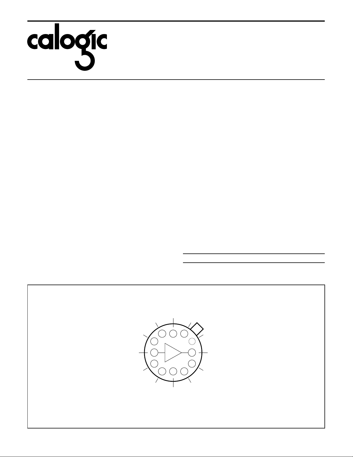
CONNECTION DIAGRAM
LH0033
Metal Can Package
NC
NC
OFFSET
PRESET
OFFSET
ADJUST
Case is electrically Isolated
CALOGIC CORPORATION, 237 Whitney Place, Fremont, California 94 539, Telephone: 5 10-656-2900, FAX: 510-651-1076
NC
4
5
6
789
NC
Top View
Package H12A
+
V
C
123
12
11
10
+
V
OUTPUTINPUT
-
V
V
C
Page 2
LH0033 / LH0033C
CORPORATION
ABSOLUTE MAXIMUM RATINGS
If Military/Aerospace specified devices are required, please
contact Calogic Sales Office for availability and specifications.
+
Supply Voltage (V
- V-). . . . . . . . . . . . . . . . . . . . . . . . . . . 40V
Power Dissipation (See Curve s)
LH0033/LH0033C . . . . . . . . . . . . . . . . . . . . . . . . . . . . 2.2W
Junction Temperature . . . . . . . . . . . . . . . . . . . . . . . . . . 175
Input Voltage . . . . . . . . . . . . . . . . . . . . . . . . . . . . . . . ±V
o
Supply
C
DC ELECTRICAL CHARACTERISTICS: The following specifications apply for supply voltage = ±15V unless otherwise noted (Note 1)
SYMBOL CHARACTERISTICS
V
OS
∆V
OS
∆T
I
B
A
V
R
IN
R
OUT
V
(SWING 1)
V
(SWING 2)
I
S
P
D
Output Offset Voltage
Average Temperature
Coefficient of Offset Voltage
Input Bias Current
Voltage Gain 0.97 0.98 1.00 0.96 0.98 1.00 V/V VO = ±10V, RS = 100Ω, RL = 1.0k Ω
Input Impedance 10
Output Impedance 6.0 10 6.0 10 Ω VIN = ±1.0V, RL = 1.0k
Output Voltage Swing
Supply Current 18 22 18 24 mA VIN = 0V (Note 5)
Power Consumption 540 660 540 720 mW VIN = 0V
LH0033 LH0033C
MIN TYP MAX MIN TYP MAX
5.0 10
15
50 100 50 100 µV/
250
2.5
10
10
10
11
±12 ±12
±9.0 ±9.0 VI = ±10.5V, RL = 100Ω, TA = 25oC
Continuous Output Curr ent
LH0033/LH0033C . . . . . . . . . . . . . . . . . . . . . . . . . ±100mA
Peak Output Current
LH0033/LH0033C . . . . . . . . . . . . . . . . . . . . . . . . . ±250mA
Lead Temp. (Soldering, 10 secon ds). . . . . . . . . . . . . . . 300
Operating Temperatur e Ra nge
LH0033. . . . . . . . . . . . . . . . . . . . . . . . . . . . -55
LH0033C . . . . . . . . . . . . . . . . . . . . . . . . . . . -25
Storage Temperature Ra nge . . . . . . . . . . -65
UNITS CONDITIONS
10
10
12 20
11
10
25
500
5.0
20
mVmVR
pA
nA
nA
= 100Ω, TJ = 25oC,
S
V
= 0V (Note 2), RS = 100Ω
IN
o
CRS = 100Ω, VIN = 0V (Note 3)
V
= 0V
IN
T
= 25oC (Note 2)
J
T
= 25oC (Note 4)
A
T
= TA = T
J
MAX
Ω RL = 1kΩ
V
= ±14V, RL = 1.0k
V
I
o
C to +125oC
o
C to +85oC
o
C to +150oC
o
C
AC ELECTRICAL CHARACTERIST ICS: T
SYMBOL CHARACTERISTICS
= 25oC, VS = ± 15V, RS = 50Ω, RL = 1.0KΩ (Note 3)
J
LH0033 LH0033C
UNITS CONDITIONS
MIN TYP MAX MIN TYP MAX
S
R
BW Bandwidth 100 100 MHz V
Slew Rate 1000 1500 1000 1400 V/µsVIN = ±10V
= 1. 0Vrms
IN
Phase Non- Linearity 2.0 2.0 degrees BW = 1.0Hz to 20MHz
R
T
Rise Time 2.9 3.2 ns ∆VIN = 0.5V
Propagation Delay 1.2 1.5 ns ∆V
= 0.5V
IN
Harmonic Distortion <0.1 <0.1 % f>1kHz
Note 1: LH0033 is 100% production tested as specified at 25
o
C. Specifications at temperature extremes are verified by sample testing,
correlation or periodic characterization.
o
Note 2: Specification is at 25
will exceed the value at T
more under load conditions. Accordingly, V
C junction temperature due to requirements of high speed automatic testing. Actual values at operating temperature
= 25oC. When supply voltages are ±15V, no-load operating junction temperature may rise 40-60oC above ambient, and
J
may change one to several mV, and IB will change significantly during warm-up.
OS
Note 3: Limits are guaranteed by sample testing, periodic characterization or correlation.
Note 4: Mea sured in still air 7 minutes after appli catio n of power. Guaranteed throug h correlated autom at ic pulse testing .
Note 5: Guaranteed through correlated automatic pulse testing at T
= 25oC.
J
CALOGIC CORPORATION, 237 Whitney Place, Fremont, California 94 539, Telephone: 510-656- 2 900, FAX: 510-651-1076
Page 3
CORPORATION
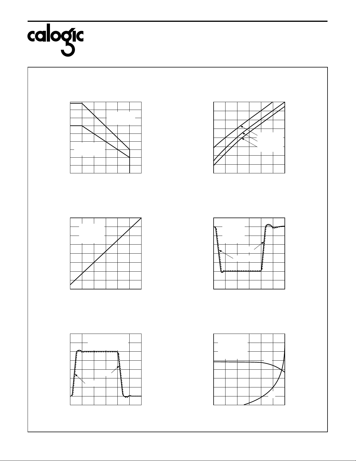
TYPICAL PERFORMANCE CHARACTERI STI CS
LH0033 / LH0033C
POWER DISSIPATION (W)
OUTPUT VOLTAGE (±V)
2.0
1.5
1.0
0.5
0
18
16
14
12
10
8
6
4
POWER DISSIPATION
AMBIENT
θ = 100˚C/W
JA
07525 50
TEMPERATURE (˚C)
OUTPUT VOLTAGE
vs SUPPLY VOLTAGE
RL= 1kΩ
= 100kΩ
R
S
= +25˚C
T
C
CASE
θ = 60˚C/W
JC
100 125 150
SUPPLY CURRENT (±mA)
INPUT/OUTPUT VOLTAGE (-V)
SUPPLY CURRENT
vs SUPPLY VOLTAGE
21
20
19
18
17
5
10
SUPPLY VOLTAGE (±V)
PULSE RESPONSE
V
= ±15V
S
0
-2
-4
-6
-8
-10
-12
R
S
R
L
T
C
= 50Ω
= 1kΩ
= +25˚C
OUTPUT
NEGATIVE
INPUT
TC= +125˚C
= +25˚C
T
C
= -55˚C
T
C
15 20
5
10
SUPPLY VOLTAGE (±V)
15 20
0
10
30 60
20 5040
TIME (ns)
POSITIVE
PULSE RESPONSE
V
= ±15V
S
= 1kΩ,R
12
10
8
6
4
2
INPUT/OUTPUT VOLTAGE (V)
0
030
R
TC= +25˚C
OUTPUT
10 20
L
INPUT
TIME (ns)
= 50Ω
S
40 50 60
VOLTAGE GAIN (V/V)
FREQUENCY RESPONSE
V
= ±15V
S
= 50Ω
R
S
R
= 1kΩ
L
VIN= 1.0 Vrms
1.0
0.8
0.6
0.4
0.2
1.0 10.0
2.0 5.0
FREQUENCY (MHz)
Av
φ
20.0 50 100
40
35
PHASE LAG (DEGREES)
30
25
20
15
10
5
CALOGIC CORPORATION, 237 Whitney Place, Fremont, California 94 539, Telephone: 510-656- 2 900, FAX: 510-651-1076
Page 4

LH0033 / LH0033C
TYPICAL PERFORMANCE CHARACTERI STI CS ( Cont inued )
CORPORATION
RISE AND FALL TIME
8.0
6.0
4.0
2.0
RISE AND FALL TIME (ns)
0
vs TEMPERATURE
V
= ±15V
S
= 50Ω
R
S
RL= 1k
-50
0 50 100
TEMPERATURE (˚C)
NORMALIZED INPUT BIAS
CURRENT DURING WARM-UP
100
VS= ±15V
= 25˚C
T
A
10
INPUT BIAS CURRENT
10
t
f
0.100
t
r
150
0.010
INPUT BIAS CURRENT (nA)
0.001
vs TEMPERATURE
1
VS= ±15V
05025
TEMPERATURE (˚C)
VS= ±10V
VS= ±5V
75 100 125
INPUT BIAS CURRENT
10
1.0
vs INPUT VOLTAGE
VS= ±15V
PULSE TESTED (T
= 25˚C)
J
TO CURRENT AT TIME = 0
CURRENT – NORMALIZED
1
0624
TIME FROM POWER TURN-ON (MINUTES)
810
INPUT BIAS CURRENT (nA)
0.1
10 486
20-2
INPUT VOLTAGE (V)
-6 -10
CALOGIC CORPORATION, 237 Whitney Place, Fremont, California 94 539, Telephone: 510-656- 2 900, FAX: 510-651-1076
Page 5

CORPORATION
APPLICATION INFORMATION:
Recommended Layout Pre caut ions
RF/video printed circuit board layout rules should be followed
when using the LH0033 since it will provide power gain to
frequencies over 100MHz. Ground planes are recommended
and power supplies should be decoupled at each device with
low inductance capacitors. In addition, ground p la ne sh ield ing
may be extended to the metal case of the device since it is
electrically isolated from internal circuitry. Alternatively the
case should be connected to the output to minimize input
capacitance.
LH0033 / LH0033C
where:
AV = No load voltage gain, typically 0.99
+
= Positive supply voltage
V
–
= Negative supply voltage
V
For the above example, ∆V
adjusted to zero as described in Figure 1. For AC coupled
applications, no additional offset occurs if the DC input is
properly biased as illustrated in the Typical Applications
section.
would be -35mV. This may be
O
Offset Voltage Adjust ment
The LH0033’s offset voltages have been actively trimmed by
laser to meet guaranteed specif ications when the off set p re set
pin is shorted to the off set adjust pin. If of fset n u ll is d esir able,
it is simply obtained by leaving the offset preset pin open and
connecting a trim pot of 200Ω for the LH0033 between the
offset adjust pin and V
–
, as illustrated in Figure 1.
Operation From Single Or Asymmetrical Power Supplies
LH0033 may be used in applications where symmetrical
supplies are unavailable or not desirable. A typical application
might be an interface to a MOS shift register where V
–
= -12V. In this case, an apparent output offset occurs
and V
+
= +5V
due to the device’s voltage gain of less than unity. This
additional output error may be pre dict ed by:
+−V−
(V
∆V
≅ (1−AV)
O
)
= 0.005 (V+ −V−)
2
FIGURE 1. Offset Zero Adju st
+15V
1
INPUT
OFFSET
PRESET
(OPEN)
OFFSET
ADJUST
200Ω
5
6
7
LH0033
9
12
10
11
OUTPUT
-15V
Short Circuit Protection
In o rder to o ptimize tra nsient re sponse and o utput swin g,
output current limit has been omitted from the LH0033.
Short circuit protection may be added by inserting
appropriate value resistors between V
–
V
and V
–
pins as il lustrated in Figure 2. Resistor values
C
+
and V
+
pins and
C
may be predi cted by:
+
−
V
R
LIM
≅
V
=
I
I
SC
SC
where:
≤ 100mA for LH0033
I
SC
The inclusion of limiting resistors in the collector s of the output
transistors reduces output voltage swing. Decoupling VC
–
and V
pins with capacitors to ground will retain full output
C
swing for transient pulses. Alternate active current limit
techniques that retain full DC output swing are shown in
FIGURE 2. Resistor Current Limiti ng Usi n g Resistor
+
V
R
LIM
100
INPUT
5
12
LH0033
7
6
1
9
10
R
100
11
LIM
C ≅ 0.1µF
OUTPUT
C ≅ 0.1µF
+
-
V
CALOGIC CORPORATION, 237 Whitney Place, Fremont, California 94 539, Telephone: 510-656- 2 900, FAX: 510-651-1076
Page 6

LH0033 / LH0033C
CORPORATION
Figure 3. In Figure 3, the current sources are saturated
during normal operation, thus apply full supply voltage to the
pins. Under fault conditions, the voltage decreases as
V
C
required by the overload.
For Figure 5:
V
0.6V
LIM
=
BE
=
I
SC
60mA
= 10Ω
R
Capacitive Loading
The LH0033 is designed to drive capacitive loads such as
coaxial cables in excess of several thousand picofarads
without susceptibility to oscillation. However, peak current
resulting from (C × d
) shoul d be limited below absolute
V/dt
maximum pe ak curr ent ratings for the devices.
Thus for the LH0 033:
∆V
IN
(
) × CL ≤ I
∆t
≤ ±250mA
OUT
In addition, power dissipation resulting from driving capacitive
loads plus standby power should be kept below total package
power rating:
pkg. ≥ P
P
D
PDpkg. ≥ (V+–V–) × IS + P
P
≅ (Vp-p)2 × f × C
AC
DC
+ P
AC
AC
L
where:
Vp-p = Peak-to-peak output voltage swing
f = Frequency
= Load Capacitanc e
C
L
Operation Within An Op Am p Loop
LH0033 may be used as a current booster or isolator buffer
within a closed loop with op amps such as LH0032, or
CLM4124. An isolation resistor of 47Ω should be used between
the op amp output and the input of LH0033. The wide bandwidth
and high slew rate of the L H0033 assur e that the loo p has the
characteristics of the op amp and that additional rolloff is not
required.
Hardware
In order to utilize the full drive capabilities of LH0033, it should
be mounted with a heat sink particulary for extended
temperature operation. The case is isolated from the circuit
and may be connect ed to the syst em chassis.
Design Precaution
Power supply bypassing is necessary to prevent oscillation.
Low inductance ceramic disc capacitors with the shortest
practical lead lengths must be connected from each supply
1
lead (within <
⁄4" to 1⁄2" of the device package) to a ground
plane. Capacitors should be one or two 0.1µF in parallel;
adding a 4.7µF solid tantalum capacitor will help t roublsome
instances.
FIGURE 3. Current Limiting Usin g Current Sour ces
12
INPUT
Q1 = Q2 = 2N2905
Q3 = Q4 = 2N2219
LH0033
6
+15V
R
LIM
10
Q2
Q1
1
115
9
10
7
Q3
30k
Q4
R
LIM
10
OUTPUT
0.01µF
-15V
CALOGIC CORPORATION, 237 Whitney Place, Fremont, California 94 539, Telephone: 510-656- 2 900, FAX: 510-651-1076
Page 7

CORPORATION
TYPICAL APPLI CA T IONS
High Input Impedance AC Coupled Ampli fier
+
V
4.7pF
LH0033 / LH0033C
INPUT
0.001µF
+
V
1M
12
5
LH0033
6
0.1µF
CASE
10
7
V
Coaxial Cable Dr iv er
11
9
0.1µF
-
≥
f
100MHz
H
OUTPUT
C1*
43
INPUT
51
5
12
LH0033
1
100
11
9
10
6
100
50Ω
7
-
V
*Select C1 for Optimum Pulse Response
CALOGIC CORPORATION, 237 Whitney Place, Fremont, California 94 539, Telephone: 510-656- 2 900, FAX: 510-651-1076
Page 8

LH0033 / LH0033C
TYPICAL APPLI CA T IONS (Continued)
CORPORATION
High Input Impe dance Comparator with Of f set Adjust
+
V
10
-
+
-
+
5
NO GO = LOGIC "1"
-
V
GO = LOGIC "0"
INPUT
OFFSET
ADJUST
V
U.L.
+
V
12
5
LH0033 LM711
7
1
9
10
-
V
3
4
11
7
6
V
L.L.
Singl e S u pp l y AC Amplifier
INPUT
Instru me nt ation Shiel d/ Line Driver
+
V
12
100
CASE
51
5
LH0033
1
11
9
10
7
100
6
-
V
4.5MHz N ot ch Fi l t er
INPUT
0.001µF
1M
5
V = 12.0V
CC
12
1
LH0033
7
6
10
CASE
9
+
V
12
1
5
LH0033
7
6
11
9
10
-
V
f0=
2π
R1= 2R
C1=
1
R
1C1
2
C
2
2
R2
110
C2
300pF
C1
150pF
Ω
R1
220Ω
C1
150pF
V
11
OUTPUT
IN
R1
220Ω
CALOGIC CORPORATION, 237 Whitney Place, Fremont, California 94 539, Telephone: 510-656- 2 900, FAX: 510-651-1076
Page 9

CORPORATION
TYPICAL APPLI CA T IONS (Continued)
LH0033 / LH0033C
High Speed Sample and Hold
LOGIC
INPUT
ANALOG
INPUT
1
2
5
+
V
7
LH0033
7
+
V
5
12
LH0033
6
7
10
1
11
OUTPUT
9
-
V
TM
100
1
11
9
10
6
100
-
V
100
C1*
1000pF
*Polycarbonate or Teflon
CALOGIC CORPORATION, 237 Whitney Place, Fremont, California 94 539, Telephone: 510-656- 2 900, FAX: 510-651-1076
 Loading...