

Page 1
DISCRETE SEMICONDUCTORS
DATA SH EET
LFE18500X
NPN silicon planar epitaxial
microwave power transistor
Product specification
File under Discrete Semiconductors, SC15
Philips Semiconductors
December 1994
Page 2
Philips Semiconductors Product specification
NPN silicon planar epitaxial
microwave power transistor
FEATURES
• Diffused emitter ballasting resistors
providing excellent current sharing
and withstanding a high VSWR
• Interdigitated structure provides
high emitter efficiency
• Gold metallization realizes very
good stability of the characteristics
and excellent lifetime
• Multicell geometry gives good
balance of dissipated power and
low thermal resistance
• Internal input and output
prematching ensures good stability
and allows an easier design of
wideband circuits.
APPLICATION
Intended for use in common emitter,
class AB amplifiers in CW conditions
for professional applications between
1.8 GHz and 1.9 GHz.
DESCRIPTION
NPN silicon planar epitaxial
microwave power transistor in a
FO-231 glued cap metal ceramic
flange package, with emitter
connected to flange.
QUICK REFERENCE DATA
Microwave performance up to T
=25°C in a common emitter class AB
mb
amplifier.
MODE OF
OPERATIONf(GHz)
Class AB
1.85 24 0.2 ≥48 ≥7 typ. 42 see Figs 7
V
(V)
CE
I
CQ
(A)
(CW)
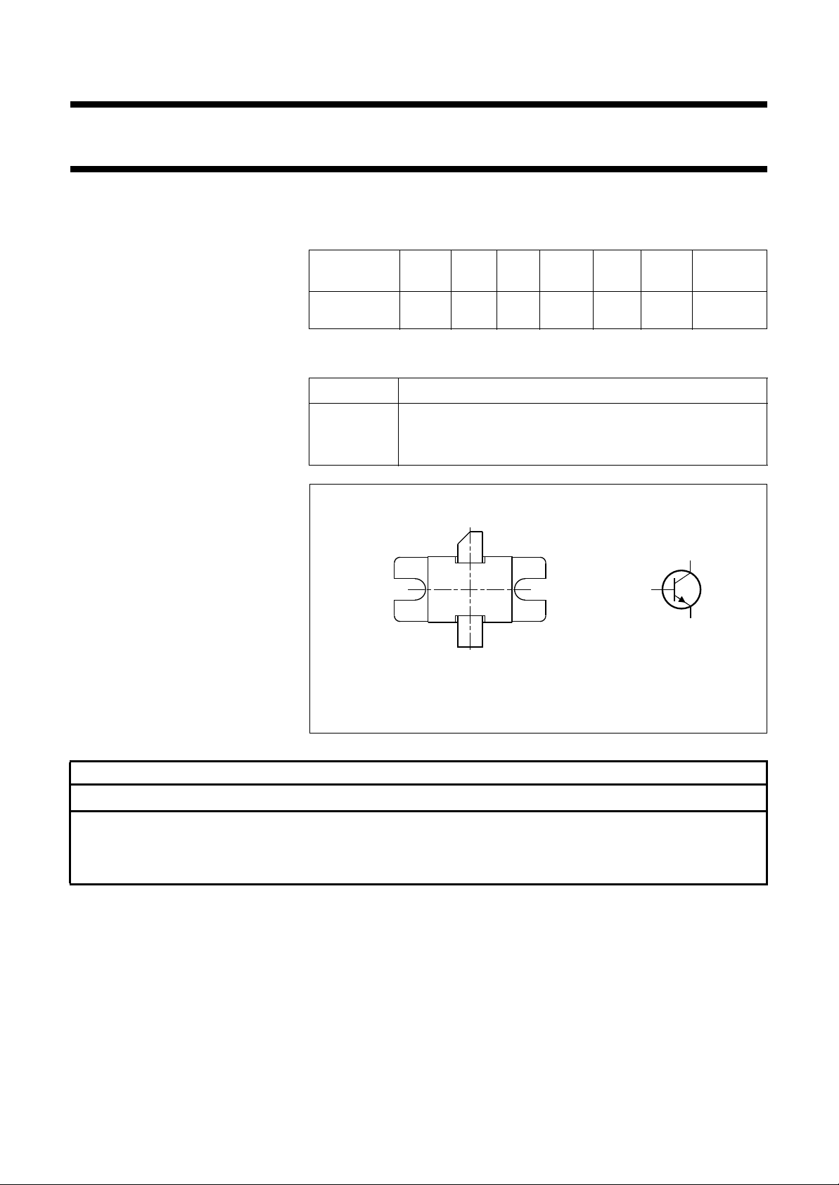
PINNING - FO-231
PIN DESCRIPTION
1 collector
2 base
3 emitter connected to flange
handbook, 4 columns
Top view
1
2
Fig.1 Simplified outline and symbol.
33
P
L1
(W)
G
po
(dB)
MAM045 - 1
LFE18500X
η
C
(%)
b
Zi;Z
(Ω)
and 8
c
e
L
WARNING
Product and environmental safety - toxic materials
This product contains beryllium oxide. The product is entirely safe provided that the BeO slab is not damaged.
All persons who handle, use or dispose of this product should be aware of its nature and of the necessary safety
precautions. After use, dispose of as chemical or special waste according to the regulations applying at the location of
the user. It must never be thrown out with the general or domestic waste.
December 1994 2
Page 3
Philips Semiconductors Product specification
NPN silicon planar epitaxial
LFE18500X
microwave power transistor
LIMITING VALUES
In accordance with the Absolute Maximum Rating System (IEC 134).
SYMBOL PARAMETER CONDITIONS MIN. MAX. UNIT
V
CBO
V
CER
V
CEO
V
EBO
I
C
P
i
P
tot
T
stg
T
j
T
sld
Note
1. Up to 0.2 mm from ceramic.
collector-base voltage open emitter − 45 V
collector-emitter voltage RBE= 220 Ω−30 V
collector-emitter voltage open base − 22 V
emitter-base voltage open collector − 3V
DC collector current − 12 A
input power f = 1.85 GHz; VCE= 24 V; class AB − 20 W
total power dissipation Tmb=75°C − 120 W
storage temperature −65 +200 °C
junction temperature − 200 °C
soldering temperature t ≤ 10 s; note 1 − 235 °C
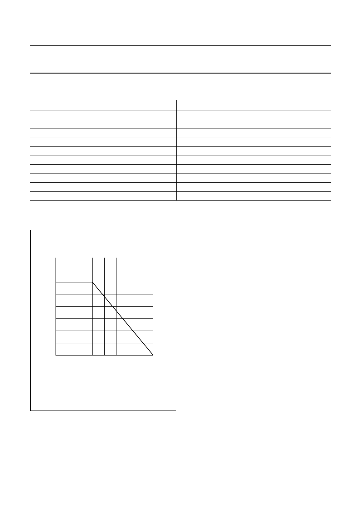
160
handbook, halfpage
P
tot
(W)
120
80
40
0
0 50 100 200
150
T ( C)
Fig.2 Power derating curve.
mb
MLC430
o
December 1994 3
Page 4

Philips Semiconductors Product specification
NPN silicon planar epitaxial
LFE18500X
microwave power transistor
THERMAL CHARACTERISTICS
SYMBOL PARAMETER CONDITIONS MAX. UNIT
R
th j-mb
R
th mb-h
CHARACTERISTICS
=25°C unless otherwise specified.
T
mb
SYMBOL PARAMETER CONDITIONS MIN. MAX. UNIT
I
CBO
V
(BR)CER
V
(BR)CBO
V
(BR)EBO
h
FE
APPLICATION INFORMATION
Microwave performance up to T
thermal resistance from junction to mounting base Tj= 100 °C 1 K/W
thermal resistance from mounting base to heatsink 0.2 K/W
collector cut-off current IE= 0; VCB=20V − 6mA
collector-emitter breakdown voltage IC= 30 mA; RBE=56Ω 30 − V
collector-base breakdown voltage IC=30mA 45 − V
emitter-base breakdown voltage IE=30mA 3 − V
DC current gain IC= 1 A; VCE= 5 V 15 100
=25°C in a common emitter class AB amplifier.
mb
MODE OF
OPERATION
f
(GHz)
V
(V)
CE
I
CQ
(A)
P
L1
(W)
Class AB (CW) 1.85 24 0.2 ≥48
typ. 53
G
po
(dB)
≥7
typ. 7.5
η
(%)
C
Zi; Z
(Ω)
L
typ. 42 see Figs 7
and 8
December 1994 4
Page 5

Philips Semiconductors Product specification
NPN silicon planar epitaxial
microwave power transistor
handbook, full pagewidth
6.0
2.0
5.2
40
2.0
LFE18500X
30
1.5
4.0
4.0
1.5
7.0
2.0
3.0
4.0
3.02.0
5.07.0
3.5
30
15.2
1.0
2.0
40
0.6950.695
1.0
2.0
V
C5
F1
input
C1
The test circuit is split into two independent halves, each being 30 x40 mm in size.
Dimensions in mm.
Substrate: Epsilam 10.
Thickness: 0.635 mm.
Permittivity: εr= 10.
BB
L1
C2
V
C6
L2
C3
CC
C7
output
C4
MLC434
Fig.3 Prematching test circuit board.
December 1994 5
Page 6

Philips Semiconductors Product specification
NPN silicon planar epitaxial
microwave power transistor
handbook, full pagewidth
R1
R2
P1
BIAS CIRCUIT
TR1
D1
D2
LFE18500X
PREMATCHING TEST
CIRCUIT
V
CC
F1
C6
L2
DUT
MEA600
C5
C7R3
L1
Fig.4 Class AB bias circuit.
List of components (see Figs 3 and 4)
COMPONENT DESCRIPTION VALUE ORDERING INFORMATION
TR1 transistor, BDT91 or equivalent
C1, C4 DC blocking chip capacitor 100 pF ATC 100A101kp
C2, C3 trimmer capacitor 0.5 to 5.0 pF Tekelec 727-1
C5, C6 feedthrough bypass capacitor 1500 pF Erie 1250-003
C7 electrolytic capacitor 10 µF, 50 V
D1 diode BY239 or equivalent; note 1
D2 diode BY239 or equivalent; note 2
L1 4 turns 0.5 mm copper wire;
internal diameter = 2 mm
L2 3 turns 0.5 mm copper wire;
internal diameter = 2 mm
P1 linear potentiometer 4.7 kΩ
R1 resistor 100 Ω, 0.25 W
R2 resistor 10 kΩ, 0.25 W
R3 resistor 56 Ω, 0.25 W
F1 ferrite bead Philips tube, 12NC = 4330 030 43081
4.2 x 2.2 x 3.2 mm (4B1)
Notes
1. In thermal contact with TR1.
2. In thermal contact with DUT.
December 1994 6
Page 7

Philips Semiconductors Product specification
NPN silicon planar epitaxial
microwave power transistor
60
handbook, halfpage
P
L
(W)
40
I =
CQ
20
0
04 81216
400 mA
200 mA
100 mA
MLC431
P (W)
i
20
handbook, halfpage
d
im
(dBc)
I =
100 mA
30
200 mA
40
400 mA
50
60
01020 40
CQ
LFE18500X
MLC726
30
P (W)
o (av)
VCE= 24 V; f1= 1849.9 MHz; f2= 1850.1 MHz.
VCE= 24 V; f = 1850 MHz.
Fig.6 Intermodulation distortion as a function
Fig.5 Load power as a function of input power.
Input and optimum load impedances
V
=24V; ICQ= 0.2 A; Zo=10Ω; typical values at PL=PL1 (see Figs 7 and 8).
CE
f
(GHz)
Z
(Ω)
i
1.80 5.0 + j4.9 2.0 − j2.0
1.85 5.5 + j2.0 1.8 − j1.2
1.90 3.7 + j0.6 1.6 − j1.6
of average output power.
Z
(Ω)
L
December 1994 7
Page 8

Philips Semiconductors Product specification
NPN silicon planar epitaxial
microwave power transistor
handbook, full pagewidth
0.2
+ j
0
– j
0.2
VCE= 24 V; Zo=10Ω; ICQ= 0.2 A.
0.5
0.2
0.5
1.9 GHz
Z
1.8 GHz
i
0.5
1
1.85 GHz
1
LFE18500X
2
5
10
1052
∞
10
5
2
MLC432
Fig.7 Input impedance as a function of frequency; typical values at PL=PL1.
handbook, full pagewidth
VCE= 24 V; Zo=10Ω; ICQ= 0.2 A.
1
0.5
0.2
+ j
0
– j
0.2
0.2 0.5 1052
1.85 GHz
Z
L
1.9 GHz
1.8 GHz
0.5
1
2
5
10
∞
10
5
2
MLC433
Fig.8 Optimum load impedance as a function of frequency; typical values at PL=PL1.
December 1994 8
Page 9

Philips Semiconductors Product specification
NPN silicon planar epitaxial
microwave power transistor
PACKAGE OUTLINE
0.15 max
3.3
2.9
3.3
seating plane
15.5 max
26 max
3.7
max
LFE18500X
6
max
1.6 max
3
9.85
max
2.7
min
10.3
10.0
1
Dimensions in mm.
Torque on screws: max. 0.5 Nm.
Recommended screw: M3.
10.15
20.3
Fig.9 FO-231.
33
MSA376
2.7
min
2
December 1994 9
Page 10

Philips Semiconductors Product specification
NPN silicon planar epitaxial
LFE18500X
microwave power transistor
DEFINITIONS
Data Sheet Status
Objective specification This data sheet contains target or goal specifications for product development.
Preliminary specification This data sheet contains preliminary data; supplementary data may be published later.
Product specification This data sheet contains final product specifications.
Limiting values
Limiting values given are in accordance with the Absolute Maximum Rating System (IEC 134). Stress above one or
more of the limiting values may cause permanent damage to the device. These are stress ratings only and operation
of the device at these or at any other conditions above those given in the Characteristics sections of the specification
is not implied. Exposure to limiting values for extended periods may affect device reliability.
Application information
Where application information is given, it is advisory and does not form part of the specification.
LIFE SUPPORT APPLICATIONS
These products are not designed for use in life support appliances, devices, or systems where malfunction of these
products can reasonably be expected to result in personal injury. Philips customers using or selling these products for
use in such applications do so at their own risk and agree to fully indemnify Philips for any damages resulting from such
improper use or sale.
December 1994 10
 Loading...