

Page 1
DEVICES INCORPORATED
LF48410
1024 x 24-bit Video Histogrammer
LF48410
DEVICES INCORPORATED
1024 x 24-bit Video Histogrammer
FEATURES DESCRIPTION
❑❑
❑ 40 MHz Data Input and Compu-
❑❑
tation Rate
❑❑
❑ 1024 x 24-bit Memory Array
❑❑
❑❑
❑ Histograms of Images up to 4K x
❑❑
4K with 10-bit Pixel Resolution
❑❑
❑ Memory Array Flash Clear
❑❑
❑❑
❑ User-Programmable Modes:
❑❑
Histogram, Histogram Accumulate,
Look Up Table, Bin Accumulate,
Delay Memory, Delay and Subtract,
Single Port RAM
❑❑
❑ Replaces Harris HSP48410
❑❑
❑❑
❑ 84-pin PLCC, J-Lead
❑❑
The LF48410 is capable of generating
histograms and Cumulative Distribution Functions of video images. It
may also be used as a look up table, a
bin accumulator, a delay memory
(delay and subtract also possible), or a
single port RAM. The on-chip 1024 x
24-bit memory array facilitates
histograms of images up to 4K x 4K
pixels with a 10-bit pixel resolution.
Once the histogram of a video image
is stored in the memory array, the
Cumulative Distribution Function can
be calculated by putting the device in
Histogram Accumulate Mode.
Transformation functions can be
performed on pixel values when the
device is in Look Up Table Mode. If
the Cumulative Distribution Function
is the desired transformation function, the LF48410 can calculate it and
have it available for Look Up Table
Mode. When the device is in Delay
Memory Mode, it functions as a video
row buffer. In this mode, the LF48410
can buffer video lines as long as 1029
pixels. The device can also function
as an asynchronous single port RAM.
During asynchronous modes, the
device can be configured as a 1024 x
24, 1024 x 16, or 1024 x 8-bit RAM. A
Flash Clear function is provided
which sets all memory array locations
and data path registers to “0”.
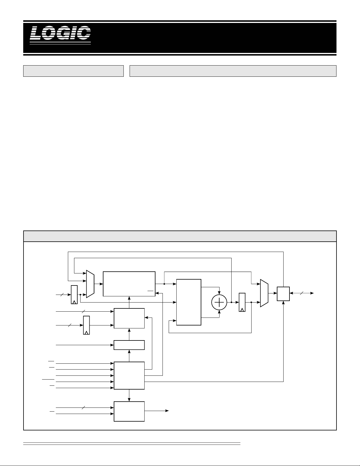
LF48410 BLOCK DIAGRAM
24
DIN
23-0
IOA
9-0
PIN
9-0
CLK
(TO ALL REGISTERS)
WR
RD
UWS
START
FC
FCT
2-0
LD
3
10
10
3
RAM ARRAY
DATA IN DATA OUT
WRADDRESS
ADDRESS
GENERATOR
COUNTER
CONTROL
FUNCTION
DECODE
ADDER
INPUT
CONTROL
MUX CONTROL SIGNALS
DIO
I/F
24
DIO
23-0
Video Imaging Products
1
08/08/2000–LDS.48410-L
Page 2
DEVICES INCORPORATED
LF48410
1024 x 24-bit Video Histogrammer
SIGNAL DEFINITIONS
Power
VCC and GND
+5 V power supply. All pins must be
connected.
Clock
CLK — Master Clock
When operating in a synchronous
mode, the rising edge of CLK strobes
all enabled registers. CLK has no
effect when operating in an asynchronous mode.
Inputs
PIN9-0 — Pixel Data Input
PIN9-0 provides address information
to the memory array in Histogram,
Bin Accumulate, and Look Up Table
Modes. Data is latched on the rising
edge of CLK.
DIN23-0 — Data Input
In Bin Accumulate Mode, DIN23-0
provides data to the internal summer
to be added to data already in the
memory array. In Look Up Table
Mode, DIN23-0 is used to load the
memory array with the desired
values. In Delay Memory Mode, the
data to be delayed is input to the
memory array using DIN23-0, and in
Delay and Subtract Mode it also
provides data to be subtracted from
the delayed data. In all four modes,
DIN23-0 is latched on the rising edge
of CLK.
IOA9-0 — Asynchronous Address Input
IOA9-0 provides address information
to the memory array in Asynchronous
16 and 24 Modes.
FCT2-0 — Function Input
FCT2-0 is used to put the LF48410 into
one of its eight modes of operation
(Table 1). Data is latched on the
rising edge of LD. To ensure proper
operation of the device, START must
be HIGH while changing modes, and
there must be at least one rising edge
of CLK between the rising edge of LD
and the falling edge of START.
Inputs/Outputs
DIO23-0 — Data Input/Output
In all synchronous modes, DIO23-0 is
the 24-bit registered data output port.
In all asynchronous modes, DIO23-0 is
both the data input and data output
port for the memory array.
Controls
START — Device Enable
START is used to enable and disable
the synchronous modes of operation
(except for the Delay Memory and
Delay and Subtract Modes). The
synchronous mode sections explain
how START functions in each mode.
START has no effect in asynchronous
modes. Data is latched on the rising
edge of CLK. START must be held
HIGH when changing from one mode
to another. To ensure proper operation of the device, there must be at
least one rising edge of CLK between
the rising edge of LD and the falling
edge of START.
RD — Read/Output Enable
In all synchronous modes, RD is used
as an output enable for DIO23-0.
When RD is LOW, DIO23-0 is enabled
for output. When RD is HIGH, DIO23-0
is placed in a high-impedance state.
In all asynchronous modes, RD is
used as a read enable for the memory
array (see asynchronous mode
sections for details).
WR — Write Enable
In all asynchronous modes, WR is
used as a write enable for the
memory array (see asynchronous
mode sections for details). WR has
no effect in the synchronous modes.
UWS — Upper Word Select
UWS is only used in Asynchronous 16
Mode. If UWS is LOW and a memory
write is performed, data on DIO15-0 is
written to the lower 16 bits of the
addressed 24-bit word. If UWS is
LOW and a memory read is performed, the lower 16 bits of the
addressed 24-bit word will be output
on DIO15-0. If UWS is HIGH and a
memory write is performed, data on
DIO7-0 is written to the upper 8 bits of
the addressed 24-bit word. If UWS is
HIGH and a memory read is performed, the upper 8 bits of the
addressed 24-bit word will be output
on DIO7-0.
FC — Flash Clear
When FC is LOW, all memory array
locations and data path registers are
set to “0”. To ensure that Flash Clear
functions properly, FC should not be
set LOW until START is HIGH
(synchronous modes) or WR is HIGH
(asynchronous modes).
LD — Function Load Strobe
Data present on FCT2-0 is latched into
the LF48410 on the rising edge of LD.
To ensure proper operation of the
device, there must be at least one
rising edge of CLK between the rising
edge of LD and the falling edge of
START.
TABLE 1. LF48410 MODES
FCT2-0 MODE
0 0 0 Histogram
0 0 1 Histogram Accumulate
0 1 0 Delay and Subtract
0 1 1 Look Up Table
1 0 0 Bin Accumulate
1 0 1 Delay Memory
1 1 0 Asynchronous 24
1 1 1 Asynchronous 16
Video Imaging Products
2
08/08/2000–LDS.48410-L
Page 3
DEVICES INCORPORATED
LF48410
1024 x 24-bit Video Histogrammer
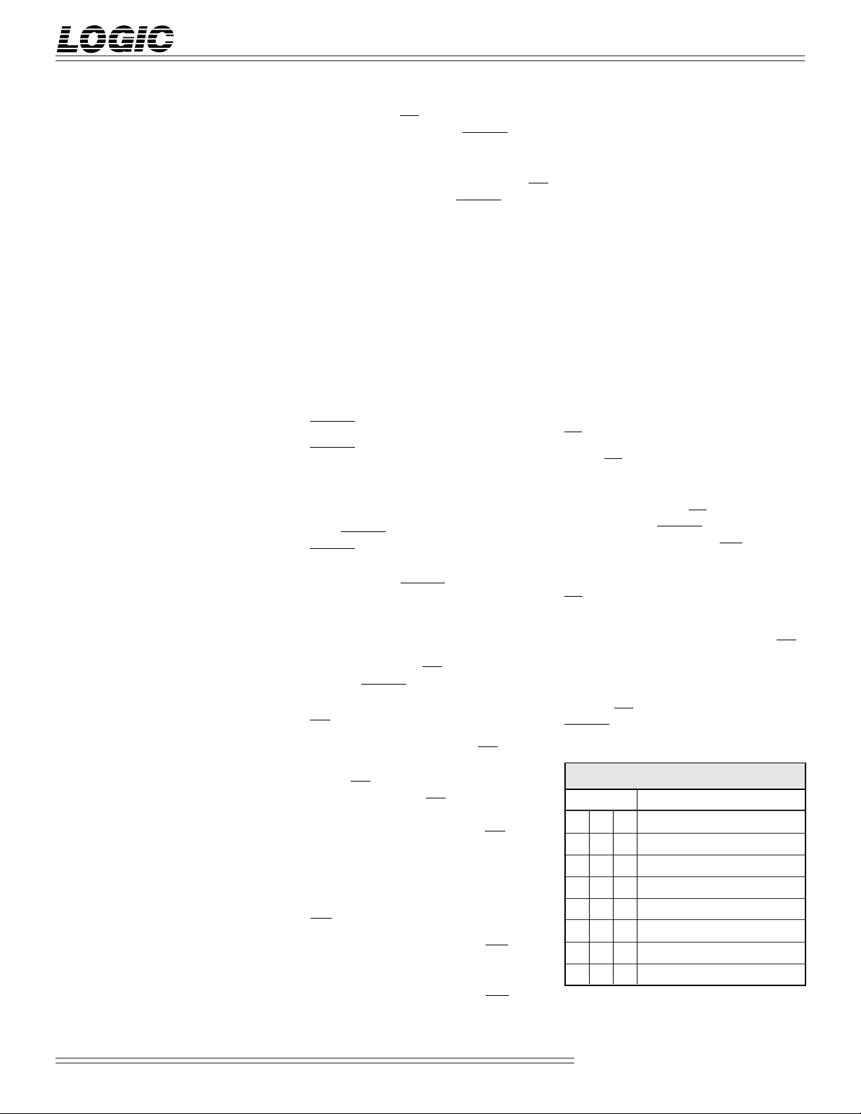
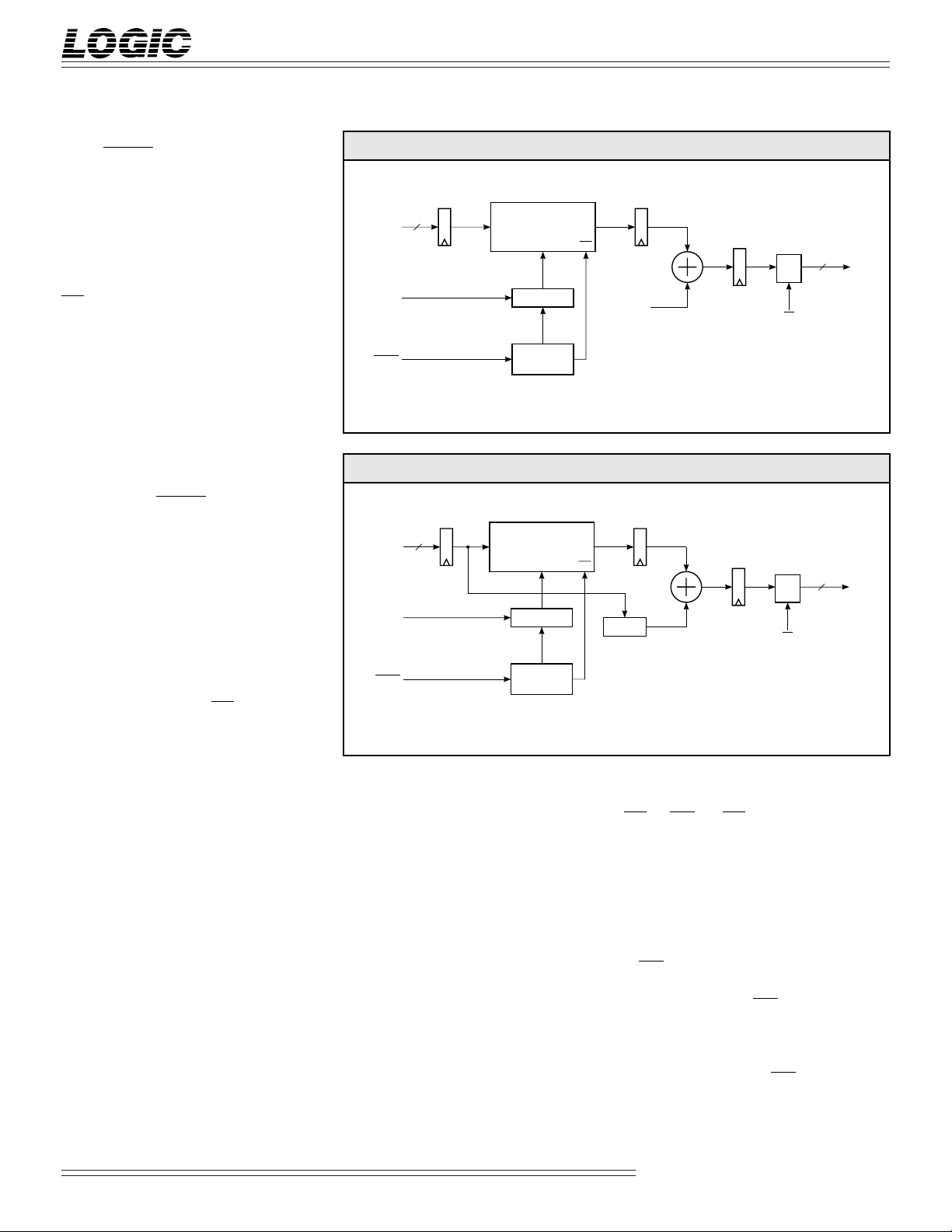
HISTOGRAM MODE
When the LF48410 is in this mode, the
chip is configured as shown in Figure
1. The memory array keeps track of
how many times a particular pixel
value is used in a video image. The
pixel value is input on PIN9-0 and is
latched on the rising edge of CLK.
Data at the address defined by PIN9-0
is read out of the memory array and
incremented by one. The data is then
written back to the memory array, in
the same location it was read from,
and is also output on DIO23-0 (if RD is
LOW). As long as START is LOW,
the device will be enabled for Histogram Mode. When START is HIGH,
the device will still read pixel values,
but the addres-sed data will not be
incremented. The unchanged data is
output on DIO23-0 and is not written
back to the memory array (writing is
disabled). START is delayed internally three clock cycles to match the
latency of the address generator.
HISTOGRAM ACCUMULATE
MODE
When the LF48410 is in this mode, the
chip is configured as shown in Figure
2. This mode is used to calculate the
Cumulative Distribution Function of
a video image. Before this can be
done, the histogram of the image
must already be in the memory array.
The internal counter is used to
generate address data for the memory
array. Data at the address defined by
the counter is read out of the memory
array and added to the sum of the
data from all previous address
locations. This new value is written
back to the memory array, in the
same location where the last read
occurred, and is also output on
DIO23-0 (if RD is LOW). After all
memory locations with histogram
data are accumulated, the memory
array will contain the Cumulative
Distribution Function.
After this mode is selected, the
internal counter and all data path
registers are reset to zero when
FIGURE 1. HISTOGRAM MODE
RAM ARRAY
DATA IN DATA OUT
WRADDRESS
10
PIN
9-0
START
CLK TO ALL REGISTERS
ADDRESS
GENERATOR
CONTROL
"0"
"1"
FIGURE 2. HISTOGRAM ACCUMULATE MODE
RAM ARRAY
DATA IN DATA OUT
ADDRESS
ADDRESS
GENERATOR
(TO ALL REGISTERS)
START
COUNTERCLK
CONTROL
START is set LOW. Every rising edge
of CLK causes the counter to increment its output by one until the
counter reaches a value of 1023. At
this point, the counter will hold the
value of 1023 and writing to the
memory array will be disabled. As
long as START is LOW, the device
will be enabled for Histogram Accumulate Mode. When START is HIGH,
the counter will still increment its
address values, but the addressed
data will not be added to anything.
The unchanged data is output on
DIO23-0 and is not written back to the
memory array (writing is disabled).
START is delayed internally three
clock cycles to match the latency of
the address generator.
WR
"0"
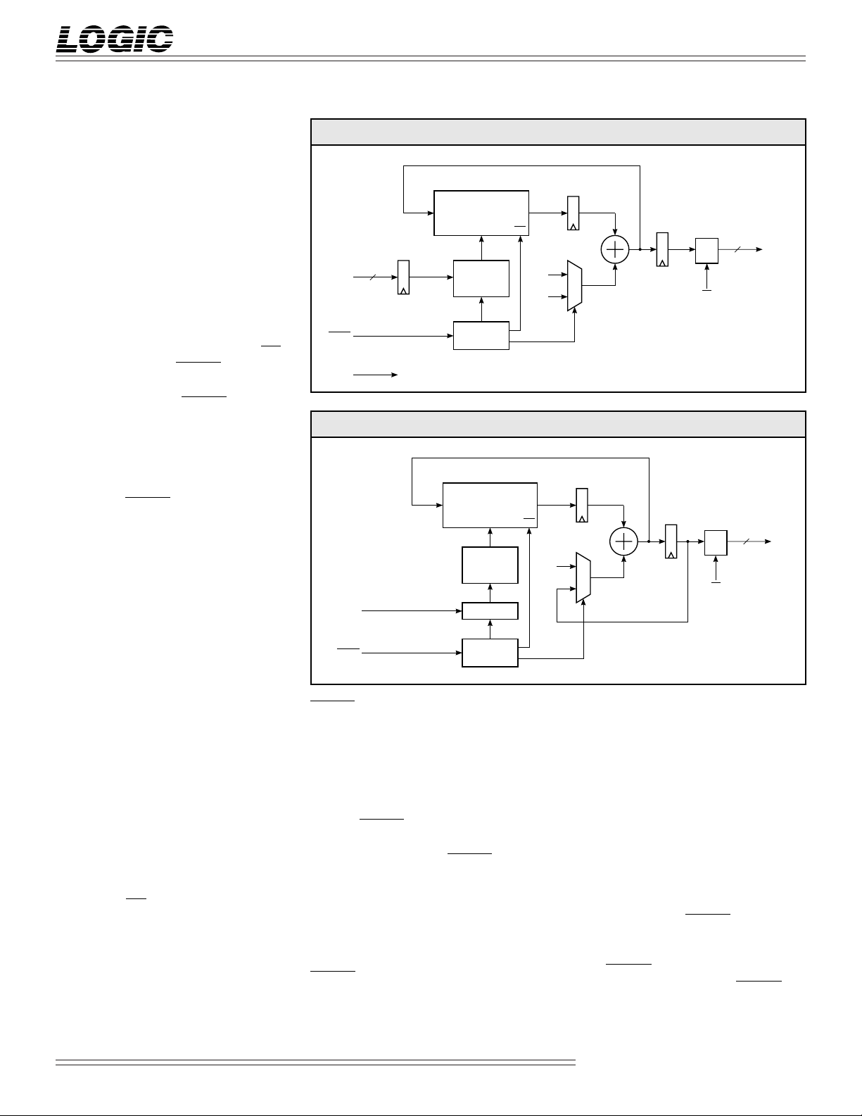
LOOK UP TABLE MODE
When the LF48410 is in this mode, the
chip is configured as shown in Figure
3. This mode is used to perform fixed
transformation functions on pixel
values. The transformation function
can be loaded into the memory array
in Look Up Table Write Mode,
Asynchronous 16/24 Mode, or
Histogram Accumulate Mode. In
Look Up Table Write Mode, data is
loaded into the memory array using
DIN23-0, CLK, and START. The
internal counter is used to generate
address data for the memory array.
When START goes LOW, the counter
is reset to zero. As long as START is
LOW, data on DIN23-0 is latched on
the rising edge of CLK and loaded
DIO
I/F
RD
DIO
I/F
RD
24
DIO
23-0
24
DIO
23-0
Video Imaging Products
3
08/08/2000–LDS.48410-L
Page 4
DEVICES INCORPORATED
LF48410
1024 x 24-bit Video Histogrammer
FIGURE 3. LOOK UP TABLE MODE
24
DIN
23-0
10
PIN
9-0
CLK
(TO ALL REGISTERS)
START
3
RAM ARRAY
DATA IN DATA OUT
WRADDRESS
ADDRESS
GENERATOR
COUNTER
CONTROL
FIGURE 4. BIN ACCUMULATE MODE
RAM ARRAY
DATA IN DATA OUT
ADDRESS
24
DIN
23-0
PIN
9-0
START
CLK TO ALL REGISTERS
3
10
ADDRESS
GENERATOR
CONTROL
into the memory array at the address
defined by the counter. The value
already in the memory array at that
address is output on DIO23-0 (if RD is
LOW). Every rising edge of CLK
causes the counter to increment its
output by one until the counter
reaches a value of 1023. At this point,
the counter will hold the value of
1023 and writing to the memory array
will be disabled. DIN23-0 is delayed
internally three clock cycles to match
the latency of the address generator.
In Asynchronous 16/24 Mode, data is
loaded into the memory array as
detailed in the asynchronous mode
WR
"0"
24
DIO
I/F
"0"
NOTE: NUMBER IN REGISTER INDICATES
NOTE: NUMBER IN REGISTER INDICATES
RD
NUMBER OF PIPELINE DELAYS.
DIO
I/F
RD
NUMBER OF PIPELINE DELAYS.
DIO
23-0
24
DIO
23-0
sections. If the Cumulative Distribution Function is the desired transformation function, the memory array
will contain this data as soon as the
Histogram Accumulate function has
been completed.
Once the memory array contains the
desired data, the device needs to be
put in Look Up Table Read Mode by
setting START HIGH. In Look Up
Table Read Mode, pixel values are
input on PIN9-0 and are latched on
the rising edge of CLK. Data at the
address defined by PIN9-0 is read out
of the memory array and output on
DIO23-0 (if RD is LOW). If Look Up
Table Write Mode was used to load
the memory array, it is important to
wait until the third clock cycle after
START goes HIGH to input data on
PIN9-0 to insure that all data is
written into the memory array before
any reading is done.
BIN ACCUMULATE MODE
When the LF48410 is in this mode, the
chip is configured as shown in Figure
4. PIN9-0 provides address data for
the memory array and is latched on
the rising edge of CLK. Data at the
address defined by PIN9-0 is read out
of the memory array and added to
the data on DIN23-0. This new value
is written back to the memory array,
in the same location where the last
read occured, and is also output on
DIO23-0 (if RD is LOW). As long as
START is LOW, the device will be
enabled for Bin Accumulate Mode.
When START is HIGH, the device will
still read address values on PIN9-0, but
the addressed data will not be added
to anything. The unchanged data will
be output on DIO23-0 and is not
written back to the memory array
(writing is disabled). START and
DIN23-0 are delayed internally three
clock cycles to match the latency of
the address generator.
DELAY MEMORY MODE
When the LF48410 is in this mode, the
chip is configured as shown in Figure
5. This mode allows the device to
function as a row buffer. The internal
counter is used to generate address
data for the memory array. When
START goes LOW, the counter is
reset to zero. Delay length (row
length) is determined by reseting the
counter every N–4 clock cycles, where
N is the number of delays. For
Video Imaging Products
4
08/08/2000–LDS.48410-L
Page 5
DEVICES INCORPORATED
LF48410
1024 x 24-bit Video Histogrammer
example, to set the number of delays
to 10, START would have to be set
LOW every 6 cycles. The maximum
delay length is 1029 and the minimum
delay length is 6. Data on DIN23-0
is latched on the rising edge of
CLK and loaded into the memory
array at the address defined by the
counter. Data is output on DIO23-0 (if
RD is LOW). If the counter reaches
the value of 1023, the counter will
hold this value and writing to the
memory array will be disabled.
DELAY AND SUBTRACT MODE
When the LF48410 is in this mode, the
chip is configured as shown in Figure 6.
The internal counter is used to generate address data for the memory
array. When START goes LOW, the
counter is reset to zero. Delay length
(row length) is determined by
reseting the counter every N–4 clock
cycles, where N is the number of
delays. The maximum delay length is
1029 and the minimum delay length
is 6. Data on DIN23-0 is latched on the
rising edge of CLK and loaded into
the memory array at the address
defined by the counter. Data is
output on DIO23-0 (if RD is LOW).
Before data read from the memory
array is output to DIO23-0, input data
is subtracted from it according to the
following formula: OUTC = D(C–N+1) –
D(C–3). OUTC is the data sent to the
output port (DIO23-0) on clock cycle C.
D(C–N+1) is the data latched into the
device on clock cycle C–N+1, and D(C-
3) is the data latched into the device on
clock cycle C–3. N is the number of
delays. For example, to determine
what will be output on DIO23-0 on
clock cycle 12 when the device is set
for 10 delays, set C=12 and N=10 to
obtain: OUT12 = D3 – D9. If the
counter reaches the value of 1023, the
counter will hold this value and
writing to the memory array will be
disabled.
FIGURE 5. DELAY MEMORY MODE
24
DIN
23-0
CLK COUNTER
(TO ALL REGISTERS)
START
3
RAM ARRAY
DATA IN DATA OUT
ADDRESS
CONTROL
WR
FIGURE 6. DELAY AND SUBTRACT MODE
24
DIN
23-0
CLK COUNTER
(TO ALL REGISTERS)
START
3
ASYNCHRONOUS 16 MODE
When the LF48410 is in this mode, the
chip is configured as shown in Figure 7.
This mode allows the device to
function as an asynchronous single
port RAM. Each 24-bit memory
location is split into two parts, the
lower 16 bits and the upper 8 bits.
IOA9-0 addresses the 24-bit memory
locations, and UWS addresses the
lower 16 or upper 8 bits of those
locations. If UWS is LOW, the lower
16 bits of the 24-bit memory location
are addressed. If UWS is HIGH, the
upper 8 bits are addressed. Address
RAM ARRAY
DATA IN DATA OUT
ADDRESS
CONTROL
WR
–DIN
23-0
data on IOA9-0 and UWS is latched
into the device on the falling edge of
RD or WR. If RD latches the address
data, a memory read is performed.
Data at the specified address is
output on DIO15-0 (if UWS was
latched LOW) or DIO7-0 (if UWS was
latched HIGH). If UWS was latched
LOW/HIGH, DIO16-23/DIO8-23 will
output zeros during a memory read.
If WR latches the address data, a
memory write is performed. After
the falling edge of WR latches the
address, data on DIO15-0 (if UWS was
latched LOW) or DIO7-0 (if UWS was
latched HIGH) is written to the RAM
on the rising edge of WR.
24
DIO
I/F
"0"
NOTE: NUMBER IN REGISTER INDICATES
NOTE: NUMBER IN REGISTER INDICATES
RD
NUMBER OF PIPELINE DELAYS.
DIO
I/F
RD
NUMBER OF PIPELINE DELAYS.
DIO
23-0
24
DIO
23-0
Video Imaging Products
5
08/08/2000–LDS.48410-L
Page 6

DEVICES INCORPORATED
LF48410
1024 x 24-bit Video Histogrammer
ASYNCHRONOUS 24 MODE
When the LF48410 is in this mode, the
chip is configured as shown in Figure 7.
In this mode, the device functions the
same as when in Asynchronous 16
Mode except that the 24-bit memory
locations are not split into two parts.
All 24 bits are used during a read or
write operation. When reading, data
is output on DIO23-0. When writing,
data is input on DIO23-0. UWS is not
used in this mode.
FIGURE 7. ASYNCHRONOUS 16/24 MODE
RAM ARRAY
DATA IN DATA OUT
WRADDRESS
IOA
UWS
9-0
WR
RD
10
ADDRESS
GENERATOR
CONTROL
DIO
I/F
24
DIO
23-0
Video Imaging Products
6
08/08/2000–LDS.48410-L
Page 7

DEVICES INCORPORATED
LF48410
1024 x 24-bit Video Histogrammer
MAXIMUM RATINGS
Storage temperature ........................................................................................................... –65°C to +150°C
Operating ambient temperature........................................................................................... –55°C to +125°C
VCC supply voltage with respect to ground............................................................................ –0.5 V to +7.0V
Input signal with respect to ground ............................................................................... –0.5 V to VCC + 0.5 V
Signal applied to high impedance output ...................................................................... –0.5 V to VCC + 0.5 V
Output current into low outputs............................................................................................................. 25 mA
Latchup current ............................................................................................................................... > 400 mA
OPERATING CONDITIONS
Active Operation, Commercial 0°C to +70°C 4.75 V ≤ VCC ≤ 5.25 V
Active Operation, Military –55°C to +125°C 4.50 V ≤ VCC ≤ 5.50 V
ELECTRICAL CHARACTERISTICS
Above which useful life may be impaired (Notes 1, 2, 3, 8)
To meet specified electrical and switching characteristics
Mode Temperature Range (Ambient) Supply Voltage
Over Operating Conditions (Note 4)
Symbol Parameter Test Condition Min Typ Max Unit
VOH Output High Voltage VCC = Min., IOH = –2.0 mA 2.6 V
VOL Output Low Voltage VCC = Min., IOL = 4.0 mA 0.4 V
VIH Input High Voltage 2.2 VCC V
VIL Input Low Voltage (Note 3) 0.0 0.8 V
IIX Input Current Ground ≤ VIN ≤ VCC (Note 12) ±10 µA
IOZ Output Leakage Current Ground ≤ VOUT ≤ VCC (Note 12) ±10 µA
ICC1 VCC Current, Dynamic (Notes 5, 6) 310 mA
ICC2 VCC Current, Quiescent (Note 7) 500 µA
CIN Input Capacitance TA = 25°C, f = 1 MHz 12 pF
COUT Output Capacitance TA = 25°C, f = 1 MHz 12 pF
Video Imaging Products
7
08/08/2000–LDS.48410-L
Page 8

DEVICES INCORPORATED
6
6
6
6
6
6
6
6
6
6
6
6
6
6
6
6
6
6
6
6
6
6
6
6
6
6
6
6
6
6
6
6
6
6
6
6
6
6
6
6
6
6
6
6
6
6
6
6
6
6
6
6
6
6
6
6
6
6
6
6
6
6
6
6
6
6
6
6
6
6
6
6
6
6
6
6
6
6
6
6
6
6
6
6
6
6
6
6
6
6
6
6
6
6
4
4
SWITCHING CHARACTERISTICS
LF48410
1024 x 24-bit Video Histogrammer
COMMERCIAL OPERATING RANGE (0°C to +70°C)
Symbol Parameter Min Max Min Max Min Max
tCYC Cycle Time 30 25 15
tPWL Clock Pulse Width Low 12 10 10
tPWH Clock Pulse Width High 12 10 10
tPS PIN9-0 Setup Time 13 12 5
tPH PIN9-0 Hold Time 2 2 2
tDS DIN23-0 Setup Time 13 12 5
tDH DIN23-0 Hold Time 2 2 2
tSS START Setup Time 13 12 5
tSH START Hold Time 2 2 2
tCY Read/Write Cycle Time 65 55 35
tAS Address Setup Time 15 13 5
tAH Address Hold Time 2 2 2
tWL WR Pulse Width Low 15 12 7
tWH WR Pulse Width High 15 12 5
tWDS DIO23-0 Setup Time 15 12 5
tWDH DIO23-0 Hold Time 2 2 2
tRL RD Pulse Width Low 43 35 25
tRH RD Pulse Width High 17 15 8
tRD RD Low to DIO23-0 Valid 43 35 25
tOH RD High to DIO23-0 Valid 0 0 0
tLL LD Pulse Width 12 10 7
tLS LD Setup to START 3 0 25 15
tFS FCT2-0 Setup Time 10 10 5
tFH FCT2-0 Hold Time 2 2 2
tFL FC Pulse Width 35 35 15
tD Output Delay 19 15 11
tENA Three-State Output Enable Delay (Note 11) 19 18 15
tDIS Three-State Output Disable Delay (Note 11) 19 18 15
2345678901234567890123
2345678901234567890123
*DISCONTINUED SPEED GRADE
Notes 9, 10 (ns)
8
LF48410–
30 25 15
23456789012345
23456789012345
23456789012345
23456789012345
23456789012345
23456789012345
23456789012345
23456789012345
23456789012345
23456789012345
23456789012345
23456789012345
23456789012345
23456789012345
23456789012345
23456789012345
23456789012345
23456789012345
23456789012345
23456789012345
23456789012345
23456789012345
23456789012345
23456789012345
23456789012345
23456789012345
23456789012345
23456789012345
23456789012345
23456789012345
23456789012345
23456789012345
23456789012345
23456789012345
23456789012345
23456789012345
23456789012345
23456789012345
23456789012345
23456789012345
23456789012345
23456789012345
23456789012345
23456789012345
23456789012345
23456789012345
23456789012345
23456789012345
23456789012345
23456789012345
23456789012345
23456789012345
23456789012345
23456789012345
23456789012345
23456789012345
23456789012345
23456789012345
23456789012345
23456789012345
23456789012345
23456789012345
23456789012345
23456789012345
23456789012345
23456789012345
23456789012345
23456789012345
23456789012345
23456789012345
23456789012345
23456789012345
23456789012345
23456789012345
23456789012345
23456789012345
23456789012345
23456789012345
23456789012345
23456789012345
23456789012345
23456789012345
23456789012345
23456789012345
23456789012345
23456789012345
23456789012345
23456789012345
23456789012345
23456789012345
23456789012345
23456789012345
23456789012345
23456789012345
Video Imaging Products
08/08/2000–LDS.48410-L
*
Page 9

DEVICES INCORPORATED
4
4
4
4
4
4
4
4
4
4
4
4
4
4
4
4
4
4
4
4
4
4
4
4
4
4
4
4
4
4
4
4
4
4
4
4
4
4
4
4
4
4
4
4
4
4
4
4
4
4
4
4
4
4
4
4
4
4
4
4
4
4
4
4
4
4
4
4
4
4
4
4
4
4
4
4
4
4
4
4
4
4
4
4
4
4
4
4
4
4
4
4
4
4
4
4
SWITCHING CHARACTERISTICS
LF48410
1024 x 24-bit Video Histogrammer
MILITARY OPERATING RANGE (–55°C to +125°C)
Symbol Parameter Min Max Min Max Min Max
tCYC Cycle Time 39 30 25
tPWL Clock Pulse Width Low 15 12 12
tPWH Clock Pulse Width High 15 12 12
tPS PIN9-0 Setup Time 16 15 12
tPH PIN9-0 Hold Time 2 2 2
tDS DIN23-0 Setup Time 16 15 12
tDH DIN23-0 Hold Time 2 2 2
tSS START Setup Time 16 15 12
tSH START Hold Time 2 2 2
tCY Read/Write Cycle Time 80 65 55
tAS Address Setup Time 20 16 13
tAH Address Hold Time 2 2 2
tWL WR Pulse Width Low 20 15 12
tWH WR Pulse Width High 20 15 10
tWDS DIO23-0 Setup Time 20 16 12
tWDH DIO23-0 Hold Time 2 2 2
tRL RD Pulse Width Low 55 43 35
tRH RD Pulse Width High 20 17 15
tRD RD Low to DIO23-0 Valid 55 43 35
tOH RD High to DIO23-0 High Z 0 0 0
tLL LD Pulse Width 15 12 10
tLS LD Setup to START 3 9 30 25
tFS FCT2-0 Setup Time 15 12 10
tFH FCT2-0 Hold Time 2 2 2
tFL FC Pulse Width 35 35 35
tD Output Delay 24 19 15
tENA Three-State Output Enable Delay (Note 11) 24 19 18
tDIS Three-State Output Disable Delay (Note 11) 27 27 18
2345678901234567890123
2345678901234567890123
*DISCONTINUED SPEED GRADE
Notes 9, 10 (ns)
23456789012345678901234567890121234567890123
23456789012345678901234567890121234567890123
23456789012345678901234567890121234567890123
23456789012345678901234567890121234567890123
23456789012345678901234567890121234567890123
23456789012345678901234567890121234567890123
23456789012345678901234567890121234567890123
23456789012345678901234567890121234567890123
23456789012345678901234567890121234567890123
23456789012345678901234567890121234567890123
23456789012345678901234567890121234567890123
23456789012345678901234567890121234567890123
23456789012345678901234567890121234567890123
23456789012345678901234567890121234567890123
23456789012345678901234567890121234567890123
23456789012345678901234567890121234567890123
23456789012345678901234567890121234567890123
23456789012345678901234567890121234567890123
23456789012345678901234567890121234567890123
23456789012345678901234567890121234567890123
23456789012345678901234567890121234567890123
23456789012345678901234567890121234567890123
23456789012345678901234567890121234567890123
23456789012345678901234567890121234567890123
23456789012345678901234567890121234567890123
23456789012345678901234567890121234567890123
23456789012345678901234567890121234567890123
23456789012345678901234567890121234567890123
23456789012345678901234567890121234567890123
23456789012345678901234567890121234567890123
23456789012345678901234567890121234567890123
23456789012345678901234567890121234567890123
23456789012345678901234567890121234567890123
23456789012345678901234567890121234567890123
23456789012345678901234567890121234567890123
23456789012345678901234567890121234567890123
23456789012345678901234567890121234567890123
23456789012345678901234567890121234567890123
23456789012345678901234567890121234567890123
23456789012345678901234567890121234567890123
23456789012345678901234567890121234567890123
23456789012345678901234567890121234567890123
23456789012345678901234567890121234567890123
23456789012345678901234567890121234567890123
23456789012345678901234567890121234567890123
23456789012345678901234567890121234567890123
23456789012345678901234567890121234567890123
23456789012345678901234567890121234567890123
23456789012345678901234567890121234567890123
23456789012345678901234567890121234567890123
23456789012345678901234567890121234567890123
23456789012345678901234567890121234567890123
23456789012345678901234567890121234567890123
23456789012345678901234567890121234567890123
23456789012345678901234567890121234567890123
23456789012345678901234567890121234567890123
23456789012345678901234567890121234567890123
23456789012345678901234567890121234567890123
23456789012345678901234567890121234567890123
23456789012345678901234567890121234567890123
23456789012345678901234567890121234567890123
23456789012345678901234567890121234567890123
23456789012345678901234567890121234567890123
23456789012345678901234567890121234567890123
23456789012345678901234567890121234567890123
23456789012345678901234567890121234567890123
23456789012345678901234567890121234567890123
23456789012345678901234567890121234567890123
23456789012345678901234567890121234567890123
23456789012345678901234567890121234567890123
23456789012345678901234567890121234567890123
23456789012345678901234567890121234567890123
23456789012345678901234567890121234567890123
23456789012345678901234567890121234567890123
23456789012345678901234567890121234567890123
23456789012345678901234567890121234567890123
23456789012345678901234567890121234567890123
23456789012345678901234567890121234567890123
23456789012345678901234567890121234567890123
23456789012345678901234567890121234567890123
23456789012345678901234567890121234567890123
23456789012345678901234567890121234567890123
23456789012345678901234567890121234567890123
23456789012345678901234567890121234567890123
23456789012345678901234567890121234567890123
23456789012345678901234567890121234567890123
23456789012345678901234567890121234567890123
23456789012345678901234567890121234567890123
23456789012345678901234567890121234567890123
23456789012345678901234567890121234567890123
23456789012345678901234567890121234567890123
23456789012345678901234567890121234567890123
23456789012345678901234567890121234567890123
23456789012345678901234567890121234567890123
9
39
LF48410–
*
30
*
25
*
Video Imaging Products
08/08/2000–LDS.48410-L
Page 10

DEVICES INCORPORATED
SWITCHING WAVEFORMS:HISTOGRAM MODE
1234567
CLK
t
t
SS
t
SH
SS
START
t
PIN
9-0
t
PH
PS
1234 567
t
SH
RD
t
DIO
23-0
DIS
HIGH IMPEDANCE
t
ENA
*RAM contents not changed.
SWITCHING WAVEFORMS:HISTOGRAM ACCUMULATE MODE
LF48410
1024 x 24-bit Video Histogrammer
t
t
t
D
PWH
PWL
t
CYC
123*
1234567
CLK
t
t
SS
t
SH
SS
START
RD
t
DIO
23-0
DIS
HIGH IMPEDANCE
t
ENA
*RAM contents not changed.
SWITCHING WAVEFORMS:BIN ACCUMULATE MODE
1234567
CLK
t
SH
SS
START
9-0
PIN
23-0
DIN
t
SS
t
t
t
PH
PS
1 234 567
t
DH
DS
1 234 567
t
t
t
t
SH
t
D
t
t
SH
PWH
PWL
t
CYC
123*
t
PWH
PWL
t
CYC
DIO
RD
23-0
*RAM contents not changed.
t
DIS
HIGH IMPEDANCE
t
ENA
t
D
123*
Video Imaging Products
10
08/08/2000–LDS.48410-L
Page 11

DEVICES INCORPORATED
SWITCHING WAVEFORMS:LOOK UP TABLE WRITE MODE
1234567
CLK
t
SS
START*
t
DH
DS
123 4567
t
t
DIS
HIGH IMPEDANCE
t
ENA
DIN
DIO
t
23-0
RD
23-0
LF48410
1024 x 24-bit Video Histogrammer
t
PWL
t
CYC
PWH
4
t
D
123
*START must be held LOW a minimum of tSH after the rising edge of CLK that loads the last value of DIN
SWITCHING WAVEFORMS:LOOK UP TABLE READ MODE
1234567
CLK
t
t
SS
t
PWL
PWH
START*
t
DH
DS
1234 5
PIN
t
9-0
RD
t
DIO
23-0
DIS
HIGH IMPEDANCE
t
ENA
*START must be held HIGH a minimum of tSH after the rising edge of CLK that loads the last value of PIN
SWITCHING WAVEFORMS:DELAY MEMORY/DELAY AND SUBTRACT MODE
1 2 3 4 5 6 7 8 9 10 11 12 13
CLK
t
PWH
t
SH
t
SS
t
SH
t
SS
t
CYC
START
23-0
DIN
t
SH
t
SS
t
DH
t
DS
t
PWL
12345678910 1112
t
CYC
t
23-0
t
D
SS
9-0
.
1
.
14
t
SH
t
SS
t
SH
13
14
DIO
RD
t
DIS
23-0
Shown are the waveforms for a delay length of 10.
HIGH IMPEDANCE
t
ENA
t
D
123
4
Video Imaging Products
11
08/08/2000–LDS.48410-L
Page 12

DEVICES INCORPORATED
SWITCHING WAVEFORMS:ASYNCHRONOUS WRITE 16/24 MODE
t
WL
WR
RD
IOA
9-0
AS
t
AH
t
UWS*
t
WDS
DIO
23-0
*applies only to 16-bit Asynchronous Mode.
SWITCHING WAVEFORMS:ASYNCHRONOUS READ 16/24 MODE
LF48410
1024 x 24-bit Video Histogrammer
t
CY
t
WH
t
WDH
WR
t
RL
t
CY
t
RH
RD
IOA
9-0
AS
t
AH
t
UWS*
t
DIO
23-0
HIGH IMPEDANCE HIGH IMPEDANCE
RD
t
DIS
*applies only to 16-bit Asynchronous Mode.
SWITCHING WAVEFORMS:FUCNTION LOAD SWITCHING WAVEFORMS:FLASH CLEAR
t
LL
LD
t
FS
FH
t
FL
t
LS
FC
FCT
2-0
START*
t
*there must be at least one rising edge of CLK between
the rising edge of LD and the falling edge of START.
Video Imaging Products
12
08/08/2000–LDS.48410-L
Page 13

DEVICES INCORPORATED
S1
I
OH
I
OL
V
TH
C
L
DUT
OE
0.2 V
t
DIS
t
ENA
0.2 V
1.5 V 1.5 V
3.5V Vth
1
Z
0
Z
Z
1
Z
0
1.5 V
1.5 V
0V Vth
VOL*
V
OH
*
V
OL
*
V
OH
*
Measured V
OL
with IOH = –10mA and IOL = 10mA
Measured V
OH
with IOH = –10mA and IOL = 10mA
NOTES
LF48410
1024 x 24-bit Video Histogrammer
1. Maximum Ratings indicate stress
specifications only. Functional operation of these products at values beyond
those indicated in the Operating Conditions table is not implied. Exposure to
maximum rating conditions for extended periods may affect reliability.
2. The products described by this specification include internal circuitry designed to protect the chip from damaging substrate injection currents and accumulations of static charge. Nevertheless, conventional precautions should
be observed during storage, handling,
and use of these circuits in order to
avoid exposure to excessive electrical
stress values.
3. This device provides hard clamping of
transient undershoot and overshoot. Input levels below ground or above VCC
will be clamped beginning at –0.6 V and
VCC + 0.6 V. The device can withstand
indefinite operation with inputs in the
range of –0.5 V to +7.0 V. Device operation will not be adversely affected, however, input current levels will be well in
excess of 100 mA.
9. AC specifications are tested with
input transition times less than 3 ns,
output reference levels of 1.5 V (except
tDIS test), and input levels of nominally
0 to 3.0 V. Output loading may be a
resistive divider which provides for
specified IOH and IOL at an output
voltage of VOH min and VOL max
respectively. Alternatively, a diode
bridge with upper and lower current
sources of IOH and IOL respectively,
and a balancing voltage of 1.5 V may be
used. Parasitic capacitance is 30 pF
minimum, and may be distributed.
This device has high-speed outputs capable of large instantaneous current
pulses and fast turn-on/turn-off times.
As a result, care must be exercised in the
testing of this device. The following
measures are recommended:
a. A 0.1 µF ceramic capacitor should be
installed between VCC and Ground
leads as close to the Device Under Test
(DUT) as possible. Similar capacitors
should be installed between device VCC
and the tester common, and device
ground and tester common.
11. For the tENA test, the transition is
measured to the 1.5 V crossing point
with datasheet loads. For the tDIS test,
the transition is measured to the
±200mV level from the measured
steady-state output voltage with
±10mA loads. The balancing voltage, VTH, is set at 3.5 V for Z-to-0
and 0-to-Z tests, and set at 0 V for Zto-1 and 1-to-Z tests.
12. These parameters are only tested at
the high temperature extreme, which is
the worst case for leakage current.
FIGURE A. OUTPUT LOADING CIRCUIT
FIGURE B. THRESHOLD LEVELS
4. Actual test conditions may vary from
those designated but operation is guaranteed as specified.
5. Supply current for a given application can be accurately approximated by:
2
NCV F
where
4
N = total number of device outputs
C = capacitive load per output
V = supply voltage
F = clock frequency
6. Tested with all outputs changing every cycle and no load, at a 20 MHz clock
rate.
7. Tested with all inputs within 0.1 V of
VCC or Ground, no load.
8. These parameters are guaranteed
but not 100% tested.
b. Ground and VCC supply planes
must be brought directly to the DUT
socket or contactor fingers.
c. Input voltages should be adjusted to
compensate for inductive ground and VCC
noise to maintain required DUT input
levels relative to the DUT ground pin.
10. Each parameter is shown as a minimum or maximum value. Input requirements are specified from the point
of view of the external system driving
the chip. Setup time, for example, is
specified as a minimum since the external system must supply at least that
much time to meet the worst-case requirements of all parts. Responses from
the internal circuitry are specified from
the point of view of the device. Output
delay, for example, is specified as a
maximum since worst-case operation of
any device always provides data within
that time.
13
Video Imaging Products
08/08/2000–LDS.48410-L
Page 14

DEVICES INCORPORATED
ORDERING INFORMATION
84-pin
FC
RD
START
LD
FCT
FCT1
FCT0
WR
GND
UWS
IOA
IOA8
IOA7
IOA6
IOA5
IOA4
IOA3
IOA2
IOA1
IOA0
VCC
LF48410
1024 x 24-bit Video Histogrammer
PIN0
PIN1
PIN2
PIN3
PIN4
PIN5
PIN6
PIN7
PIN8
VCC
CLK
GND
PIN9DIN0
DIN1
DIN2
DIN3
DIN4
DIN5
DIN6
DIN7
1234567
12
13
14
15
16
2
17
18
19
20
21
22
9
23
24
25
26
27
28
29
30
31
32
891011 78 77 76 75
36353433 50 51 52 53
DIO0
DIO1
DIO2
DIO3
DIO4
DIO5
DIO6
DIO7
84 83 82 81 80 79
Top
View
4443 45 46 47 493837 39 40 41 42
8
DIO
DIO9
GND
74
DIN8
73
DIN9
72
DIN10
71
DIN11
70
DIN12
69
DIN13
68
DIN14
67
DIN15
66
DIN16
65
DIN17
64
GND
63
DIN
18
62
DIN19
61
DIN20
60
DIN21
59
DIN22
58
DIN23
57
DIO23
56
DIO22
55
DIO21
54
48
DIO10
DIO11
DIO12
DIO13
DIO14
DIO15
DIO16
DIO17
DIO20
DIO18
DIO19
Speed
30 ns
25 ns
Plastic J-Lead Chip Carrier
(J3)
0°C to +70°C — COMMERCIAL SCREENING
LF48410JC30
LF48410JC25
–40°C to +85°C — COMMERCIAL SCREENING
Video Imaging Products
14
08/08/2000–LDS.48410-L
Page 15

DEVICES INCORPORATED
1
1
1
1
1
1
1
1
1
1
1
1
1
1
1
1
1
1
1
1
1
1
1
1
1
1
1
1
1
1
1
1
1
1
1
1
1
1
1
1
1
1
1
1
1
1
1
1
1
1
1
1
1
1
1
1
1
1
1
1
1
1
1
1
1
1
1
ORDERING INFORMATION
23456789012345678901234567890121234567890123456789012345678901212345678901234567890123456789012
23456789012345678901234567890121234567890123456789012345678901212345678901234567890123456789012
23456789012345678901234567890121234567890123456789012345678901212345678901234567890123456789012
84-pin
23456789012345678901234567890121234567890123456789012345678901212345678901234567890123456789012
23456789012345678901234567890121234567890123456789012345678901212345678901234567890123456789012
23456789012345678901234567890121234567890123456789012345678901212345678901234567890123456789012
23456789012345678901234567890121234567890123456789012345678901212345678901234567890123456789012
23456789012345678901234567890121234567890123456789012345678901212345678901234567890123456789012
23456789012345678901234567890121234567890123456789012345678901212345678901234567890123456789012
23456789012345678901234567890121234567890123456789012345678901212345678901234567890123456789012
23456789012345678901234567890121234567890123456789012345678901212345678901234567890123456789012
23456789012345678901234567890121234567890123456789012345678901212345678901234567890123456789012
23456789012345678901234567890121234567890123456789012345678901212345678901234567890123456789012
23456789012345678901234567890121234567890123456789012345678901212345678901234567890123456789012
23456789012345678901234567890121234567890123456789012345678901212345678901234567890123456789012
23456789012345678901234567890121234567890123456789012345678901212345678901234567890123456789012
23456789012345678901234567890121234567890123456789012345678901212345678901234567890123456789012
23456789012345678901234567890121234567890123456789012345678901212345678901234567890123456789012
23456789012345678901234567890121234567890123456789012345678901212345678901234567890123456789012
23456789012345678901234567890121234567890123456789012345678901212345678901234567890123456789012
23456789012345678901234567890121234567890123456789012345678901212345678901234567890123456789012
23456789012345678901234567890121234567890123456789012345678901212345678901234567890123456789012
23456789012345678901234567890121234567890123456789012345678901212345678901234567890123456789012
23456789012345678901234567890121234567890123456789012345678901212345678901234567890123456789012
23456789012345678901234567890121234567890123456789012345678901212345678901234567890123456789012
23456789012345678901234567890121234567890123456789012345678901212345678901234567890123456789012
23456789012345678901234567890121234567890123456789012345678901212345678901234567890123456789012
23456789012345678901234567890121234567890123456789012345678901212345678901234567890123456789012
23456789012345678901234567890121234567890123456789012345678901212345678901234567890123456789012
23456789012345678901234567890121234567890123456789012345678901212345678901234567890123456789012
23456789012345678901234567890121234567890123456789012345678901212345678901234567890123456789012
23456789012345678901234567890121234567890123456789012345678901212345678901234567890123456789012
23456789012345678901234567890121234567890123456789012345678901212345678901234567890123456789012
23456789012345678901234567890121234567890123456789012345678901212345678901234567890123456789012
23456789012345678901234567890121234567890123456789012345678901212345678901234567890123456789012
23456789012345678901234567890121234567890123456789012345678901212345678901234567890123456789012
23456789012345678901234567890121234567890123456789012345678901212345678901234567890123456789012
23456789012345678901234567890121234567890123456789012345678901212345678901234567890123456789012
23456789012345678901234567890121234567890123456789012345678901212345678901234567890123456789012
23456789012345678901234567890121234567890123456789012345678901212345678901234567890123456789012
23456789012345678901234567890121234567890123456789012345678901212345678901234567890123456789012
23456789012345678901234567890121234567890123456789012345678901212345678901234567890123456789012
23456789012345678901234567890121234567890123456789012345678901212345678901234567890123456789012
23456789012345678901234567890121234567890123456789012345678901212345678901234567890123456789012
23456789012345678901234567890121234567890123456789012345678901212345678901234567890123456789012
23456789012345678901234567890121234567890123456789012345678901212345678901234567890123456789012
23456789012345678901234567890121234567890123456789012345678901212345678901234567890123456789012
23456789012345678901234567890121234567890123456789012345678901212345678901234567890123456789012
23456789012345678901234567890121234567890123456789012345678901212345678901234567890123456789012
23456789012345678901234567890121234567890123456789012345678901212345678901234567890123456789012
23456789012345678901234567890121234567890123456789012345678901212345678901234567890123456789012
23456789012345678901234567890121234567890123456789012345678901212345678901234567890123456789012
23456789012345678901234567890121234567890123456789012345678901212345678901234567890123456789012
23456789012345678901234567890121234567890123456789012345678901212345678901234567890123456789012
23456789012345678901234567890121234567890123456789012345678901212345678901234567890123456789012
23456789012345678901234567890121234567890123456789012345678901212345678901234567890123456789012
23456789012345678901234567890121234567890123456789012345678901212345678901234567890123456789012
23456789012345678901234567890121234567890123456789012345678901212345678901234567890123456789012
23456789012345678901234567890121234567890123456789012345678901212345678901234567890123456789012
23456789012345678901234567890121234567890123456789012345678901212345678901234567890123456789012
23456789012345678901234567890121234567890123456789012345678901212345678901234567890123456789012
23456789012345678901234567890121234567890123456789012345678901212345678901234567890123456789012
23456789012345678901234567890121234567890123456789012345678901212345678901234567890123456789012
23456789012345678901234567890121234567890123456789012345678901212345678901234567890123456789012
23456789012345678901234567890121234567890123456789012345678901212345678901234567890123456789012
23456789012345678901234567890121234567890123456789012345678901212345678901234567890123456789012
23456789012345678901234567890121234567890123456789012345678901212345678901234567890123456789012
Speed
0°C to +70°C — COMMERCIAL SCREENING
–55°C to +125°C — COMMERCIAL SCREENING
–55°C to +125°C — MIL-STD-883 COMPLIANT
12345
A
PIN
PIN
PIN
2
0
B
PIN
FC
START
C
RD
LD
D
2
FCT
1
FCT
E
FCT
WR
GND
F
UWS
IOA
IOA
5
G
IOA
IOA
6
7
IOA
H
IOA
IOA
3
4
J
IOA
IOA
0
2
K
DIO
DIO
IOA
0
1
L
DIO
2
V
CC
DIO
1024 x 24-bit Video Histogrammer
6
7 8 9 10 11
3
PIN
5
1
PIN
4
0
9
(i.e., Component Side Pinout)
8
1
DIO
4
3
DIO
5
Discontinued Package
Ceramic Pin Grid Array
V
PIN
8
CC
PIN
7
DIN
PIN
6
CLK
Top View
Through Package
DIO
6
DIO
DIO
7
DIO
GND
DIO
(G6)
15
PIN
9
1
DIN
0
GND
9
10
DIO
8
DIO
12
13
DIO
11
DIN
DIN
DIO
DIO
LF48410
DIN
2
DIN
4
DIN
3
DIN
6
DIN
DIN
DIN
DIN
14
DIN
GND
DIN
18
DIN
DIN
DIN
DIO
15
DIO
18
DIO
14
DIO
16
DIO
Video Imaging Products
8
5
DIN
10
7
DIN
11
9
DIN
13
12
DIN
16
15
DIN
17
21
DIN
19
20
DIN
22
23
DIO
23
21
DIO
22
20
DIO
19
17
08/08/2000–LDS.48410-L
 Loading...