

Page 1
查询LF441C供应商
Order this document by LF441C/D
These JFET input operational amplifiers are designed for low power
applications. They feature high input impedance, low input bias current and
low input offset current. Advanced design techniques allow for higher slew
rates, gain bandwidth products and output swing. The LF441C device
provides for the external null adjustment of input offset voltage.
These devices are specified over the commercial temperature range. All
are available in plastic dual in–line and SOIC packages.
• Low Supply Current: 200 µA/Amplifier
• Low Input Bias Current: 5.0 pA
• High Gain Bandwidth: 2.0 MHz
• High Slew Rate: 6.0 V/µs
• High Input Impedance: 10
• Large Output Voltage Swing: ±14 V
• Output Short Circuit Protection
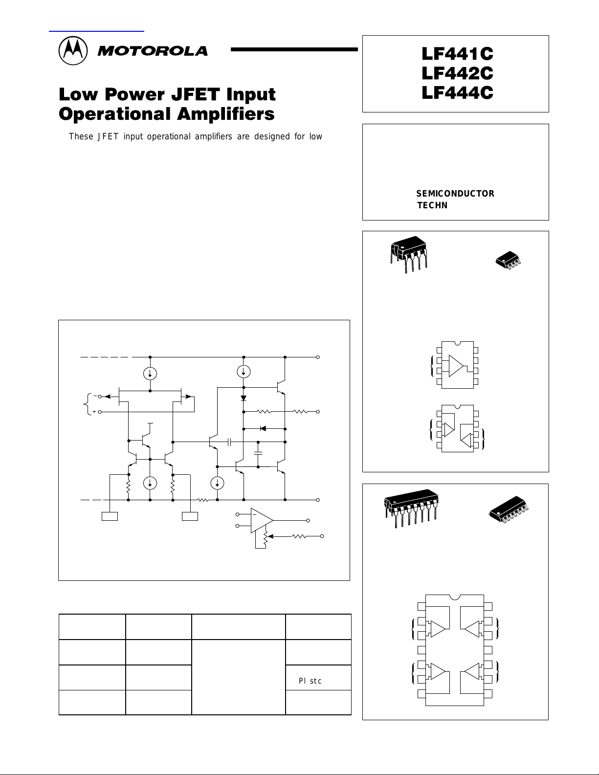
Representative Schematic Diagram
J1 J2
Inputs
Q1 Q2
12
(Each Amplifier)
+
Q3
Ω
Q4
C1
Q5
D2
R3
D1
C2
Q7
Q6
R4
V
CC
Output
LOW POWER
JFET INPUT
OPERATIONAL AMPLIFIERS
SEMICONDUCTOR
TECHNICAL DATA
8
1
N SUFFIX
PLASTIC PACKAGE
CASE 626
PIN CONNECTIONS
Offset Null
Inputs
V
EE
(Single, Top View)
Output 1
Inputs 1
V
EE
(Dual, Top View)
1
2
–
+
3
4
1
1
2
–
+
3
2
4
8
1
D SUFFIX
PLASTIC PACKAGE
CASE 751
(SO–8)
8
NC
7
V
CC
6
Output
5
Offset Null
8
V
CC
7
Output 2
6
–
Inputs 2
+
5
R1 R2
15
*
R5
*
*Null adjustment pins for LF441 only.
ORDERING INFORMATION
Operating
Device Function
LF441CD
Single
Temperature Range
LF441CN
LF442CD
LF442CN
LF444CD
Dual
TA = 0° to +70°C
Quad SO–14
LF444CN
MOTOROLA ANALOG IC DEVICE DATA
+
5
1.5 k
1
100 k
Ω
Ω
LF441C input offset voltage
null adjust circuit
Package
SO–8
Plastic DIP
SO–8
Plastic DIP
Plastic DIP
V
EE
14
V
EE
1
N SUFFIX
PLASTIC PACKAGE
CASE 646
14
1
D SUFFIX
PLASTIC PACKAGE
CASE 751A
(SO–14)
PIN CONNECTIONS
Output 1
Inputs 1
Inputs 2
Output 2
1
––
2
1
3
++
V
4
CC
++
5
23
6
––
78
(Quad, Top View)
Motorola, Inc. 1996 Rev 0
14
Output 4
13
4
Inputs 4
12
11
V
EE
10
Inputs 3
9
Output 3
1
Page 2
LF441C LF442C LF444C
MAXIMUM RATINGS
Rating Symbol Value Unit
Supply Voltage (from VCC to VEE) V
Input Differential V oltage Range (Note 1) V
Input Voltage Range (Notes 1 and 2) V
Output Short Circuit Duration (Note 3) t
Operating Junction Temperature (Note 3) T
Storage Temperature Range T
NOTES: 1. Differential voltages are at the noninverting input terminal with respect to the inverting
input terminal.
2.The magnitude of the input voltage must never exceed the magnitude of the supply
or 15 V, whichever is less.
3.Power dissipation must be considered to ensure maximum junction temperature (TJ)
is not exceeded (see Figure 1).
S
IDR
IR
SC
J
stg
+36 V
±30 V
±15 V
Indefinite sec
+150 °C
–60 to +150 °C
DC ELECTRICAL CHARACTERISTICS (V
Characteristic
Input Offset Voltage (RS = 10 kΩ, VO = 0 V) V
Single: TA = +25°C – 3.0 5.0
TA = 0° to +70°C – – 7.5
Dual: TA = +25°C – 3.0 5.0
TA = 0° to +70°C – – 7.5
Quad: TA = +25°C – 3.0 10
TA = 0° to +70°C – – 12
Average Temperature Coefficient of Offset V oltage ∆VIO/∆T – 10 – µV/°C
(RS = 10 kΩ, VO = 0 V)
Input Offset Current (VCM = 0 V, VO = 0 V) I
TA = +25°C – 0.5 50 pA
TA = 0° to +70°C – – 1.5 nA
Input Bias Current (VCM = 0 V, VO = 0 V) I
TA = +25°C – 3.0 100 pA
TA = 0° to +70°C – – 3.0 nA
Common Mode Input Voltage Range (TA = +25°C) V
Large Signal Voltage Gain (VO = ±10 V, RL = 10 kΩ) A
TA = +25°C 25 60 –
TA = 0° to +70°C 15 – –
Output Voltage Swing (RL = 10 kΩ) VO +
Common Mode Rejection (RS ≤ 10 kΩ, VCM = V
Power Supply Rejection (RS = 100 Ω, VCM = 0 V, VO = 0 V) PSR 70 84 – dB
Power Supply Current (No Load, VO = 0 V) I
Single – 200 250
Dual – 400 500
Quad – 800 1000
= +15 V, VEE = –15 V, TA = 0° to 70°C, unless otherwise noted.)
CC
Symbol Min Typ Max Unit
IO
IO
IB
ICR
VOL
VO –
, VO = 0 V) CMR 70 86 – dB
ICR
D
–
–11
+12
–
+14.5
–12
+14
–14
+11
–
–
–12
mV
V/mV
V
V
µA
2
MOTOROLA ANALOG IC DEVICE DATA
Page 3
LF441C LF442C LF444C
AC ELECTRICAL CHARACTERISTICS (V
Characteristic Symbol Min Typ Max Unit
Slew Rate (Vin = –10 V to +10 V, RL = 10 kΩ, CL = 10 pF, AV = +1.0) SR 0.6 6.0 – V/ µs
Settling Time To within 10 mV t
(AV = –1.0, RL = 10 kΩ, VO = 0 V to +10 V) To within 1.0 mV – 2.2 –
Gain Bandwidth Product (f = 200 kHz) GBW 0.6 2.0 – MHz
Equivalent Input Noise Voltage (RS = 100 Ω, f = 1.0 kHz) e
Equivalent Input Noise Current (f = 1.0 kHz) i
Input Resistance R
Channel Separation (f = 1.0 Hz to 20 kHz) CS – 120 – dB
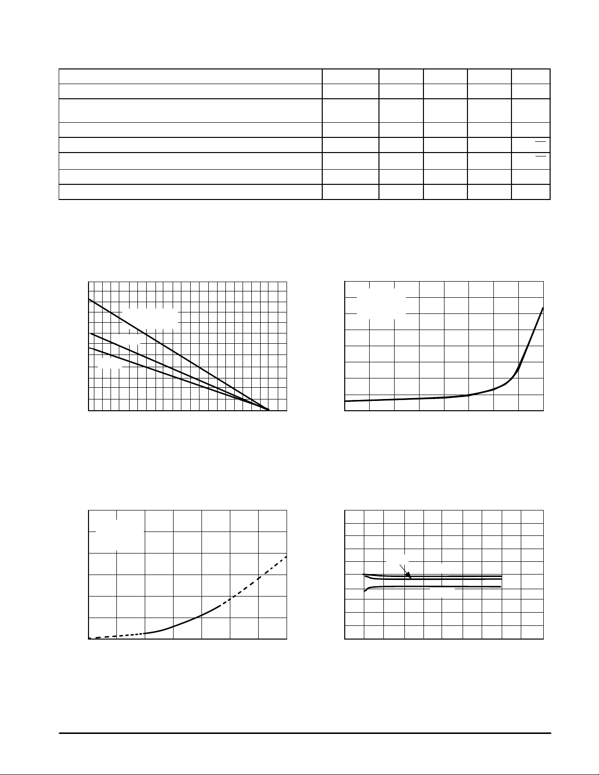
Figure 1. Maximum Power Dissipation versus
T emperature for Package Variations
2400
2000
8 & 14 Pin Plastic
1600
1200
Package
SO–14
= +15 V, VEE = –15 V, TA = +25°C, unless otherwise noted.)
CC
s
n
n
i
– 1.6 – µs
– 47 –
– 0.01 –
– 10
Figure 2. Input Bias Current versus
Input Common Mode Voltage
20
VCC = +15 V
VEE = –15 V
°
C
TA = 25
15
10
12
nV/ Hz√
pA/ Hz√
– Ω
SO–8
800
5.0
, INPUT BIAS CURRENT (pA)
400
MAXIMUM POWER DISSIPATION (mW)
D,
P
0
–55 –40 –20 0 20 40 60 80 100 120 140 160
TA, AMBIENT TEMPERATURE (°C) V
IB
I
0
–10 –5.0 0 5.0 10
, INPUT COMMON MODE VOLTAGE (V)
ICR
Figure 3. Input Bias Current versus T emperature Figure 4. Supply Current versus Supply V oltage
1000
VCC = +15 V
100
VEE = –15 V
VCM = 0 V
10
1.0
0.1
INPUT BIAS CURRENT (nA)
IB,
I
0.01
0.001
–55 –25 0 25 50 75 100 125 0 5.0 10 15 20 25
TA, AMBIENT TEMPERATURE (°C)
300
µ
260
220
180
140
SUPPLY CURRENT PER AMPLIFIER ( A)
D,
I
100
125°C
VCC,
25°C
–55°C
VEE
, SUPPLY VOLTAGE (V)
MOTOROLA ANALOG IC DEVICE DATA
3
Page 4

LF441C LF442C LF444C
Figure 5. Positive Input Common Mode V oltage
Range versus Positive Supply V oltage
20
–55°C ≤ TA ≤ 125°C –55°C ≤ TA ≤ 125°C
15
10
VOLTAGE RANGE (V)
5.0
POSITIVE INPUT COMMON MODE
ICR,
+V
0
VCC, POSITIVE SUPPLY VOLTAGE (V) VEE, NEGATIVE SUPPLY VOLTAGE (V)
Figure 7. Output Voltage versus Output
Source Current
20
15
10
VCC = +15 V
VEE = –15 V
–55°C
25°C
125°C
Figure 6. Negative Input Common Mode V oltage
Range versus Negative Supply V oltage
–20
–15
–10
–5.0
VOLTAGE RANGE (V)
NEGATIVE INPUT COMMON MODE
ICR,
0
2015105.00
–V
0 –5.0 –10 –15 –20
Figure 8. Output Voltage versus
Output Sink Current
–20
VCC = +15 V
VEE = –15 V
–15
–10
125°C
25°C
–55°C
, OUTPUT VOLTAGE (V)
5.0
O
V
0
1.0 2.0 3.0 4.0 5.0 6.0 7.0 8.0 2.0 4.0 6.0 8.0 10 12 14 16 18 20
0
IO, OUTPUT SOURCE CURRENT (mA) –IO, OUTPUT SINK CURRENT (mA)
Figure 9. Output Voltage Swing
versus Supply V oltage
40
)
35
p–p
30
25
20
15
10
, OUTPUT VOL TAGE SWING (V
5.0
O
V
RL = 10 k
Ω
–55°C ≤ TA ≤ 125°C
0
0 2.0 4.0 6.0 8.0 10 12 14 16 1.0 k 2.0 k 3.0 k 4.0 k 6.0 k 8.0 k 10 k
VCC,
VEE
, SUPPLY VOLTAGE (V) RL, LOAD RESISTANCE (Ω)
–5.0
, OUTPUT VOLTAGE (V)
O
V
0
0
)
28
p–p
26
24
22
20
18
, OUTPUT VOL TAGE SWING (V
O
16
V
Figure 10. Output Voltage Swing
versus Load Resistance
VCC = +15 V
VEE = –15 V
°
TA = 25
C
4
MOTOROLA ANALOG IC DEVICE DATA
Page 5

LF441C LF442C LF444C
Figure 11. Normalized Gain Bandwidth
Product versus T emperature
1.4
1.3
1.2
1.1
1.0
0.9
0.8
0.7
0.6
GBW, NORMALIZED GAIN BANDWIDTH PRODUCT
–75 –50 –25 0 25 50 75 100 125
TA, AMBIENT TEMPERATURE (°C) f, FREQUENCY (MHz)
VCC = +15 V
VEE = –15 V
RL = 10 k
CL = 100 pF
Figure 13. Slew Rate versus T emperature
8.0
s)
µ
7.0
Figure 12. Open Loop V oltage Gain and
Phase versus Frequency
Ω
20
10
0
VCC = +15 V
VEE = –15 V
–10
, OPEN LOOP VOL TAGE GAIN (dB)
VOL
–20
A
0.1 1.0 10
Ω
RL = 10 k
CL = 100 pF
°
C
TA = 25
Phase
Gain
90
135
180
225
EXCESS PHASE (DEGREES)
φ,
270
Figure 14. Total Output Distortion
versus Frequency
2.5
VCC = +15 V
VEE = –15 V
2.0
TA = 25
°
C
6.0
SR, SLEW RATE (V/
VCC = +15 V
5.0
VEE = –15 V
Ω
RL = 10 k
AV = +1.0
4.0
–75 –50 –25 0 25 50 75 100 125
TA, AMBIENT TEMPERATURE (°C) f, FREQUENCY (Hz)
Figure 15. Output Voltage Swing
versus Frequency
)
p–p
30
20
VCC = +15 V
VEE = –15 V
10
, OUTPUT VOL TAGE SWING (V
O
V
0
1.0 k
RL = 10 k
AV = +1.0
1% THD
°
TA = 25
Ω
C
10 k
f, FREQUENCY (Hz) f, FREQUENCY (Hz)
100 k 1.0 M
1.5
1.0
AV = 100
0.5
THD, OUTPUT DISTORTION (%)
0
10 100 1.0 k 10 k 100 k
AV = 10
Figure 16. Open Loop V oltage
Gain versus Frequency
100
80
60
40
VCC = +15 V
, OPEN LOOP VOL TAGE GAIN (dB)
VEE = –15 V
20
VOL
A
0
0.1 1.0 10 100 1.0 k 10 k 100 k 1.0 M 10 M
RL = 10 k
TA = 25°C
Ω
MOTOROLA ANALOG IC DEVICE DATA
5
Page 6

LF441C LF442C LF444C
Figure 17. Common Mode Rejection
versus Frequency
140
120
100
80
60
VCC = +15 V
40
VEE = –15 V
VCM = 0 V
20
∆
VCM = ±1.5 V
°
C
TA = 25
0
CMR, COMMON MODE REJECTION (dB)
100 1.0 k 10 k 100 k 1.0 M
∆
V
CM
CMR = 20 Log
f, FREQUENCY (Hz) f, FREQUENCY (Hz)
A
DM
+
∆
V
CM
x A
()
DM
∆
V
O
Figure 19. Input Noise V oltage versus Frequency
70
)
Hz
√
60
nV/
50
Figure 18. Power Supply Rejection
versus Frequency
140
VCC = +15 V
VEE = –15 V
∆
V
O
120
100
80
60
40
20
0
PSR, POWER SUPPLY REJECTION (dB)
100 1.0 k 10 k 100 k 1.0 M
°
C
TA = 25
+PSR = 20 Log
–PSR = 20 Log
–PSR
∆
VO /A
(
∆
∆
VO /A
(
∆
+PSR
(∆VEE=±1.5 V)
DM
)
V
CC
DM
)
V
EE
∆
V
CC
–
A
DM
+
(∆VCC = ±1.5 V)
∆
V
∆
V
EE
O
Figure 20. Open Loop V oltage
Gain versus Supply V oltage
1.0 M
RL = 10 k
Ω
40
30
20
INPUT NOISE VOLTAGE (
10
n
e ,
0
10 100 1.0 k 10 k 100 k
f, FREQUENCY (Hz)
VCC = +15 V
VEE = –15 V
VCM = 0 V
TA = 25
°
C
100 k
25°C
, OPEN LOOP VOL TAGE GAIN (V V)
VOL
A
10 k
0 5.0 10 15 20 25
VCC, VEE, SUPPLY VOLTAGE (V)
Figure 21. Output Impedance versus Frequency Figure 22. Inverter Settling Time
350
VCC = +15 V
300
)
Ω
, OUTPUT IMPEDANCE (
O
Z
VEE = –15 V
°
C
TA = 25
250
200
150
100
50
0
100 1.0k 10k 100k 1.0M
AV = 100 AV = 10 AV = 1.0
f, FREQUENCY (Hz)
–5.0
, OUTPUT VOL TAGE STEP FROM 0 V (V)
O
V
VCC = +15 V
10
VEE = –15 V
°
C
TA = 25
5.0
0
–10
0.1 1.0 10
10 mV
10 mV
ts, SETTLING TIME (
1.0 mV
1.0 mV
µ
s)
125°C
–55°C
6
MOTOROLA ANALOG IC DEVICE DATA
Page 7

LF441C LF442C LF444C
SMALL SIGNAL RESPONSE
Figure 23. Inverting Figure 24. Noninverting
VCC = +15 V
VEE = –15 V
Ω
RL = 10 k
CL = 10 pF
AV = –1.0
°
C
TA = 25
0
, OUTPUT VOLTAGE (50 mV/DIV)
O
V
VCC = +15 V
VEE = –15 V
Ω
RL = 10 k
CL = 10 pF
AV = +1.0
°
C
TA = 25
0
, OUTPUT VOLTAGE (50 mV/DIV)
O
V
t, TIME (0.5
µ
s/DIV)
t, TIME (0.5 µs/DIV)
LARGE SIGNAL RESPONSE
Figure 25. Inverting Figure 26. Noninverting
VCC = +15 V
VEE = –15 V
RL = 10 k
CL = 10 pF
AV = –1.0
°
TA = 25
0
, OUTPUT VOLTAGE (5.0 V/DIV)
O
V
VCC = +15 V
Ω
C
µ
t, TIME (2.0
s/DIV)
VEE = –15 V
RL = 10 k
CL = 10 pF
AV = +1.0
°
TA = 25
0
, OUTPUT VOLTAGE (5.0 V/DIV)
O
V
Ω
C
µ
t, TIME (2.0
s/DIV)
MOTOROLA ANALOG IC DEVICE DATA
7
Page 8

NOTE 2
–T–
SEATING
PLANE
H
LF441C LF442C LF444C
OUTLINE DIMENSIONS
58
–B–
14
F
–A–
C
N
D
G
0.13 (0.005) B
K
M
T
N SUFFIX
PLASTIC PACKAGE
CASE 626–05
ISSUE K
L
J
M
M
A
M
NOTES:
1. DIMENSION L TO CENTER OF LEAD WHEN
FORMED PARALLEL.
2. PACKAGE CONTOUR OPTIONAL (ROUND OR
SQUARE CORNERS).
3. DIMENSIONING AND TOLERANCING PER ANSI
Y14.5M, 1982.
DIM MIN MAX MIN MAX
A 9.40 10.16 0.370 0.400
B 6.10 6.60 0.240 0.260
C 3.94 4.45 0.155 0.175
D 0.38 0.51 0.015 0.020
F 1.02 1.78 0.040 0.070
G 2.54 BSC 0.100 BSC
H 0.76 1.27 0.030 0.050
J 0.20 0.30 0.008 0.012
K 2.92 3.43 0.115 0.135
L 7.62 BSC 0.300 BSC
M ––– 10 ––– 10
N 0.76 1.01 0.030 0.040
INCHESMILLIMETERS
__
A
C
A1
D SUFFIX
PLASTIC PACKAGE
CASE 751–05
(SO–8)
ISSUE R
D
58
0.25MB
E
1
B
e
H
4
M
h
X 45
_
q
C
A
SEATING
PLANE
0.10
L
B
SS
A0.25MCB
NOTES:
1. DIMENSIONING AND TOLERANCING PER ASME
Y14.5M, 1994.
2. DIMENSIONS ARE IN MILLIMETERS.
3. DIMENSION D AND E DO NOT INCLUDE MOLD
PROTRUSION.
4. MAXIMUM MOLD PROTRUSION 0.15 PER SIDE.
5. DIMENSION B DOES NOT INCLUDE MOLD
PROTRUSION. ALLOWABLE DAMBAR
PROTRUSION SHALL BE 0.127 TOTAL IN EXCESS
OF THE B DIMENSION AT MAXIMUM MATERIAL
CONDITION.
MILLIMETERS
DIM MIN MAX
A 1.35 1.75
A1 0.10 0.25
B 0.35 0.49
C 0.18 0.25
D 4.80 5.00
E
3.80 4.00
1.27 BSCe
H 5.80 6.20
h
0.25 0.50
L 0.40 1.25
0 7
q
__
8
MOTOROLA ANALOG IC DEVICE DATA
Page 9

LF441C LF442C LF444C
OUTLINE DIMENSIONS
N SUFFIX
PLASTIC PACKAGE
CASE 646–06
ISSUE L
14 8
B
17
A
F
N
SEATING
HG D
PLANE
C
K
L
J
M
NOTES:
1. LEADS WITHIN 0.13 (0.005) RADIUS OF TRUE
POSITION AT SEATING PLANE AT MAXIMUM
MATERIAL CONDITION.
2. DIMENSION L TO CENTER OF LEADS WHEN
FORMED PARALLEL.
3. DIMENSION B DOES NOT INCLUDE MOLD
FLASH.
4. ROUNDED CORNERS OPTIONAL.
DIM MIN MAX MIN MAX
A 0.715 0.770 18.16 19.56
B 0.240 0.260 6.10 6.60
C 0.145 0.185 3.69 4.69
D 0.015 0.021 0.38 0.53
F 0.040 0.070 1.02 1.78
G 0.100 BSC 2.54 BSC
H 0.052 0.095 1.32 2.41
J 0.008 0.015 0.20 0.38
K 0.115 0.135 2.92 3.43
L 0.300 BSC 7.62 BSC
M 0 10 0 10
____
N 0.015 0.039 0.39 1.01
MILLIMETERSINCHES
–T–
SEATING
PLANE
–A–
14 8
G
D 14 PL
0.25 (0.010) A
D SUFFIX
PLASTIC PACKAGE
CASE 751A–03
(SO–14)
ISSUE F
NOTES:
1. DIMENSIONING AND TOLERANCING PER ANSI
Y14.5M, 1982.
2. CONTROLLING DIMENSION: MILLIMETER.
3. DIMENSIONS A AND B DO NOT INCLUDE
MOLD PROTRUSION.
4. MAXIMUM MOLD PROTRUSION 0.15 (0.006)
–B–
71
M
7 PL
P
M
0.25 (0.010) B
X 45
C
R
K
S
B
T
S
M
_
M
F
J
PER SIDE.
5. DIMENSION D DOES NOT INCLUDE DAMBAR
PROTRUSION. ALLOWABLE DAMBAR
PROTRUSION SHALL BE 0.127 (0.005) TOTAL
IN EXCESS OF THE D DIMENSION AT
MAXIMUM MATERIAL CONDITION.
DIM MIN MAX MIN MAX
A 8.55 8.75 0.337 0.344
B 3.80 4.00 0.150 0.157
C 1.35 1.75 0.054 0.068
D 0.35 0.49 0.014 0.019
F 0.40 1.25 0.016 0.049
G 1.27 BSC 0.050 BSC
J 0.19 0.25 0.008 0.009
K 0.10 0.25 0.004 0.009
M 0 7 0 7
____
P 5.80 6.20 0.228 0.244
R 0.25 0.50 0.010 0.019
INCHESMILLIMETERS
MOTOROLA ANALOG IC DEVICE DATA
9
Page 10

LF441C LF442C LF444C
Motorola reserves the right to make changes without further notice to any products herein. Motorola makes no warranty , representation or guarantee regarding
the suitability of its products for any particular purpose, nor does Motorola assume any liability arising out of the application or use of any product or circuit, and
specifically disclaims any and all liability, including without limitation consequential or incidental damages. “T ypical” parameters which may be provided in Motorola
data sheets and/or specifications can and do vary in different applications and actual performance may vary over time. All operating parameters, including “Typicals”
must be validated for each customer application by customer’s technical experts. Motorola does not convey any license under its patent rights nor the rights of
others. Motorola products are not designed, intended, or authorized for use as components in systems intended for surgical implant into the body, or other
applications intended to support or sustain life, or for any other application in which the failure of the Motorola product could create a situation where personal injury
or death may occur. Should Buyer purchase or use Motorola products for any such unintended or unauthorized application, Buyer shall indemnify and hold Motorola
and its officers, employees, subsidiaries, affiliates, and distributors harmless against all claims, costs, damages, and expenses, and reasonable attorney fees
arising out of, directly or indirectly, any claim of personal injury or death associated with such unintended or unauthorized use, even if such claim alleges that
Motorola was negligent regarding the design or manufacture of the part. Motorola and are registered trademarks of Motorola, Inc. Motorola, Inc. is an Equal
Opportunity/Affirmative Action Employer.
How to reach us:
USA/EUROPE/Locations Not Listed: Motorola Literature Distribution; JAPAN: Nippon Motorola Ltd.; Tatsumi–SPD–JLDC, 6F Seibu–Butsuryu–Center,
P.O. Box 20912; Phoenix, Arizona 85036. 1–800–441–2447 or 602–303–5454 3–14–2 T atsumi Koto–Ku, Tokyo 135, Japan. 03–81–3521–8315
MFAX: RMF AX0@email.sps.mot.com – TOUCHT ONE 602–244–6609 ASIA/PACIFIC: Motorola Semiconductors H.K. Ltd.; 8B T ai Ping Industrial Park,
INTERNET: http://Design–NET.com 51 Ting Kok Road, Tai Po, N.T., Hong Kong. 852–26629298
10
◊
MOTOROLA ANALOG IC DEVICE DATA
LF441C/D
*LF441C/D*
 Loading...