

Page 1
DEVICES INCORPORATED
LF43891
9 x 9-bit Digital Filter
LF43891
DEVICES INCORPORATED
FEATURES DESCRIPTION
❑❑
❑ 30 MHz Maximum Sampling Rate
❑❑
❑❑
❑ 320 MHz Multiply-Accumulate Rate
❑❑
❑❑
❑ 8 Filter Cells
❑❑
❑❑
❑ 8-bit Unsigned or 9-bit Two’s
❑❑
Complement Data/Coefficients
❑❑
❑ 26-bit Data Outputs
❑❑
❑❑
❑ Shift-and-Add Output Stage for
❑❑
Combining Filter Outputs
❑❑
❑ Expandable Data Size, Coefficient
❑❑
Size, and Filter Length
❑❑
❑ User-Selectable 2:1, 3:1, or 4:1
❑❑
Decimation
❑❑
❑ Replaces Harris HSP43891
❑❑
❑❑
❑ 84-pin PLCC, J-Lead
❑❑
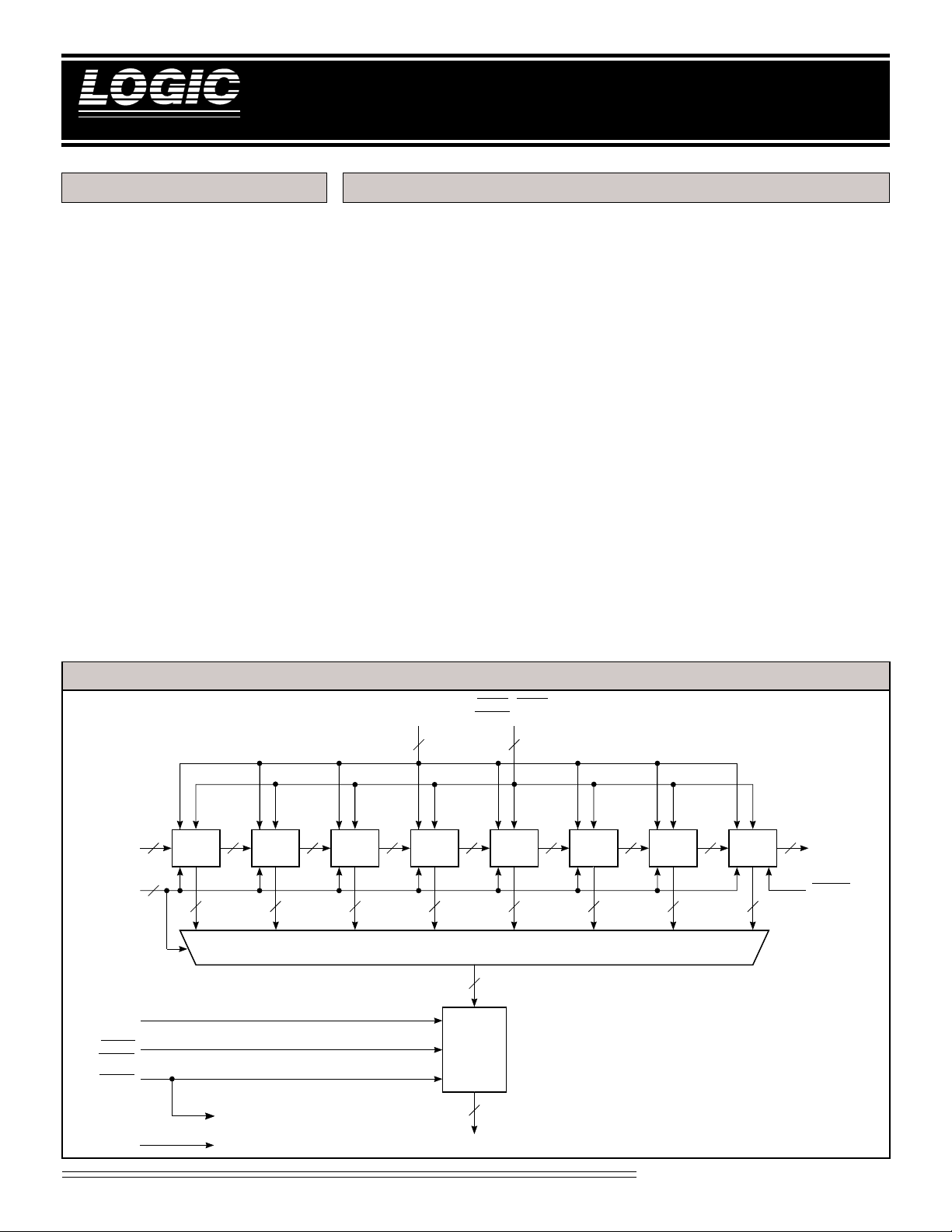
The LF43891 is a video-speed digital
filter that contains eight filter cells
(taps) cascaded internally and a shiftand-add output stage. A 9 x 9 multiplier, three decimation registers, and a
26-bit accumulator are contained in
each filter cell. The output stage of the
LF43891 contains a 26-bit accumulator
which can add the contents of any
filter stage to the output stage accumulator shifted right by 8 bits. 8-bit
unsigned or 9-bit two’s complement
format for data and coefficients can be
independently selected.
Expanded coefficients and word sizes
can be processed by cascading multiple LF43891s to implement larger
filter lengths without affecting the
sample rate. By reducing the sample
9 x 9-bit Digital Filter
rate, a single LF43891 can process
larger filter lengths by using multiple
passes. The sampling rate can range
from 0 to 40 MHz. Over 1000 taps
may be processed without overflows
due to the architecture of the device.
The output sample rate can be reduced to one-half, one-third, or onefourth the input sample rate by using
the three decimation registers contained in every filter cell. Matrix
multiplication, N x N spatial correlations/convolutions, and other 2-D
operations for image processing can
also be achieved using these registers.
LF43891 BLOCK DIAGRAM
CIN
8-0
ADR
2-0
SHADD
SENBL
SENBH
RESET
9
3
FILTER
CELL 0
9
FILTER
CELL 1
TO ALL CELLS
DIN
8-0
9
9 9
FILTER
CELL 2
2626 26 26 26 26 26 26
FILTER
CELL 3
DIENB, CIENB,
ERASE, DCM
9
MUX
26
OUTPUT
STAGE
26
5
FILTER
CELL 4
1-0
9
FILTER
CELL 5
9
FILTER
CELL 6
9
FILTER
CELL 7
9
COUT
COENB
8-0
SUM
TO ALL REGISTERSCLK
25-0
Video Imaging Products
1
08/16/2000–LDS.43891-J
Page 2
DEVICES INCORPORATED
)
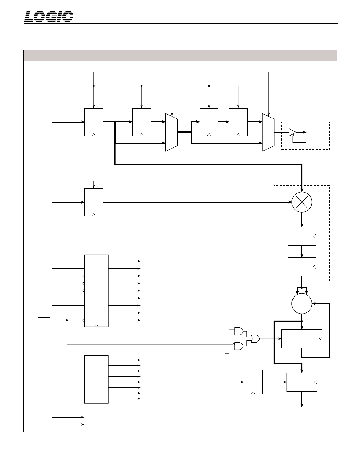
FIGURE 1. FILTER CELL DIAGRAM
LF43891
9 x 9-bit Digital Filter
DCM0.D DCM1.DCIENB.D
CIN8-0
DIENB.D
DIN8-0
DCM1
DCM0
RESET
DIENB
CIENB
ADR
ADR1
ADR2
ERASE
LD
C
C REG
LD
X REG
LATCHES
0
8-0
LD
D1 REG
DCM1.D
DCM
RESET.D
DIENB.D
CIENB.D
ADR
ADR
ADR
ERASE.D
0.D
0.D
1.D
2.D
LD
1
MUX
0
D2 REG
RESET.D
ERASE.D
D8-0
C8-0
X8-0
LD
D3 REG
1
MUX
0
SIGN EXTENSION
TRI-STATE BUFFER
ON FILTER CELL 7 ONLY
COUT8-0
COENB
M REG0
M REG1
25-18
ACC25-0
ACCUMULATOR
17-0
CELL 0
CELL 1
ADR0
ADR1
ADR2
CLK TO ALL REGISTERS
RESET.D TO ALL REGISTERS (EXCEPT ACCUMULATOR AND T-REGISTER
DECODER
CELL 2
CELL 3
CELL 4
CELL 5
CELL 6
CELL 7
2
CELL n
CELL n
ACC.D25-0
DQ
LD
T REG
AOUT
25-0
Video Imaging Products
08/16/2000–LDS.43891-J
Page 3
DEVICES INCORPORATED
LF43891
9 x 9-bit Digital Filter
FILTER CELL DESCRIPTION
9-bit coefficients are loaded into the
C register (CIN8-0) and are output as
COUT8-0 (the COENB signal enables
the COUT8-0 outputs). The path
taken by the coefficients varies
according to the decimation mode
chosen. With no decimation, the
coefficients move directly from the
C register, bypassing all decimation
registers, and are available at the
output on the following clock cycle.
When decimation is chosen, the
coefficient output is delayed by 1, 2,
or 3 clock cycles depending on how
many decimation registers the
coefficients pass through (D1, D2, or
D3). The number of decimation
registers the coefficients pass
through is determined by DCM1-0.
Refer to Table 1 for choosing a
decimation mode.
CIENB enables the C and D registers
for coefficient loading. The registers
are loaded on the rising edge of CLK
when CIENB is LOW. CIENB is
latched and delayed internally which
enables the registers for loading one
clock cycle after CIENB goes active
(loading takes place on the second
rising edge of CLK after CIENB goes
LOW). Therefore, CIENB must be
LOW one clock cycle before the
coefficients are placed on the CIN8-0
inputs. The coefficients are held when
CIENB is HIGH.
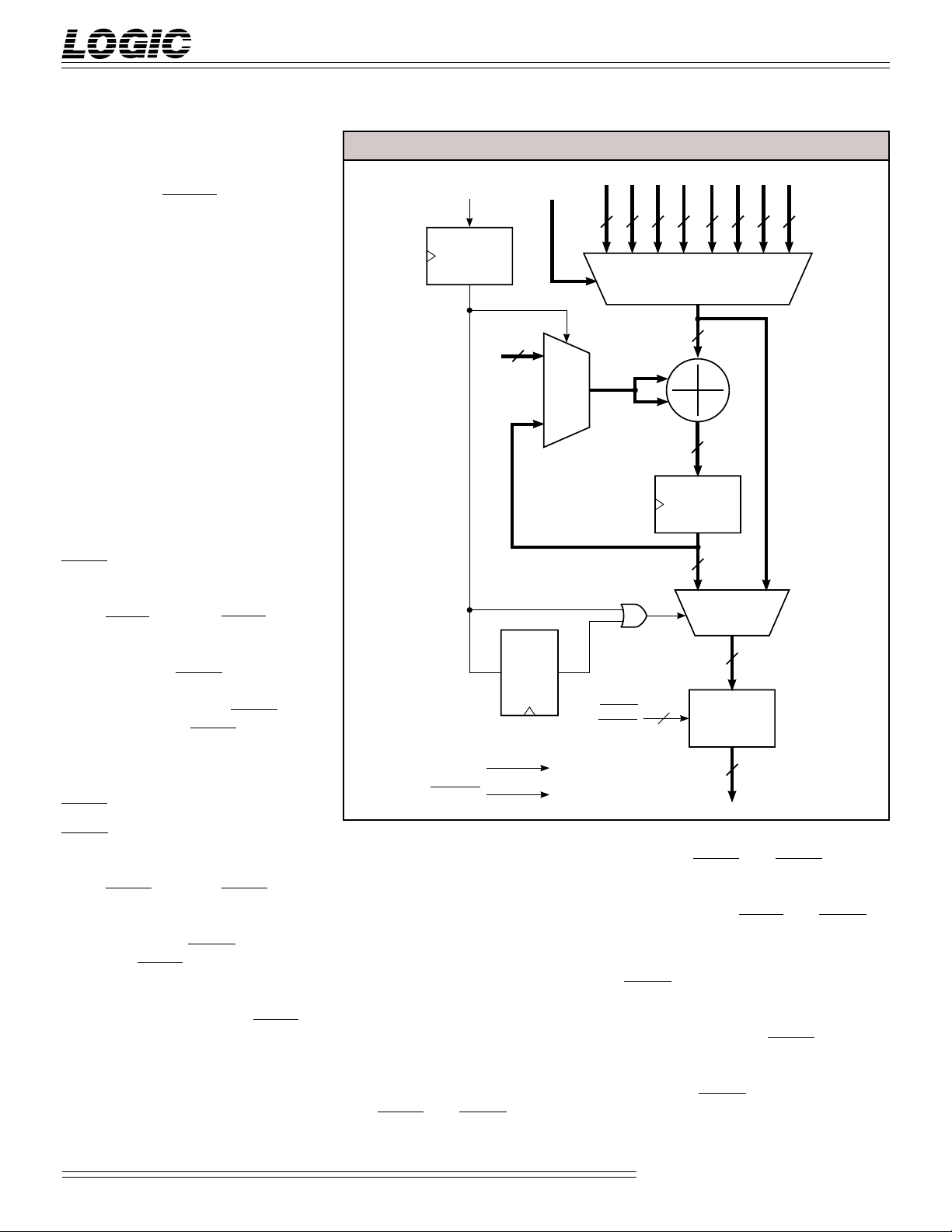
FIGURE 2. OUTPUT STAGE DIAGRAM
SHADD
D
Q
CLK
RESET.D
ADR
18
0
DQ
2-0
.D
26 26 26
01
EXTENSION
17-0
MUX
ZERO
25-8
SENBL
SENBH
TO ALL REGISTERS
TO ALL REGISTERS
CELL RESULT
SIGN
25-18
17-0
OUTPUT
BUFFER
2
MUX
26
26
26
OUTPUT
TRI-STATE
BUFFER
2626262626
01
MUX
26
26
DIENB enables the X register for the
loading of data. The X register is
loaded on the rising edge of CLK
when DIENB is LOW. DIENB is
latched and delayed internally (loading takes place on the second rising
edge of CLK after DIENB goes LOW).
Therefore, DIENB must be LOW one
clock cycle before the data is placed on
the DIN8-0 inputs. The X register is
loaded with all zeros when DIENB is
HIGH.
The output of the C register (C8-0) and
X register (X8-0) provide the inputs of
the 9 x 9 multiplier. The multiplier is
followed by two pipeline registers,
M REG0 and M REG1. The output of
the multiplier is sign extended and is
used as one of the inputs to the 26-bit
adder. The output of the 26-bit
accumulator provides the second
input to the adder. Both the accumulator and T register are loaded simultaneously with the output of the
adder.
The accumulator is loaded with the
output of the adder on every clock
cycle unless cleared. Clearing the
accumulator can be achieved using
two methods. The first method, when
both RESET and ERASE are LOW,
causes all accumulators and all
3
registers in the device to be cleared
together. RESET and ERASE are
latched and delayed internally causing the clearing to occur on the second
clock cycle after RESET and ERASE go
active.
The second method, when only
ERASE is LOW, clears a single accumulator of a selected cell. The cell is
selected using the ADR2-0 inputs
(decoded to Cell n). ERASE is latched
and delayed internally causing the
clearing to occur on the second clock
cycle after ERASE goes active. Refer
to Table 2 for clearing registers and
accumulators.
Video Imaging Products
08/16/2000–LDS.43891-J
Page 4
DEVICES INCORPORATED
LF43891
9 x 9-bit Digital Filter
TABLE 1. DECIMATION MODE SELECTION
DCM1 DCM0 Decimation Function
0 0 Decimation registers not used
0 1 One decimation register used (decimation by one-half)
1 0 Two decimation registers used (decimation by one-third)
1 1 Three decimation registers used (decimation by one-fourth)
TABLE 2. REGISTER AND ACCUMULATOR CLEARING
ERASE RESET Clearing Effect
0 0 All accumulators and all registers are cleared
0 1 Only the accumulator addressed by ADR2-0 is cleared
1 0 All registers are cleared (accumulators are not cleared)
1 1 No clearing occurs, internal state remains the same
OUTPUT STAGE DESCRIPTION
The 26-bit adder contained in the
output stage can add the contents of
any filter cell accumulator (selected by
ADR2-0) with the 18 most significant
bits of the output buffer. The result is
stored back into the output buffer.
The complete operation takes only one
clock cycle. The eight least significant
bits of the output buffer are lost.
The Zero multiplexer is controlled by
the SHADD input signal. This allows
selection of either the 18 most significant bits of the output buffer or all
zeros for the adder input. When
SHADD is LOW, all zeros will be
selected. When SHADD is HIGH, the
18 most significant bits of the output
buffer are selected enabling the shiftand-add operation. SHADD is
latched and delayed internally by one
clock cycle.
The output multiplexer is also controlled by the SHADD input signal.
This allows selection of either a filter
cell accumulator, selected by ADR2-0,
or the output buffer to be output to
the SUM25-0 bus. Only the 26 least
significant bits from either a filter cell
accumulator or the output buffer are
output on SUM25-0. If SHADD is
LOW during two consecutive clock
cycles (low during the current and
previous clock cycle), the output
multiplexer selects the contents of a
filter cell accumulator addressed by
ADR2-0. Otherwise, the output
multiplexer selects the contents of the
output buffer.
If the same address remains on the
ADR2-0 inputs for more than one clock
cycle, SUM25-0 will not change to
reflect any updates to the addressed
cell accumulator. Only the result from
the first selection of the cell (first clock
cycle) will be output. This allows the
interface of slow memory devices
where the output needs to be active
for more than one clock cycle. Normal
FIR operation is not affected because
ADR2-0 is changed sequentially.
NUMBER SYSTEMS
Data and coefficients can be represented as either 8-bit unsigned or 9-bit
two's complement numbers. All
values are represented as 9-bit two's
complement numbers internally. If
the most significant or sign bit is a
zero, the multiplier can multiply 8-bit
unsigned numbers.
SIGNAL DEFINITIONS
Power
VCC and GND
+5 V power supply. All pins must be
connected.
Clock
CLK — Master Clock
The rising edge of CLK strobes all
registers. All timing specifications are
referenced to the rising edge of CLK.
Inputs
DIN8-0 — Data Input
9-bit data is latched into the X register
of each filter cell simultaneously. The
DIENB signal enables loading of the
data.
CIN8-0 — Coefficient Input
9-bit coefficients are latched into the C
register of Filter Cell 0. The CIENB
signal enables loading of the coefficients.
Outputs
SUM25-0 — Data Output
The 26-bit result from an individual
filter cell will appear when ADR2-0 is
used to select the filter cell result.
SHADD in conjunction with ADR2-0 is
used to select the output from the
shift-and-add output stage.
COUT8-0 — Coefficient Output
The 9-bit coefficient output from
Filter Cell 7 can be connected to the
CIN8-0 coefficient input of the same
LF43891 to recirculate the coefficients.
COUT8-0 can also be connected to the
CIN8-0 of another LF43891 to cascade
the devices. The COENB signal
enables the output of the coefficients.
Video Imaging Products
4
08/16/2000–LDS.43891-J
Page 5

DEVICES INCORPORATED
LF43891
9 x 9-bit Digital Filter
Controls
DIENB — Data Input Enable
The DIENB input enables the X
register of every filter cell. While
DIENB is LOW, the X registers are
loaded with the data present at the
DIN8-0 inputs on the rising edge of
CLK. While DIENB is HIGH, all bits
of DIN8-0 are forced to zero and a
rising edge of CLK will load the X
register of every filter cell with all
zeros. DIENB must be low one clock
cycle prior to presenting the input
data on the DIN8-0 input since it is
latched and delayed internally.
CIENB — Coefficient Input Enable
The CIENB input enables the C and D
registers of every filter cell. While
CIENB is LOW, the C and appropriate
D registers are loaded with the
coefficient data on the rising edge of
CLK. While CIENB is HIGH, the
contents of the C and D registers are
held and the CLK signal is ignored.
By using CIENB in its active state,
coefficient data can be shifted from
cell to cell. CIENB must be low one
clock cycle prior to presenting the
coefficient data on the CIN8-0 input
since it is latched and delayed internally.
COENB — Coefficient Output Enable
The COENB input enables the
COUT8-0 output. When COENB is
LOW, the outputs are enabled. When
COENB is HIGH, the outputs are
placed in a high-impedance state.
DCM1-0 — Decimation Control
The DCM1-0 inputs select the number of decimation registers to use
(Table 1). Coefficients are passed
from one cell to another at a rate
determined by DCM1-0. When no
decimation registers are selected,
the coefficients are passed from cell
to cell on every rising edge of CLK
(no decimation). When one decimation register is selected, the coefficients are passed from cell to cell on
every other rising edge of CLK (2:1
decimation). When two decimation
registers are selected, the coefficients are passed from cell to cell on
every third rising edge of CLK (3:1
decimation) and so on. DCM1-0 is
latched and delayed internally.
ADR2-0 — Cell Accumulator Select
The ADR2-0 inputs select which cell’s
accumulator will available at the
SUM25-0 output or added to the
output stage accumulator. In both
cases, ADR2-0 is latched and delayed
by one clock cycle. If the same
address remains on the ADR2-0 inputs
for more than one clock cycle,
SUM25-0 will not change if the contents of the accumulator changes.
Only the result from the first selection
of the cell (first clock cycle) by ADR2-0
will be available. ADR2-0 is also used
to select which accumulator to clear
when ERASE is LOW.
SENBH — MSB Output Enable
When SENBH is LOW, SUM25-16 is
enabled. When SENBH is HIGH,
SUM25-16 is placed in a high-impedance state.
SENBL — LSB Output Enable
When SENBL is LOW, SUM15-0 is
enabled. When SENBL is HIGH,
SUM15-0 is placed in a high-impedance state.
RESET — Register Reset Control
When RESET is LOW, all registers are
cleared simultaneously except the cell
accumulators. RESET can be used
with ERASE to clear all cell accumulators. RESET is latched and delayed
internally. Refer to Table 2.
ERASE — Accumulator Erase Control
When ERASE is LOW, the cell accumulator specified by ADR2-0 is
cleared. When RESET is LOW in
conjunction with ERASE, all cell
accumulators are cleared. Refer to
Table 2.
Video Imaging Products
5
08/16/2000–LDS.43891-J
Page 6

DEVICES INCORPORATED
LF43891
9 x 9-bit Digital Filter
MAXIMUM RATINGS
Storage temperature ........................................................................................................... –65°C to +150°C
Operating ambient temperature........................................................................................... –55°C to +125°C
VCC supply voltage with respect to ground............................................................................ –0.5 V to +7.0V
Input signal with respect to ground ............................................................................... –0.5 V to VCC + 0.5 V
Signal applied to high impedance output ...................................................................... –0.5 V to VCC + 0.5 V
Output current into low outputs............................................................................................................. 25 mA
Latchup current ............................................................................................................................... > 400 mA
OPERATING CONDITIONS
Active Operation, Commercial 0°C to +70°C 4.75 V ≤ VCC ≤ 5.25 V
Active Operation, Military –55°C to +125°C 4.50 V ≤ VCC ≤ 5.50 V
ELECTRICAL CHARACTERISTICS
Above which useful life may be impaired (Notes 1, 2, 3, 8)
To meet specified electrical and switching characteristics
Mode Temperature Range (Ambient) Supply Voltage
Over Operating Conditions (Note 4)
Symbol Parameter Test Condition Min Typ Max Unit
VOH Output High Voltage VCC = Min., IOH = –400 µA 2.6 V
VOL Output Low Voltage VCC = Min., IOL = 2.0 mA 0.4 V
VIH Input High Voltage 2.0 VCC V
V IL Input Low Voltage (Note 3) 0.0 0.8 V
IIX Input Current Ground ≤ VIN ≤ VCC (Note 12) ±10 µA
IOZ Output Leakage Current (Note 12) ±10 µA
ICC1 VCC Current, Dynamic (Notes 5, 6) 160 mA
ICC2 VCC Current, Quiescent (Note 7) 750 µA
CIN Input Capacitance TA = 25°C, f = 1 MHz 10 pF
COUT Output Capacitance TA = 25°C, f = 1 MHz 10 pF
Video Imaging Products
6
08/16/2000–LDS.43891-J
Page 7

DEVICES INCORPORATED
3
3
3
3
3
3
3
3
3
3
3
3
3
3
3
3
3
3
3
3
3
3
3
3
3
3
3
3
3
3
3
3
3
3
3
3
3
3
3
3
3
3
3
3
3
3
3
3
3
3
3
3
3
3
3
3
3
3
5
5
5
5
5
5
5
5
5
5
5
5
5
5
5
5
5
5
5
5
5
5
5
5
5
5
5
5
5
4
SWITCHING CHARACTERISTICS
LF43891
9 x 9-bit Digital Filter
COMMERCIAL OPERATING RANGE (0°C to +70°C)
Symbol Parameter Min Max Min Max Min Max Min Max
tCYC Cycle Time 50 39 3 3 25
tPW Clock Pulse Width 20 16 13 10
tS Input Setup Time 16 14 13 10
tH Input Hold Time 0000
tODC Coefficient Output Delay 24 20 18 16
tODS Sum Output Delay 27 25 21 18
tENA Three-State Output Enable Delay (Note 11) 20 15 15 12
tDIS Three-State Output Disable Delay (Note 11) 20 15 15 12
MILITARY OPERATING RANGE (–55°C to +125°C)
Notes 9, 10 (ns)
23456789012
23456789012
50
23456789012
23456789012
23456789012
23456789012
23456789012
23456789012
23456789012
23456789012
23456789012
23456789012
23456789012
23456789012
23456789012
23456789012
23456789012
23456789012
23456789012
23456789012
23456789012
23456789012
23456789012
23456789012
23456789012
23456789012
23456789012
23456789012
23456789012
Notes 9, 10 (ns)
LF43891–
*
40 33 25
23456789012
23456789012
23456789012
23456789012
23456789012
23456789012
23456789012
23456789012
23456789012
23456789012
23456789012
23456789012
23456789012
23456789012
23456789012
23456789012
23456789012
23456789012
23456789012
23456789012
23456789012
23456789012
23456789012
23456789012
23456789012
23456789012
23456789012
23456789012
23456789012
*
LF43891–
23456789012345678901234567890121234
23456789012345678901234567890121234
23456789012345678901234567890121234
Symbol Parameter Min Max Min Max Min Max
tCYC Cycle Time 50 39 33
tPW Clock Pulse Width 20 16 13
tS Input Setup Time 20 17 13
tH Input Hold Time 0 0 0
tODC Coefficient Output Delay 24 20 18
tODS Sum Output Delay 31 25 21
tENA Three-State Output Enable Delay (Note 11) 20 15 15
tDIS Three-State Output Disable Delay (Note 11) 20 15 15
23456789012345678901234567890121234
23456789012345678901234567890121234
23456789012345678901234567890121234
23456789012345678901234567890121234
23456789012345678901234567890121234
23456789012345678901234567890121234
23456789012345678901234567890121234
23456789012345678901234567890121234
23456789012345678901234567890121234
23456789012345678901234567890121234
23456789012345678901234567890121234
23456789012345678901234567890121234
23456789012345678901234567890121234
23456789012345678901234567890121234
23456789012345678901234567890121234
23456789012345678901234567890121234
23456789012345678901234567890121234
23456789012345678901234567890121234
23456789012345678901234567890121234
23456789012345678901234567890121234
23456789012345678901234567890121234
23456789012345678901234567890121234
23456789012345678901234567890121234
23456789012345678901234567890121234
23456789012345678901234567890121234
23456789012345678901234567890121234
50
*
40
*
33
*
SWITCHING WAVEFORMS
CLK
DIN
8-0
CIN
8-0
CONTROLS
OUTPUTS
OUTPUT ENABLES
2345678901234567890123
*DISCONTINUED SPEED GRADE
*
†
‡
*
includes DIENB, CIENB, ERASE, RESET, SHADD, DCM
†
includes SUM
‡
includes SENBL, SENBH, and COENB.
25-0
and COUT
t
PW
t
t
S
8-0
.
H
t
t
ODC
ODS
1-0
, and ADR
7
t
DIS
2-0
.
Video Imaging Products
t
PW
HIGH IMPEDANCE
t
ENA
08/16/2000–LDS.43891-J
Page 8

DEVICES INCORPORATED
OE
0.2 V
t
DIS
t
ENA
0.2 V
1.5 V 1.5 V
3.5V Vth
1
Z
0
Z
Z
1
Z
0
1.5 V
1.5 V
0V Vth
VOL*
V
OH
*
V
OL
*
V
OH
*
Measured V
OL
with IOH = –10mA and IOL = 10mA
Measured V
OH
with IOH = –10mA and IOL = 10mA
NOTES
LF43891
9 x 9-bit Digital Filter
1. Maximum Ratings indicate stress
specifications only. Functional operation of these products at values beyond
those indicated in the Operating Conditions table is not implied. Exposure to
maximum rating conditions for extended periods may affect reliability.
2. The products described by this specification include internal circuitry designed to protect the chip from damaging substrate injection currents and accumulations of static charge. Nevertheless, conventional precautions should
be observed during storage, handling,
and use of these circuits in order to
avoid exposure to excessive electrical
stress values.
3. This device provides hard clamping of
transient undershoot and overshoot. Input levels below ground or above VCC
will be clamped beginning at –0.6 V and
VCC + 0.6 V. The device can withstand
indefinite operation with inputs in the
range of –0.5 V to +7.0 V. Device operation will not be adversely affected, however, input current levels will be well in
excess of 100 mA.
9. AC specifications are tested with
input transition times less than 3 ns,
output reference levels of 1.5 V (except
tDIS test), and input levels of nominally
0 to 3.0 V. Output loading may be a
resistive divider which provides for
specified IOH and IOL at an output
voltage of VOH min and VOL max
respectively. Alternatively, a diode
bridge with upper and lower current
sources of IOH and IOL respectively,
and a balancing voltage of 1.5 V may be
used. Parasitic capacitance is 30 pF
minimum, and may be distributed.
This device has high-speed outputs capable of large instantaneous current
pulses and fast turn-on/turn-off times.
As a result, care must be exercised in the
testing of this device. The following
measures are recommended:
a. A 0.1 µF ceramic capacitor should be
installed between VCC and Ground
leads as close to the Device Under Test
(DUT) as possible. Similar capacitors
should be installed between device VCC
and the tester common, and device
ground and tester common.
11. For the tENA test, the transition is
measured to the 1.5 V crossing point
with datasheet loads. For the tDIS test,
the transition is measured to the
±200mV level from the measured
steady-state output voltage with
±10mA loads. The balancing voltage, VTH, is set at 3.5 V for Z-to-0
and 0-to-Z tests, and set at 0 V for Zto-1 and 1-to-Z tests.
12. These parameters are only tested at
the high temperature extreme, which is
the worst case for leakage current.
FIGURE A. OUTPUT LOADING CIRCUIT
DUT
S1
I
OL
V
C
L
I
TH
OH
FIGURE B. THRESHOLD LEVELS
4. Actual test conditions may vary from
those designated but operation is guaranteed as specified.
5. Supply current for a given application can be accurately approximated by:
2
NCV F
where
4
N = total number of device outputs
C = capacitive load per output
V = supply voltage
F = clock frequency
b. Ground and VCC supply planes
must be brought directly to the DUT
socket or contactor fingers.
c. Input voltages should be adjusted to
compensate for inductive ground and VCC
noise to maintain required DUT input
levels relative to the DUT ground pin.
10. Each parameter is shown as a minimum or maximum value. Input requirements are specified from the point
of view of the external system driving
the chip. Setup time, for example, is
specified as a minimum since the exter-
6. Tested with all outputs changing every cycle and no load, at a 20 MHz clock
rate.
nal system must supply at least that
much time to meet the worst-case requirements of all parts. Responses from
the internal circuitry are specified from
7. Tested with all inputs within 0.1 V of
VCC or Ground, no load.
8. These parameters are guaranteed
but not 100% tested.
the point of view of the device. Output
delay, for example, is specified as a
maximum since worst-case operation of
any device always provides data within
that time.
8
Video Imaging Products
08/16/2000–LDS.43891-J
Page 9

DEVICES INCORPORATED
ORDERING INFORMATION
84-pin
LF43891
9 x 9-bit Digital Filter
SUM
SUM
SUM
SUM
SUM
SUM
GND
SUM
SUM
SUM
SUM
SUM
SUM
GND
SUM
SUM
SUM
SUM
SUM
GND
6
CIN
CC
74
73
72
71
70
69
68
67
66
65
64
63
62
61
60
59
58
57
56
55
54
7
CIN
COUT
COUT
GND
COUT
COENB
V
CC
ERASE
RESET
DIENB
DIN
8
DIN
7
DIN
6
DIN
5
DIN
4
DIN
3
DIN
2
DIN
1
DIN
0
CIENB
CIN
8
V
CC
6
7
8
GND
SUM24DCM1SUM25SENBH
23
12
22
13
V
CC
14
15
21
16
20
17
19
18
18
19
20
17
21
16
22
V
CC
23
15
24
14
25
13
26
12
27
28
11
29
10
30
9
31
8
32
7
6
5
GND
SUM
SUM
VCCADR0ADR1GND
891011 78 77 76 75
DCM0ADR2CLK
SHADD
1234567
84 83 82 81 80 79
COUT0COUT1GND
COUT2COUT3COUT4COUT5V
Top
View
36353433 50 51 52 53
4
CC
V
SUM
SUM3SUM2SUM1SUM
4443 45 46 47 493837 39 40 41 42
0
GND
0
CIN
SENBL
1
CIN
CC
V
48
5
CIN2CIN3CIN4CIN
Speed
40 ns
33 ns
Plastic J-Lead Chip Carrier
(J3)
0°C to +70°C — COMMERCIAL SCREENING
LF43891JC40
LF43891JC33
Video Imaging Products
9
08/16/2000–LDS.43891-J
Page 10

DEVICES INCORPORATED
1
1
1
1
1
1
1
1
1
1
1
1
1
1
1
1
1
1
1
1
1
1
1
1
1
1
1
1
1
1
1
1
1
1
1
1
1
1
1
1
1
1
1
1
1
1
1
1
1
1
1
1
1
1
1
1
1
1
1
1
1
1
1
1
1
1
1
9 x 9-bit Digital Filter
ORDERING INFORMATION
23456789012345678901234567890121234567890123456789012345678901212345678901234567890123456789012
23456789012345678901234567890121234567890123456789012345678901212345678901234567890123456789012
23456789012345678901234567890121234567890123456789012345678901212345678901234567890123456789012
100-pin
23456789012345678901234567890121234567890123456789012345678901212345678901234567890123456789012
23456789012345678901234567890121234567890123456789012345678901212345678901234567890123456789012
23456789012345678901234567890121234567890123456789012345678901212345678901234567890123456789012
23456789012345678901234567890121234567890123456789012345678901212345678901234567890123456789012
23456789012345678901234567890121234567890123456789012345678901212345678901234567890123456789012
23456789012345678901234567890121234567890123456789012345678901212345678901234567890123456789012
23456789012345678901234567890121234567890123456789012345678901212345678901234567890123456789012
23456789012345678901234567890121234567890123456789012345678901212345678901234567890123456789012
23456789012345678901234567890121234567890123456789012345678901212345678901234567890123456789012
23456789012345678901234567890121234567890123456789012345678901212345678901234567890123456789012
23456789012345678901234567890121234567890123456789012345678901212345678901234567890123456789012
23456789012345678901234567890121234567890123456789012345678901212345678901234567890123456789012
23456789012345678901234567890121234567890123456789012345678901212345678901234567890123456789012
23456789012345678901234567890121234567890123456789012345678901212345678901234567890123456789012
23456789012345678901234567890121234567890123456789012345678901212345678901234567890123456789012
23456789012345678901234567890121234567890123456789012345678901212345678901234567890123456789012
23456789012345678901234567890121234567890123456789012345678901212345678901234567890123456789012
23456789012345678901234567890121234567890123456789012345678901212345678901234567890123456789012
23456789012345678901234567890121234567890123456789012345678901212345678901234567890123456789012
23456789012345678901234567890121234567890123456789012345678901212345678901234567890123456789012
23456789012345678901234567890121234567890123456789012345678901212345678901234567890123456789012
23456789012345678901234567890121234567890123456789012345678901212345678901234567890123456789012
23456789012345678901234567890121234567890123456789012345678901212345678901234567890123456789012
23456789012345678901234567890121234567890123456789012345678901212345678901234567890123456789012
23456789012345678901234567890121234567890123456789012345678901212345678901234567890123456789012
23456789012345678901234567890121234567890123456789012345678901212345678901234567890123456789012
23456789012345678901234567890121234567890123456789012345678901212345678901234567890123456789012
23456789012345678901234567890121234567890123456789012345678901212345678901234567890123456789012
23456789012345678901234567890121234567890123456789012345678901212345678901234567890123456789012
23456789012345678901234567890121234567890123456789012345678901212345678901234567890123456789012
23456789012345678901234567890121234567890123456789012345678901212345678901234567890123456789012
23456789012345678901234567890121234567890123456789012345678901212345678901234567890123456789012
23456789012345678901234567890121234567890123456789012345678901212345678901234567890123456789012
23456789012345678901234567890121234567890123456789012345678901212345678901234567890123456789012
23456789012345678901234567890121234567890123456789012345678901212345678901234567890123456789012
23456789012345678901234567890121234567890123456789012345678901212345678901234567890123456789012
23456789012345678901234567890121234567890123456789012345678901212345678901234567890123456789012
23456789012345678901234567890121234567890123456789012345678901212345678901234567890123456789012
23456789012345678901234567890121234567890123456789012345678901212345678901234567890123456789012
23456789012345678901234567890121234567890123456789012345678901212345678901234567890123456789012
23456789012345678901234567890121234567890123456789012345678901212345678901234567890123456789012
23456789012345678901234567890121234567890123456789012345678901212345678901234567890123456789012
23456789012345678901234567890121234567890123456789012345678901212345678901234567890123456789012
23456789012345678901234567890121234567890123456789012345678901212345678901234567890123456789012
23456789012345678901234567890121234567890123456789012345678901212345678901234567890123456789012
23456789012345678901234567890121234567890123456789012345678901212345678901234567890123456789012
23456789012345678901234567890121234567890123456789012345678901212345678901234567890123456789012
23456789012345678901234567890121234567890123456789012345678901212345678901234567890123456789012
23456789012345678901234567890121234567890123456789012345678901212345678901234567890123456789012
23456789012345678901234567890121234567890123456789012345678901212345678901234567890123456789012
23456789012345678901234567890121234567890123456789012345678901212345678901234567890123456789012
23456789012345678901234567890121234567890123456789012345678901212345678901234567890123456789012
23456789012345678901234567890121234567890123456789012345678901212345678901234567890123456789012
23456789012345678901234567890121234567890123456789012345678901212345678901234567890123456789012
23456789012345678901234567890121234567890123456789012345678901212345678901234567890123456789012
23456789012345678901234567890121234567890123456789012345678901212345678901234567890123456789012
23456789012345678901234567890121234567890123456789012345678901212345678901234567890123456789012
23456789012345678901234567890121234567890123456789012345678901212345678901234567890123456789012
23456789012345678901234567890121234567890123456789012345678901212345678901234567890123456789012
23456789012345678901234567890121234567890123456789012345678901212345678901234567890123456789012
23456789012345678901234567890121234567890123456789012345678901212345678901234567890123456789012
23456789012345678901234567890121234567890123456789012345678901212345678901234567890123456789012
23456789012345678901234567890121234567890123456789012345678901212345678901234567890123456789012
23456789012345678901234567890121234567890123456789012345678901212345678901234567890123456789012
DCM
SUM
SUM
SUM
SUM
SUM
SUM
SUM
SUM
SUM
SUM
SUM
SUM
SUM
SUM
SUM
SUM
SUM
SUM
SUM
GND
GND
V
V
GND
GND
V
V
GND
NC
1
24
23
22
CC
CC
21
20
19
18
17
16
CC
CC
15
14
13
12
11
10
9
8
7
6
SUM25SENBH
VCCVCCADR0ADR1GND
99989796959493929190898887868584838281
100
1
2
3
4
5
6
7
8
9
10
11
12
13
14
15
16
17
18
19
20
21
22
23
24
25
26
27
28
29
30
GND
DCM0ADR2CLK
Top
View
SHADD
VCCVCCCOUT0COUT1GND
31323334353637383940414243444546474849
5
GND
GND
SUM
4
SUM
CC
V
0
SUM3SUM2SUM1SUM
GND
GND
0
CIN
SENBL
1
CIN
Discontinued Package
CC
V
CIN2CIN3CIN4CIN
Plastic Quad Flatpack
Speed
(Q2)
0°C to +70°C — COMMERCIAL SCREENING
10
GND
COUT2COUT
5
3
80
COUT
COUT
V
CC
V
CC
COUT
COUT
GND
GND
COUT
COENB
CC
V
V
CC
ERASE
RESET
DIENB
DIN
8
DIN
7
DIN
6
DIN
5
DIN
4
DIN
3
DIN
2
DIN
1
DIN
0
CIENB
8
CIN
V
CC
CIN
7
CIN
6
GND
4
5
6
7
8
79
78
77
76
75
74
73
72
71
70
69
68
67
66
65
64
63
62
61
60
59
58
57
56
55
54
53
52
51
50
GND
Video Imaging Products
08/16/2000–LDS.43891-J
LF43891
Page 11

DEVICES INCORPORATED
1
1
1
1
1
1
1
1
1
1
1
1
1
1
1
1
1
1
1
1
1
1
1
1
1
1
1
1
1
1
1
1
1
1
1
1
1
1
1
1
1
1
1
1
1
1
1
1
1
1
1
1
1
1
1
1
1
1
1
1
1
1
1
1
1
1
1
9 x 9-bit Digital Filter
ORDERING INFORMATION
23456789012345678901234567890121234567890123456789012345678901212345678901234567890123456789012
23456789012345678901234567890121234567890123456789012345678901212345678901234567890123456789012
23456789012345678901234567890121234567890123456789012345678901212345678901234567890123456789012
84-pin
23456789012345678901234567890121234567890123456789012345678901212345678901234567890123456789012
23456789012345678901234567890121234567890123456789012345678901212345678901234567890123456789012
23456789012345678901234567890121234567890123456789012345678901212345678901234567890123456789012
23456789012345678901234567890121234567890123456789012345678901212345678901234567890123456789012
23456789012345678901234567890121234567890123456789012345678901212345678901234567890123456789012
23456789012345678901234567890121234567890123456789012345678901212345678901234567890123456789012
23456789012345678901234567890121234567890123456789012345678901212345678901234567890123456789012
23456789012345678901234567890121234567890123456789012345678901212345678901234567890123456789012
23456789012345678901234567890121234567890123456789012345678901212345678901234567890123456789012
23456789012345678901234567890121234567890123456789012345678901212345678901234567890123456789012
23456789012345678901234567890121234567890123456789012345678901212345678901234567890123456789012
23456789012345678901234567890121234567890123456789012345678901212345678901234567890123456789012
23456789012345678901234567890121234567890123456789012345678901212345678901234567890123456789012
23456789012345678901234567890121234567890123456789012345678901212345678901234567890123456789012
23456789012345678901234567890121234567890123456789012345678901212345678901234567890123456789012
23456789012345678901234567890121234567890123456789012345678901212345678901234567890123456789012
23456789012345678901234567890121234567890123456789012345678901212345678901234567890123456789012
23456789012345678901234567890121234567890123456789012345678901212345678901234567890123456789012
23456789012345678901234567890121234567890123456789012345678901212345678901234567890123456789012
23456789012345678901234567890121234567890123456789012345678901212345678901234567890123456789012
23456789012345678901234567890121234567890123456789012345678901212345678901234567890123456789012
23456789012345678901234567890121234567890123456789012345678901212345678901234567890123456789012
23456789012345678901234567890121234567890123456789012345678901212345678901234567890123456789012
23456789012345678901234567890121234567890123456789012345678901212345678901234567890123456789012
23456789012345678901234567890121234567890123456789012345678901212345678901234567890123456789012
23456789012345678901234567890121234567890123456789012345678901212345678901234567890123456789012
23456789012345678901234567890121234567890123456789012345678901212345678901234567890123456789012
23456789012345678901234567890121234567890123456789012345678901212345678901234567890123456789012
23456789012345678901234567890121234567890123456789012345678901212345678901234567890123456789012
23456789012345678901234567890121234567890123456789012345678901212345678901234567890123456789012
23456789012345678901234567890121234567890123456789012345678901212345678901234567890123456789012
23456789012345678901234567890121234567890123456789012345678901212345678901234567890123456789012
23456789012345678901234567890121234567890123456789012345678901212345678901234567890123456789012
23456789012345678901234567890121234567890123456789012345678901212345678901234567890123456789012
23456789012345678901234567890121234567890123456789012345678901212345678901234567890123456789012
23456789012345678901234567890121234567890123456789012345678901212345678901234567890123456789012
23456789012345678901234567890121234567890123456789012345678901212345678901234567890123456789012
23456789012345678901234567890121234567890123456789012345678901212345678901234567890123456789012
23456789012345678901234567890121234567890123456789012345678901212345678901234567890123456789012
23456789012345678901234567890121234567890123456789012345678901212345678901234567890123456789012
23456789012345678901234567890121234567890123456789012345678901212345678901234567890123456789012
23456789012345678901234567890121234567890123456789012345678901212345678901234567890123456789012
23456789012345678901234567890121234567890123456789012345678901212345678901234567890123456789012
23456789012345678901234567890121234567890123456789012345678901212345678901234567890123456789012
23456789012345678901234567890121234567890123456789012345678901212345678901234567890123456789012
23456789012345678901234567890121234567890123456789012345678901212345678901234567890123456789012
23456789012345678901234567890121234567890123456789012345678901212345678901234567890123456789012
23456789012345678901234567890121234567890123456789012345678901212345678901234567890123456789012
23456789012345678901234567890121234567890123456789012345678901212345678901234567890123456789012
23456789012345678901234567890121234567890123456789012345678901212345678901234567890123456789012
23456789012345678901234567890121234567890123456789012345678901212345678901234567890123456789012
23456789012345678901234567890121234567890123456789012345678901212345678901234567890123456789012
23456789012345678901234567890121234567890123456789012345678901212345678901234567890123456789012
23456789012345678901234567890121234567890123456789012345678901212345678901234567890123456789012
23456789012345678901234567890121234567890123456789012345678901212345678901234567890123456789012
23456789012345678901234567890121234567890123456789012345678901212345678901234567890123456789012
23456789012345678901234567890121234567890123456789012345678901212345678901234567890123456789012
23456789012345678901234567890121234567890123456789012345678901212345678901234567890123456789012
23456789012345678901234567890121234567890123456789012345678901212345678901234567890123456789012
23456789012345678901234567890121234567890123456789012345678901212345678901234567890123456789012
23456789012345678901234567890121234567890123456789012345678901212345678901234567890123456789012
23456789012345678901234567890121234567890123456789012345678901212345678901234567890123456789012
23456789012345678901234567890121234567890123456789012345678901212345678901234567890123456789012
23456789012345678901234567890121234567890123456789012345678901212345678901234567890123456789012
A
B
C
D
E
F
G
H
J
K
L
Speed
0°C to +70°C — COMMERCIAL SCREENING
–55°C to +125°C — COMMERCIAL SCREENING
–55°C to +125°C — MIL-STD-883 COMPLIANT
12345
RESET
ERASE
DIN
DIN
DIENB
GND
CC
V
COUT
COUT
COUT
COENB
COUT
COUT
5
COUT
3
GND
1
COUT
7
6
4
COUT
V
CC
8
2
Through Package
SHADD
COUT
2
1
1
DCM
ADR
SUM
SUM
SUM
25
24
23
0
0
0
CLK
GND
SUM
(i.e., Component Side Pinout)
SUM
V
CC
SUM
SUM
21
22
SUM
GND
ADR
ADR
V
CC
SENBH
DCM
Discontinued Package
Ceramic Pin Grid Array
11
7
DIN
8
DIN
DIN
Top View
20
SUM
19
GND
18
SUM
(G3)
6
7 8 9 10 11
6
DIN
3
DIN
0
CIN
1
DIN
2
CIENB
CIN
5
DIN
4
CIN
SUM
SUM
17
SUM
16
SUM
15
12
SUM
SUM
14
V
CC
SUM
13
GND
V
8
CC
GND
CIN
6
7
CIN
CIN
1
CIN
0
V
CC
1
SUM
SUM
SUM
10
SUM
SUM
Video Imaging Products
5
2
0
3
5
7
8
11
4
CIN
CIN
3
V
CC
SENBL
GND
SUM
2
SUM
4
GND
SUM
6
SUM
9
08/16/2000–LDS.43891-J
LF43891
 Loading...