

Datasheet LF43168QC30, LF43168QC22, LF43168JC30, LF43168JC22, LF43168JC15 Datasheet (LOGIC)
...Page 1
DEVICES INCORPORATED
Video Imaging Products
1
LF43168
Dual 8-Tap FIR Filter
03/28/2000–LDS.43168-H
❑❑
❑❑
❑ 66 MHz Data and Computation Rate
❑❑
❑❑
❑ Two Independent 8-Tap or Single
16-Tap FIR Filters
❑❑
❑❑
❑ 10-bit Data and Coefficient Inputs
❑❑
❑❑
❑ 32 Programmable Coefficient Sets
❑❑
❑❑
❑ Supports Interleaved Coefficient Sets
❑❑
❑❑
❑ User Programmable Decimation up
to 16:1
❑❑
❑❑
❑ Maximum of 256 FIR Filter Taps,
16 x 16 2-D Kernels, or 10 x 20-bit
Data and Coefficients
❑❑
❑❑
❑ Replaces Harris HSP43168
❑❑
❑❑
❑ Package Styles Available:
• 84-pin Plastic LCC, J-Lead
• 100-pin Plastic Quad Flatpack
FEATURES DESCRIPTION
LF43168
Dual 8-Tap FIR Filter
DEVICES INCORPORATED
The LF43168 is a high-speed dual FIR
filter capable of filtering data at realtime video rates. The device contains
two FIR filters which may be used as
two separate filters or cascaded to
form one filter. The input and coefficient data are both 10-bits and can be
in unsigned, two’s complement, or
mixed mode format.
The filter architecture is optimized for
symmetric coefficient sets. When
symmetric coefficient sets are used,
each filter can be configured as an 8-tap
FIR filter. If the two filters are cascaded, a 16-tap FIR filter can be
implemented. When asymmetric
coefficient sets are used, each filter is
configured as a 4-tap FIR filter. If both
filters are cascaded, an 8-tap filter can
be implemented. The LF43168 can
decimate the output data by as much
as 16:1. When the device is programmed to decimate, the number of
clock cycles available to calculate filter
taps increases. When configured for
16:1 decimation, each filter can be
configured as a 128-tap FIR filter (if
symmetric coefficient sets are used).
By cascading these two filters, the
device can be configured as a 256-tap
FIR filter.
There is on-chip storage for 32
different sets of coefficients. Each set
consists of eight coefficients. Access
to more than one coefficient set
facilitates adaptive filtering operations. The 28-bit filter output can be
rounded from 8 to 19 bits.
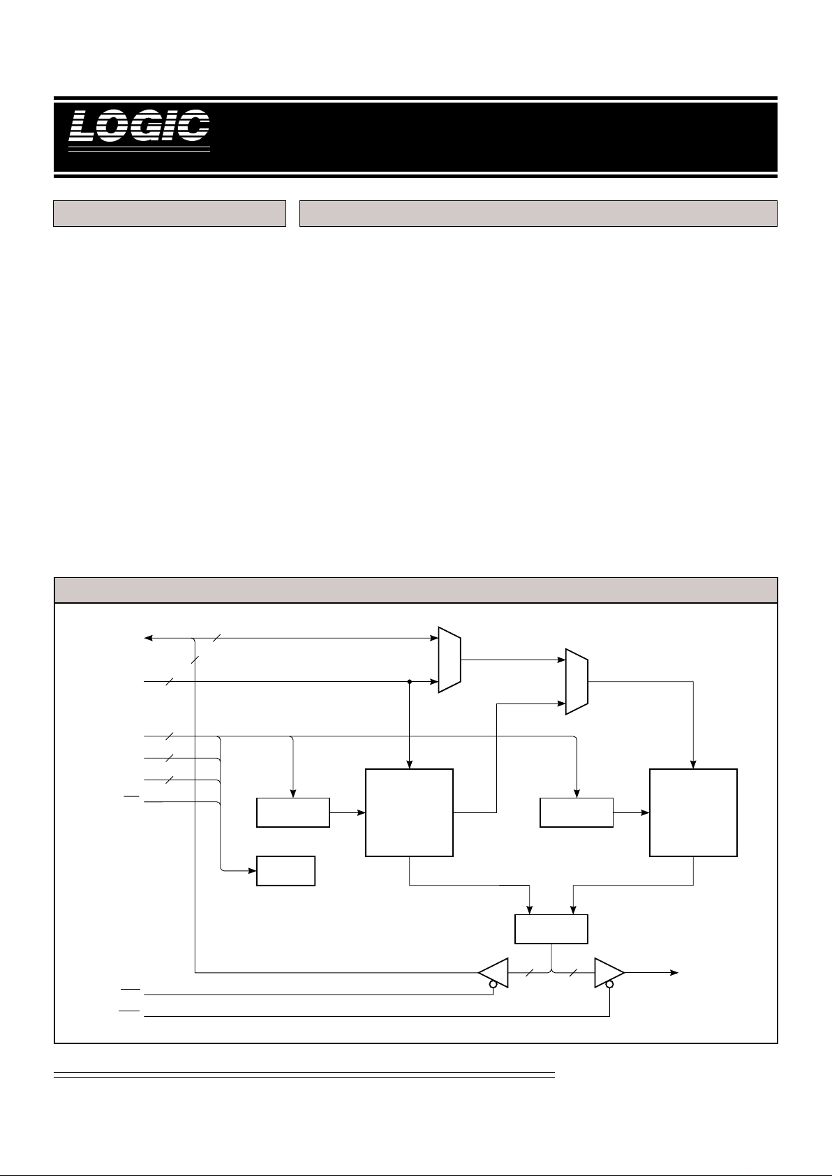
LF43168 BLOCK DIAGRAM
CIN
9-0
A
8-0
WR
CONTROL
10
9
CSEL
4-0
5
COEFFICIENT
BANK A
COEFFICIENT
BANK B
FILTER
CELL A
FILTER
CELL B
MUX
INA
9-0
INB
9-0
/
OUT
8-0
MUX/ADDER
9
19
MUX
OEL
OEH
OUT
27-9
10
10
9
Page 2
DEVICES INCORPORATED
LF43168
Dual 8-Tap FIR Filter
2
Video Imaging Products
03/28/2000–LDS.43168-H
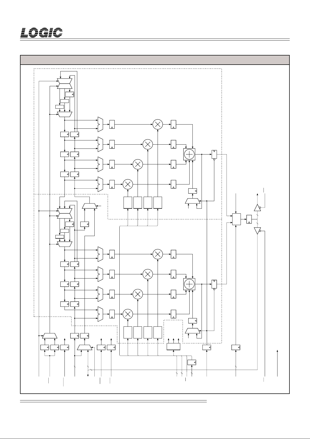
FIGURE 1. LF43168 FUNCTIONAL BLOCK DIAGRAM
TXFR
4
3
MUX
3
3
3
SHFTEN
INA
9-0
MUX
INB9-0/
OUT8-0
10
MUX_CTRL
TO ALL
DECIMATION
REGISTERS
CIN
9-0
A8-0
WR
CONTROL
COEF
BANK 0
COEF
BANK 1
COEF
BANK 2
COEF
BANK 3
3
FWRD
RVRS
TO ALL
ALUs
TO ALL
ALUs
ODD/EVEN
(TO ALL ALUs)
MUX_CTRL
ROUND_CTRL
3
ALU
1-16
1-16
1-16
1-16
1-16
1-16
MUX
0
MUX
MUX
DEMUX
10
9
1-16
MUX
MUX_CTRL
1-16
1-16
1-16
1-16
1-16
1-16
MUX
LIFO A
COEF
BANK 0
COEF
BANK 1
COEF
BANK 2
COEF
BANK 3
MUX
0
LIFO B
1-16
MUX
DEMUX
LIFO A
LIFO B
1-16
MUX_CTRL
5
ACCEN
MUX/
ADDER
ROUND_CTRL
6
MUX1-0
4
CSEL4-0
5
2
2
9 19
OUT27-9
OEL
OEH
CLK N data
CLK N+1 data
CLK N data
CLK N+1 data
10
AB
ALU
AB
ALU
AB
ALU
AB
ALU
AB
ALU
AB
ALU
AB
ALU
AB
FIR FILTER A FIR FILTER B
DECIMATION REGISTERS DECIMATION REGISTERS
NOTE: NUMBERS IN REGISTERS INDICATE NUMBER OF PIPELINE DELAYS.
CLK
9
Page 3
DEVICES INCORPORATED
Video Imaging Products
3
LF43168
Dual 8-Tap FIR Filter
03/28/2000–LDS.43168-H
SIGNAL DEFINITIONS
Power
VCC and GND
+5 V power supply. All pins must be
connected.
Clock
CLK — Master Clock
The rising edge of CLK strobes all
enabled registers.
Inputs
INA9-0 — Data Input (FIR Filter A)
INA9-0 is the 10-bit registered data
input port for FIR Filter A. INA9-0
can also be used to send data to FIR
Filter B. Data is latched on the
rising edge of CLK.
INB9-0 — Data Input (FIR Filter B)
INB9-0 is the 10-bit registered data
input port for FIR Filter B. Data is
latched on the rising edge of CLK.
INB9-1 is also used as OUT8-0, the nine
least significant bits of the data output
port (see OUT27-0 section).
CIN9-0 — Coefficient/Control Data Input
CIN9-0 is the data input port for the
coefficient and control registers. Data
is latched on the rising edge of WR.
A8-0 — Coefficient/Control Address
A8-0 provides the write address for data
on CIN9-0. Data is latched on the
falling edge of WR.
WR — Coefficient/Control Write
The rising edge of WR latches data on
CIN9-0 into the coefficient/control
register addressed by A8-0.
CSEL4-0 — Coefficient Select
CSEL4-0 determines which set of
coefficients is sent to the multipliers in
both FIR filters. Data is latched on the
rising edge of CLK.
Outputs
OUT27-0 — Data Output
OUT27-0 is the 28-bit registered data
output port. OUT8-0 is also used as
INB9-1, the nine most significant bits
of the FIR Filter B data input port (see
INB9-0 section). If both filters are
configured for even-symmetric
coefficients, and both input and
coefficient data is unsigned, the filter
output data will be unsigned. Otherwise, the output data will be in two’s
complement format.
Controls
SHFTEN — Shift Enable
When SHFTEN is LOW, data on
INA9-0 and INB9-0 can be latched into
the device and data can be shifted
through the decimation registers.
When SHFTEN is HIGH, data on
INA9-0 and INB9-0 can not be latched
into the device and data in the input
and decimation registers is held. This
signal is latched on the rising edge
of CLK.
FWRD — Forward ALU Input
When FWRD is LOW, data from the
forward decimation path is sent to the
“A” inputs on the ALUs. When
FWRD is HIGH, “0” is sent to the “A”
inputs on the ALUs. This signal is
latched on the rising edge of CLK.
RVRS — Reverse ALU Input
When RVRS is LOW, data from the
reverse decimation path is sent to the
“B” inputs on the ALUs. When RVRS
is HIGH, “0” is sent to the “B” inputs
on the ALUs. This signal is latched on
the rising edge of CLK.
TXFR — LIFO Transfer Control
When TXFR goes LOW, the LIFO
sending data to the reverse decimation
path becomes the LIFO receiving data
from the forward decimation path,
and the LIFO receiving data from the
forward decimation path becomes the
LIFO sending data to the reverse
decimation path. The device must see
a HIGH to LOW transition of TXFR in
order to switch LIFOs. This signal is
latched on the rising edge of CLK.
FIGURE 2A.INPUT FORMATS
987 210
2
02–12–2
2–72–82
–9
987 210
2
02–12–2
2–72–82
–9
987 210
–2
0
(Sign)
2–12
–2
2–72–82
–9
987 210
–2
0
(Sign)
2–12
–2
2–72–82
–9
Fractional Unsigned
Fractional Two's Complement
Data Coefficient
FIGURE 2B.OUTPUT FORMATS
27 26 25 2 1 0
2
92827
2
–162–172–18
27 26 25 2 1 0
–2
9
(Sign)
282
7
2
–162–172–18
Fractional Unsigned Fractional Two's Complement
Page 4
DEVICES INCORPORATED
LF43168
Dual 8-Tap FIR Filter
4
Video Imaging Products
03/28/2000–LDS.43168-H
ACCEN — Accumulate Enable
When ACCEN is HIGH, both accumulators are enabled for accumulation
and writing to the accumulator output
registers is disabled (the registers hold
their values). When ACCEN goes
LOW, accumulation is halted (by
sending zeros to the accumulator
feedback inputs) and writing to the
accumulator output registers is
enabled. This signal is latched on the
rising edge of CLK.
MUX1-0 — Mux/Adder Control
MUX1-0 controls the Mux/Adder as
shown in Table 3. Data is latched on
the rising edge of CLK.
OEL — Output Enable Low
When OEL is LOW, OUT8-0 is enabled
for output and INB9-1 can not be used.
When OEL is HIGH, OUT8-0 is placed
in a high-impedance state and INB9-1
is available for data input.
OEH — Output Enable High
When OEH is LOW, OUT27-9 is
enabled for output. When OEH is
HIGH, OUT27-9 is placed in a highimpedance state.
FUNCTIONAL DESCRIPTION
Control Registers
There are two control registers which
determine how the LF43168 is configured. Tables 1 and 2 show how each
register is organized. Data on CIN9-0
is latched into the addressed control
register on the rising edge of WR.
Address data is input on A8-0. Control Register 0 is written to using
address 000H. Control Register 1 is
written to using address 001H (Note
that addresses 002H to 0FFH are
reserved and should not be written
to). When a control register is written
to, a reset occurs which lasts for 6 CLK
cycles from when WR goes HIGH.
This reset does not alter any data in
the coefficient banks. Control data
can be loaded asynchronously to CLK.
Bits 0-3 of Control Register 0 control
the decimation registers. The decimation factor and decimation register
delay length is set using these bits.
Bit 4 determines if FIR filters A and B
operate separately as two filters or
together as one filter. Bit 5 is used to
select even or odd-symmetric coefficients. Bits 6 and 7 determine if there
are an even or odd number of taps in
filters A and B respectively. When the
FIR filters are set to operate as two
separate filters, bit 8 selects either
INA9-0 or INB9-0 as the filter B input
source. Bit 9 determines if the coefficient set used is interleaved or noninterleaved (see Interleaved Coefficient Filters section). Most applications use non-interleaved coefficient
sets (bit 9 set to “0”).
Bits 0 and 1 of Control Register 1
determine the input and coefficient
data formats respectively for filter A.
Bits 2 and 3 determine the input and
coefficient data formats respectively
for filter B. Bit 4 is used to enable or
disable data reversal on the reverse
decimation path. When data reversal
is enabled, the data order is reversed
before being sent to the reverse
decimation path. Bits 5-8 select where
rounding will occur on the output
data (See Mux/Adder section). Bit 9
enables or disables output rounding.
Coefficient Banks
The coefficient banks supply coefficient data to the multipliers in both
FIR filters. The LF43168 can store 32
different coefficient sets. A coefficient
BITS FUNCTION DESCRIPTION
0–3 Decimation Factor/ 0000 = No Decimation, Delay by 1
Decimation Register Delay Length 0001 = Decimate by 2, Delay by 2
0010 = Decimate by 3, Delay by 3
0011 = Decimate by 4, Delay by 4
0100 = Decimate by 5, Delay by 5
0101 = Decimate by 6, Delay by 6
0110 = Decimate by 7, Delay by 7
0111 = Decimate by 8, Delay by 8
1000 = Decimate by 9, Delay by 9
1001 = Decimate by 10, Delay by 10
1010 = Decimate by 11, Delay by 11
1011 = Decimate by 12, Delay by 12
1100 = Decimate by 13, Delay by 13
1101 = Decimate by 14, Delay by 14
1110 = Decimate by 15, Delay by 15
1111 = Decimate by 16, Delay by 16
4 Filter Mode Select 0 = Single Filter Mode
1 = Dual Filter Mode
5 Coefficient Symmetry Select 0 = Even-Symmetric Coefficients
1 = Odd-Symmetric Coefficients
6 FIR Filter A: Odd/Even Taps 0 = Odd Number of Filter Taps
1 = Even Number of Filter Taps
7 FIR Filter B: Odd/Even Taps 0 = Odd Number of Filter Taps
1 = Even Number of Filter Taps
8 FIR Filter B Input Source 0 = Input from INA9-0
1 = Input from INB9-0
9 Interleaved/Non-Interleaved 0 = Non-Interleaved Coefficient Sets
Coefficient Sets 1 = Interleaved Coefficient Sets
TABLE 1. CONTROL REGISTER 0 – ADDRESS 000H
Page 5
DEVICES INCORPORATED
Video Imaging Products
5
LF43168
Dual 8-Tap FIR Filter
03/28/2000–LDS.43168-H
set consists of 8 coefficient values.
Each bank can hold 32 10-bit values.
CSEL4-0 is used to select which
coefficient set is sent to the filter
multipliers. The coefficient set fed to
the multipliers may be switched every
CLK cycle if desired.
Data on CIN9-0 is latched into the
addressed coefficient bank on the
rising edge of WR. Address data is
input on A8-0 and is decoded as
follows: A1-0 determines the bank
number (“00”, “01”, “10”, and “11”
correspond to banks 0, 1, 2, and 3
respectively), A2 determines which
filter (“0” = filter A, “1” = filter B), A7-3
determines which set number the
coefficient is in, and A8 must be set to
“1”. For example, an address of
“100111011” will load coefficient set 7
in bank 3 of filter A with data. Coefficient data can be loaded asynchronously to CLK.
Decimation Registers
The decimation registers are provided
to take advantage of symmetric filter
coefficients and to provide data
storage for 2-D filtering. The outputs
of the registers are fed into the ALUs.
Both inputs to an ALU need to be
multiplied by the same filter coefficient. By adding or subtracting the
two data inputs together before being
sent to the filter multiplier, the number of filter taps needed is cut in half.
Therefore, an 8-tap FIR filter can be
made with only four multipliers. The
decimation registers are divided into
two groups, the forward and reverse
decimation registers. As can be seen
in Figure 1, data flows left to right
through the forward decimation
registers and right to left through the
reverse decimation registers. The
decimation registers can be pro-
BITS FUNCTION DESCRIPTION
0 FIR Filter A Input Data Format 0 = Unsigned
1 = Two’s Complement
1 FIR Filter A Coefficient Format 0 = Unsigned
1 = Two’s Complement
2 FIR Filter B Input Data Format 0 = Unsigned
1 = Two’s Complement
3 FIR Filter B Coefficient Format 0 = Unsigned
1 = Two’s Complement
4 Data Order Reversal Enable 0 = Enabled
1 = Disabled
5–8 Output Round Position 0000 = 2
–10
0001 = 2
–9
0010 = 2
–8
0011 = 2
–7
0100 = 2
–6
0101 = 2
–5
0110 = 2
–4
0111 = 2
–3
1000 = 2
–2
1001 = 2
–1
1010 = 2
0
1011 = 2
1
9 Output Round Enable 0 = Enabled
1 = Disabled
TABLE 2. CONTROL REGISTER 1 – ADDRESS 001H
grammed to decimate by 2 to 16 (see
Decimation section and Table 1).
SHFTEN enables and disables the
shifting of data through the decimation registers. When SHFTEN is LOW,
data on INA9-0 and INB9-0 can be
latched into the device and data can
be shifted through the decimation
registers. When SHFTEN is HIGH,
data on INA9-0 and INB9-0 can not be
latched into the device and data in the
input and decimation registers is held.
Data feedback circuitry is positioned
between the forward and reverse
decimation registers. It controls how
data from the forward decimation
path is fed to the reverse decimation
path. The feedback circuitry can
either reverse the data order or pass
the data unchanged to the reverse
decimation path. The mux/demux
sends incoming data to one of the
LIFOs or the data feedback decimation
register. The LIFOs and decimation
register feed into a mux. This mux
determines if one of the LIFOs or the
decimation register sends data to the
reverse decimation path.
If the data order needs to be reversed
before being sent to the reverse
decimation path (for example, when
decimating), Data Reversal Mode
should be enabled by setting bit 4 of
Control Register 1 to “0”. When Data
Reversal is enabled, data from the
forward decimation path is written
into one of the LIFOs in the data
feedback section while the other LIFO
sends data to the reverse decimation
path. When TXFR goes LOW, the
LIFO sending data to the reverse
decimation path becomes the LIFO
receiving data from the forward
decimation path, and the LIFO
receiving data from the forward
decimation path becomes the LIFO
sending data to the reverse decimation
path. The device must see a HIGH to
LOW transition of TXFR in order to
switch LIFOs. The size of data blocks
sent to the reverse decimation path is
determined by how often TXFR goes
LOW. To send data blocks of size 8 to
Page 6

DEVICES INCORPORATED
LF43168
Dual 8-Tap FIR Filter
6
Video Imaging Products
03/28/2000–LDS.43168-H
the reverse decimation path, TXFR
would have to be set LOW once every
8 CLK cycles. Once a data block size
has been established (by asserting
TXFR at the proper frequency),
changing the frequency or phase of
TXFR assertion will cause unknown
results.
If data should be passed to the reverse
decimation path with the order
unchanged, Data Reversal Mode
should be disabled by setting bit 4 of
Control Register 1 to “1” and TXFR
must be set LOW. When Data Reversal is disabled, data from the forward
decimation path is written into the
data feedback decimation register.
The output of this register sends data
to the reverse decimation path. The
delay length of this register is the
same as the forward and reverse
decimation register's delay length.
When the LF43168 is configured to
operate as a single FIR filter , the
forward and reverse decimation paths
in filters A and B are cascaded together .
The data feedback section in filter B
routes data from the forward decimation path to the reverse decimation
path. The configuration of filter B's
feedback section determines how data
is sent to the reverse decimation path.
Data going through the feedback
section in filter A is sent through the
decimation register.
The point at which data from the
forward decimation path is sent to the
data feedback section is determined
by whether the filter is set to have an
even or odd number of filter taps. If
the filter is set to have an even number
of taps, the output of the third forward decimation register is sent to the
feedback section. If the filter is set to
have an odd number of taps, the data
that will be output from the third
forward decimation register on the
next CLK cycle is sent to the feedback
section.
Accumulators
The multiplier outputs are fed into an
accumulator . Each filter has its own
accumulator . The accumulator can be
set to accumulate the multiplier
outputs or sum the multiplier outputs
and send the result to the accumulator
output register. When ACCEN is
HIGH, both accumulators are enabled
for accumulation and writing to the
accumulator output registers is
disabled (the registers hold their
values). When ACCEN goes LOW,
accumulation is halted (by sending
zeros to the accumulator feedback
inputs) and writing to the accumulator output registers is enabled.
Mux/Adder
When the LF43168 is configured as
two FIR filters, the Mux/Adder is
used to determine which filter drives
the output port. When the LF43168 is
configured as a single FIR filter, the
Mux/Adder is used to sum the
outputs of the two filters and send the
result to the output port. If 10-bit data
and 20-bit coefficients or 20-bit data
and 10-bit coefficients are requir ed,
the Mux/Adder can facilitate this by
scaling filter B’s output by 2
–10
before
being added to filter A’s output.
MUX1-0 determines what function the
Mux/Adder performs (see Table 3).
The Mux/Adder is also used to round
the output data before it is sent to the
output port. Output data is rounded by
adding a “1” to the bit position selected
using bits 5-8 of Control Register 1 (see
T able 2). For example, to r ound the
Decimation
Decimation by N is accomplished by
only reading the LF43168’s output once
every N clock cycles. For example, to
decimate by 10, the output should
only be read once every 10 clock
cycles. When not decimating, the
maximum number of taps possible
with a single filter in dual filter mode
is eight. When decimating by N, there
are N – 1 clock cycles between output
readings when the filter output is not
read. These extra clock cycles can be
used to calculate more filter taps. As
the decimation factor increases, the
number of available filter taps increases
also. When programmed to decimate
by N, the number of filter taps for a
single filter in dual filter mode increases
to 8N.
Arithmetic Logic Units
The ALUs can perform the following
operations: B + A, B – A, pass A, pass
B, and negate A (–A). If FWRD is
LOW, the forward decimation path
provides the A inputs to the ALUs. If
FWRD is HIGH, the A inputs are set to
"0". If RVRS is LOW, the reverse
decimation path provides the B inputs
to the ALUs. If RVRS is HIGH, the B
inputs are set to "0". FWRD, R VRS,
and the filter configuration determine
which ALU operation is performed. If
FWRD and RVRS are both set LOW,
and the filter is set for even-symmetric
coefficients, the ALU will perform the
B + A operation. If FWRD and RVRS
are both set LOW, and the filter is set
for odd-symmetric coefficients, the
ALU will perform the B – A operation.
If FWRD is set LOW, RVRS is set
HIGH, and the filter is set for evensymmetric coefficients, the ALU will
perform the pass A operation. If
FWRD is set LOW, RVRS is set HIGH,
and the filter is set for odd-symmetric
coefficients, the ALU will perform the
negate A operation. If FWRD is set
HIGH, RVRS is set LOW, and the filter
is set for either even or odd-symmetric
coefficients, the ALU will perform the
pass B operation.
MUX1-0 FUNCTION
00 Filter A + Filter B
(Filter B Scaled by 2
–10
)
01 Filter A + Filter B
10 Filter A
11 Filter B
TABLE 3. MUX1-0 FUNCTION
Page 7

DEVICES INCORPORATED
Video Imaging Products
7
LF43168
Dual 8-Tap FIR Filter
03/28/2000–LDS.43168-H
output to 16 bits, bits 5-8 of Control
Register 1 should be set to “0011”. This
will cause a “1” to be added to bit
position 2–7.
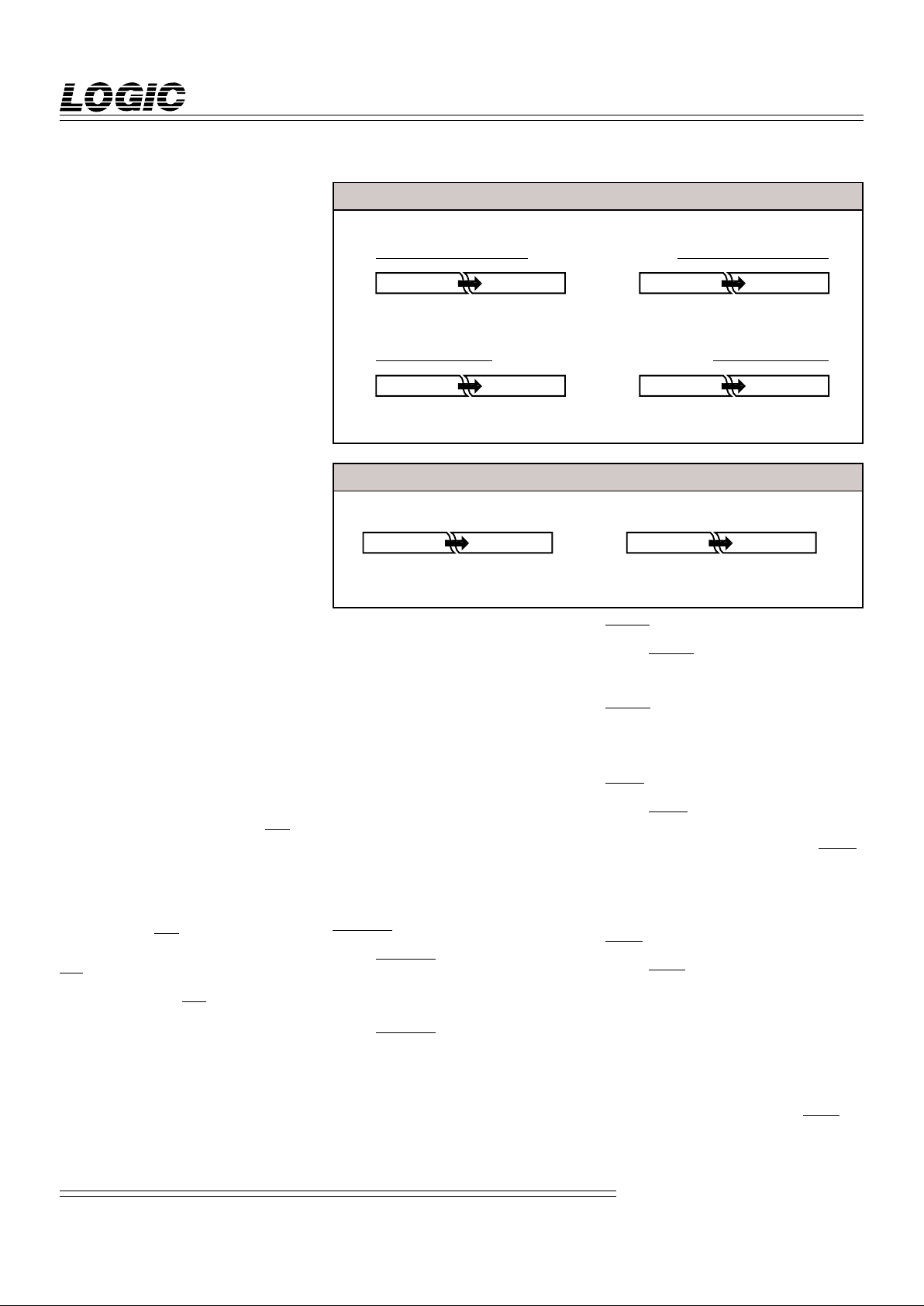
Symmetric Coefficients
The LF43168 filter architecture is
optimized for symmetric filter coefficient sets. Figure 3 shows examples of
the different types of symmetric
coefficient sets. In even-symmetric
sets, each coefficient value appears
twice (except in odd-tap sets where
the middle value appears only once).
In odd-symmetric sets, each coefficient
appears twice, but one value is
positive and one is negative. If the
two data input values that will be
multiplied by the same coefficient are
added or subtracted before being sent
to the filter multiplier , the number of
multipliers needed for an N-tap filter
is cut in half. Therefore, an 8-tap filter
can be implemented with four multipliers if a symmetric coefficient set is
used.
FIL TER CONFIGURA TIONS
Figures 4-6 show the data paths from
filter input to filter multipliers for all
symmetric coefficient filters. Figure 7
shows the interleaved coefficient filter
configuration. Each diagram shows
one of the two FIR filters when the
device is configured for dual filter
mode. The diagrams can be expanded
to include both filters when the device
is configured for single filter mode.
Even-Symmetric Coefficient Filters
Figure 4 shows the two possible
configurations when the device is
programmed for even-symmetric
coefficients and no decimation.
Note that coefficient 3 on the oddtap filter must be divided by two to
get the correct result (The coefficient
must be input to the device already
divided by two).
FIGURE 3. SYMMETRIC COEFFICIENT SET EXAMPLES
12345678
Even-Tap, Even-Symmetric
Coefficient Set
Odd-Tap, Even-Symmetric
Coefficient Set
1234
5678
Even-Tap, Odd-Symmetric
Coefficient Set
1234567
FIGURE 4. EVEN-SYMMETRIC COEFFICIENT FILTER CONFIGURATIONS (NO DECIMATION)
COEF 0
COEF 1
COEF 2
COEF 3
B + A
AB
B + A
AB
B + A
AB
B + A
AB
DATA IN
EVEN-TAP FILTER
COEF 0
COEF 1
COEF 2
COEF 3
B + A
AB
B + A
AB
B + A
AB
B + A
AB
DATA IN
2
ODD-TAP FILTER
Page 8

DEVICES INCORPORATED
LF43168
Dual 8-Tap FIR Filter
8
Video Imaging Products
03/28/2000–LDS.43168-H
Figure 5 shows the two possible
configurations when the device is
programmed as a decimating, evensymmetric coefficient filter. The delay
length of the decimation registers will
be equal to the decimation factor that
the device is programmed for. Since
only four coefficients (effectively
eight) can be sent to the filter multipli-
ers on a clock cycle, it may be necessary (depending on the coefficient set)
to change the coefficients fed to the
multipliers on different CLK cycles for
filters with more than eight taps. Note
that for the odd-tap filter , the middle
coefficient of the coefficient set must
be divided by two to get the correct
result.
Odd-Symmetric Coefficient Filters
Figure 6 shows the two possible
configurations when the device is
programmed for odd-symmetric
coefficients. Note that odd-tap, oddsymmetric coefficient filters are not
possible.
FIGURE 5. DECIMATING, EVEN-SYMMETRIC COEFFICIENT FILTER CONFIGURATIONS
COEF 0
COEF 1
COEF 2
COEF 3
B + A
AB
B + A
AB
B + A
AB
B + A
AB
DATA IN
MUX
LIFO ALIFO B
DEMUX
NNN
NNN
N = Delay Length (Decimation Factor)
EVEN-TAP FILTER
COEF 0
COEF 1
COEF 2
COEF 3
B + A
AB
B + A
AB
B + A
AB
B + A
AB
DATA IN
MUX
LIFO ALIFO B
DEMUX
NNN
NNN
N = Delay Length (Decimation Factor)
Delay Stage N – 1 Output
ODD-TAP FILTER
FIGURE 6. ODD-SYMMETRIC COEFFICIENT FILTER CONFIGURATIONS
COEF 0
COEF 1
COEF 2
COEF 3
B – A
AB
B – A
AB
B – A
AB
B – A
AB
DATA IN
EVEN-TAP FILTER (NO DECIMATION
)
COEF 0
COEF 1
COEF 2
COEF 3
B – A
AB
B – A
AB
B – A
AB
B – A
AB
DATA IN
MUX
LIFO ALIFO B
DEMUX
NNN
NNN
N = Delay Length (Decimation Factor)
DECIMATING, EVEN-TAP FILTER
Page 9

DEVICES INCORPORATED
Video Imaging Products
9
LF43168
Dual 8-Tap FIR Filter
03/28/2000–LDS.43168-H
Interleaved Coefficient Filters
Figure 7 shows the filter configuration
when the device is programmed for
interleaved coefficients. An inter leaved coefficient set contains two
separate odd-tap, even-symmetric
coefficient sets which have been
interleaved together (see Figure 8). If
two data sets are interleaved into the
same serial data stream, they can both
be filtered by different coef ficient sets
if the two coefficient sets are also
interleaved. The LF43168 is configured as an interleaved coefficient filter
by programming the device for
interleaved coefficient sets, evensymmetric coefficients, odd number of
filter taps, and data reversal disabled.
Note that coefficient 3, in Figure 7,
must be divided by two to get the
correct result.
Asymmetric Coefficient Filters
It is possible to have asymmetric
coefficient filters. Asymmetric coef ficient sets do not exhibit even or odd
symmetric properties. A 4-tap asymmetric filter is possible by putting the
device in even-tap, pass A mode and
then feeding the asymmetric coefficient set to the multipliers. An 8-tap
asymmetric filter is possible if the
device is clocked twice as fast as the
input data rate. It will take two CLK
cycles to calculate the output. On the
first CLK cycle, the reverse decimation
path is selected to feed data to the
filter multipliers. On the second CLK
cycle, the coefficients sent to the
multipliers are changed (if necessary)
and the forward decimation path is
selected to feed data to the filter
multipliers.
FIGURE 8. INTERLEAVED COEFFICIENT SET EXAMPLE
Interleaved Coefficient Set
Consisting of Sets A and B
12345
678910
12345
Odd-Tap, Even-Symmetric
Coefficient Set B
12345
Odd-Tap, Even-Symmetric
Coefficient Set A
67
67
11121314
FIGURE 7. INTERLEAVED COEFFICIENT FILTER CONFIGURATION
COEF 0
COEF 1
COEF 2
B + A
AB
B + A
AB
B + A
AB
B + A
AB
DATA IN
ODD-TAP INTERLEAVED FILTER
NNN
NNN
N = Delay Length (Decimation Factor)
N
COEF 3
2
Page 10

DEVICES INCORPORATED
LF43168
Dual 8-Tap FIR Filter
10
Video Imaging Products
03/28/2000–LDS.43168-H
Storage temperature ........................................................................................................... –65°C to +150°C
Operating ambient temperature........................................................................................... –55°C to +125°C
VCC supply voltage with respect to ground............................................................................ –0.5V to +7.0V
Input signal with respect to ground ............................................................................... –0.5 V to VCC + 0.5 V
Signal applied to high impedance output ...................................................................... –0.5 V to VCC + 0.5 V
Output current into low outputs............................................................................................................. 25 mA
Latchup current ............................................................................................................................... > 400 mA
MAXIMUM RATINGS
Above which useful life may be impaired (Notes 1, 2, 3, 8)
OPERATING CONDITIONS
To meet specified electrical and switching characteristics
Mode Temperature Range (Ambient) Supply Voltage
Active Operation, Commercial 0°C to +70°C 4.75 V ≤ VCC ≤ 5.25 V
Active Operation, Military –55°C to +125°C 4.50V ≤ VCC ≤ 5.50 V
Symbol Parameter Test Condition Min Typ Max Unit
VOH Output High Voltage VCC = Min., IOH = –2.0 mA 2.6 V
VOL Output Low Voltage VCC = Min., IOL = 4.0 mA 0.4 V
VIH Input High Voltage 2.0 VCC V
VIL Input Low Voltage (Note 3) 0.0 0.8 V
IIX Input Current Ground ≤ VIN ≤ VCC (Note 12) ±10 µA
IOZ Output Leakage Current Ground ≤ VOUT ≤ VCC (Note 12) ±10 µA
ICC1 VCC Current, Dynamic (Notes 5, 6) 300 mA
ICC2 VCC Current, Quiescent (Note 7) 500 µA
CIN Input Capacitance TA = 25°C, f = 1 MHz 12 pF
COUT Output Capacitance TA = 25°C, f = 1 MHz 12 pF
ELECTRICAL CHARACTERISTICS
Over Operating Conditions (Note 4)
Page 11

DEVICES INCORPORATED
Video Imaging Products
11
LF43168
Dual 8-Tap FIR Filter
03/28/2000–LDS.43168-H
LF43168–
30 22 15
Symbol Parameter Min Max Min Max Min Max
tCYC Cycle Time 30 22 15
tPW Clock Pulse Width 12 8 7
tS Input Setup Time 15 12 5
tH Input Hold Time 0 0 0
tWP Write Period 30 22 15
tWPW Write Pulse Width 12 10 7
tWHCH Write High to Clock High 5 3 2
tCWS CIN9-0 Setup Time 12 10 5
tCWH CIN9-0 Hold Time 0 0 0
tAWS Address Setup Time 1 0 8 5
tAWH Address Hold Time 0 0 0
tD Output Delay 14 12 11
tENA Three-State Output Enable Delay (Note 11) 12 12 12
tDIS Three-State Output Disable Delay (Note 11) 12 12 12
COMMERCIAL OPERATING RANGE
Notes 9, 10 (ns)
SWITCHING CHARACTERISTICS
SWITCHING WAVEFORMS
CLK
INPUTS/
CIN
9-0
t
PW
t
PW
t
CYC
A
8-0
OEL
OUT
27-0
t
H
t
S
t
D
t
DIS
HIGH IMPEDANCE
t
ENA
OEH
WR
t
AWS
t
AWH
t
CWH
t
CWS
t
WHCH
*includes INA
9-0
, INB
9-0
, CSEL
4-0
, ACCEN, MUX
1-0
, SHFTEN, FWRD, RVRS, and TXFR.
CONTROLS*
t
WPW
t
WPW
t
WP
Page 12

DEVICES INCORPORATED
LF43168
Dual 8-Tap FIR Filter
12
Video Imaging Products
03/28/2000–LDS.43168-H
1234567890123456789012345678901212345678901234
1
23456789012345678901234567890121234567890123
4
1
23456789012345678901234567890121234567890123
4
1
23456789012345678901234567890121234567890123
4
1
23456789012345678901234567890121234567890123
4
1
23456789012345678901234567890121234567890123
4
1
23456789012345678901234567890121234567890123
4
1
23456789012345678901234567890121234567890123
4
1
23456789012345678901234567890121234567890123
4
1
23456789012345678901234567890121234567890123
4
1
23456789012345678901234567890121234567890123
4
1
23456789012345678901234567890121234567890123
4
1
23456789012345678901234567890121234567890123
4
1
23456789012345678901234567890121234567890123
4
1
23456789012345678901234567890121234567890123
4
1
23456789012345678901234567890121234567890123
4
1
23456789012345678901234567890121234567890123
4
1
23456789012345678901234567890121234567890123
4
1
23456789012345678901234567890121234567890123
4
1
23456789012345678901234567890121234567890123
4
1
23456789012345678901234567890121234567890123
4
1
23456789012345678901234567890121234567890123
4
1
23456789012345678901234567890121234567890123
4
1
23456789012345678901234567890121234567890123
4
1
23456789012345678901234567890121234567890123
4
1
23456789012345678901234567890121234567890123
4
1
23456789012345678901234567890121234567890123
4
1
23456789012345678901234567890121234567890123
4
1
23456789012345678901234567890121234567890123
4
1
23456789012345678901234567890121234567890123
4
1
23456789012345678901234567890121234567890123
4
1
23456789012345678901234567890121234567890123
4
1
23456789012345678901234567890121234567890123
4
1
23456789012345678901234567890121234567890123
4
1
23456789012345678901234567890121234567890123
4
1
23456789012345678901234567890121234567890123
4
1
23456789012345678901234567890121234567890123
4
1
23456789012345678901234567890121234567890123
4
1
23456789012345678901234567890121234567890123
4
1
23456789012345678901234567890121234567890123
4
1
23456789012345678901234567890121234567890123
4
1
23456789012345678901234567890121234567890123
4
1
23456789012345678901234567890121234567890123
4
1
23456789012345678901234567890121234567890123
4
1
23456789012345678901234567890121234567890123
4
1
23456789012345678901234567890121234567890123
4
1
23456789012345678901234567890121234567890123
4
1
23456789012345678901234567890121234567890123
4
1
23456789012345678901234567890121234567890123
4
1
23456789012345678901234567890121234567890123
4
1234567890123456789012345678901212345678901234
LF43168–
39
*
30
*
22
*
Symbol Parameter Min Max Min Max Min Max
tCYC Cycle Time 39 30 22
tPW Clock Pulse Width 15 12 8
tS Input Setup Time 17 15 12
tH Input Hold Time 0 0 0
tWP Write Period 39 30 22
tWPW Write Pulse Width 15 12 10
tWHCH Write High to Clock High 8 5 3
tCWS CIN9-0 Setup Time 15 12 10
tCWH CIN9-0 Hold Time 0 0 0
tAWS Address Setup Time 1 0 10 8
tAWH Address Hold Time 0 0 0
tD Output Delay 17 15 12
tENA Three-State Output Enable Delay (Note 11) 12 12 12
tDIS Three-State Output Disable Delay (Note 11) 12 12 12
MILITARY OPERATING RANGE
Notes 9, 10 (ns)
SWITCHING CHARACTERISTICS
SWITCHING WAVEFORMS
CLK
INPUTS/
CIN
9-0
t
PW
t
PW
t
CYC
A
8-0
OEL
OUT
27-0
t
H
t
S
t
D
t
DIS
HIGH IMPEDANCE
t
ENA
OEH
WR
t
AWS
t
AWH
t
CWH
t
CWS
t
WHCH
*includes INA
9-0
, INB
9-0
, CSEL
4-0
, ACCEN, MUX
1-0
, SHFTEN, FWRD, RVRS, and TXFR.
CONTROLS*
t
WPW
t
WPW
t
WP
*DISCONTINUED SPEED GRADE
Page 13

DEVICES INCORPORATED
Video Imaging Products
13
LF43168
Dual 8-Tap FIR Filter
03/28/2000–LDS.43168-H
1. Maximum Ratings indicate stress
specifications only. Functional operation of these products at values beyond
those indicated in the Operating Conditions table is not implied. Exposure to
maximum rating conditions for extended periods may affect reliability.
2. The products described by this specification include internal circuitry designed to protect the chip from damaging substrate injection currents and accumulations of static charge. Nevertheless, conventional precautions should
be observed during storage, handling,
and use of these circuits in order to
avoid exposure to excessive electrical
stress values.
3. This device provides hard clamping of
transient undershoot and overshoot. Input levels below ground or above VCC
will be clamped beginning at –0.6 V and
VCC + 0.6 V. The device can withstand
indefinite operation with inputs in the
range of –0.5 V to +7.0 V. Device operation will not be adversely affected, however, input current levels will be well in
excess of 100 mA.
4. Actual test conditions may vary from
those designated but operation is guaranteed as specified.
5. Supply current for a given application can be accurately approximated by:
where
N = total number of device outputs
C = capacitive load per output
V = supply voltage
F = clock frequency
6. Tested with all outputs changing every cycle and no load, at a 20 MHz clock
rate.
7. Tested with all inputs within 0.1 V of
VCC or Ground, no load.
8. These parameters are guaranteed
but not 100% tested.
NCV F
4
2
NOTES
9. AC specifications are tested with
input transition times less than 3 ns,
output reference levels of 1.5 V (except
tDIS test), and input levels of nominally
0 to 3.0 V. Output loading may be a
resistive divider which provides for
specified IOH and IOL at an output
voltage of VOH min and VOL max
respectively. Alternatively, a diode
bridge with upper and lower current
sources of IOH and IOL respectively,
and a balancing voltage of 1.5 V may be
used. Parasitic capacitance is 30 pF
minimum, and may be distributed.
This device has high-speed outputs capable of large instantaneous current
pulses and fast turn-on/turn-off times.
As a result, care must be exercised in the
testing of this device. The following
measures are recommended:
a. A 0.1 µF ceramic capacitor should be
installed between VCC and Ground
leads as close to the Device Under Test
(DUT) as possible. Similar capacitors
should be installed between device VCC
and the tester common, and device
ground and tester common.
b. Ground and VCC supply planes
must be brought directly to the DUT
socket or contactor fingers.
c. Input voltages should be adjusted to
compensate for inductive ground and VCC
noise to maintain required DUT input
levels relative to the DUT ground pin.
10. Each parameter is shown as a minimum or maximum value. Input requirements are specified from the point
of view of the external system driving
the chip. Setup time, for example, is
specified as a minimum since the external system must supply at least that
much time to meet the worst-case requirements of all parts. Responses from
the internal circuitry are specified from
the point of view of the device. Output
delay, for example, is specified as a
maximum since worst-case operation of
any device always provides data within
that time.
11. For the tENA test, the transition is
measured to the 1.5 V crossing point
with datasheet loads. For the tDIS test,
the transition is measured to the
±200mV level from the measured
steady-state output voltage with
±10mA loads. The balancing voltage, VTH, is set at 3.5 V for Z-to-0
and 0-to-Z tests, and set at 0 V for Zto-1 and 1-to-Z tests.
12. These parameters are only tested at
the high temperature extreme, which is
the worst case for leakage current.
S1
I
OH
I
OL
V
TH
C
L
DUT
OE
0.2 V
t
DIS
t
ENA
0.2 V
1.5 V 1.5 V
3.5V Vth
1
Z
0
Z
Z
1
Z
0
1.5 V
1.5 V
0V Vth
VOL*
V
OH
*
V
OL
*
V
OH
*
Measured V
OL
with IOH = –10mA and IOL = 10mA
Measured V
OH
with IOH = –10mA and IOL = 10mA
FIGURE B. THRESHOLD LEVELS
FIGURE A. OUTPUT LOADING CIRCUIT
Page 14

DEVICES INCORPORATED
LF43168
Dual 8-Tap FIR Filter
14
Video Imaging Products
03/28/2000–LDS.43168-H
Plastic J-Lead Chip Carrier
(J3)
LF43168JC30
LF43168JC22
LF43168JC15
84-pin
Speed
30 ns
22 ns
15 ns
ORDERING INFORMATION
1234567
74
73
72
71
70
69
68
67
66
65
64
63
62
61
60
59
58
57
56
55
54
84 83 82 81 80 79
4443 45 46 47 493837 39 40 41 42
12
13
14
15
16
17
18
19
20
21
22
23
24
25
26
27
28
29
30
31
32
48
Top
View
891011 78 77 76 75
36353433 50 51 52 53
CIN
7
CIN
6
CIN
5
CIN
4
GND
CIN
3
CIN
2
CIN
1
CIN
0
INA
9
INA
8
INA
7
INA
6
INA
5
V
CC
INA
4
INA
3
INA
2
INA
1
INA
0
INB
9
RVRS
FWRD
SHFTEN
TXFR
ACCEN
V
CC
CLK
GND
OEH
OUT
27
OUT
26
OUT
25
OUT
24
OUT
23
OUT
22
OUT
21
OUT
20
OUT
19
OUT
18
OUT
17
V
CC
INB8INB7INB6INB
5
GND
INB
4
INB3INB2INB1INB
0
OEL
OUT
9
OUT
10
V
CC
OUT11OUT12OUT13OUT14OUT15OUT
16
GND
CIN
8
CIN9CSEL4CSEL3CSEL2CSEL1CSEL0VCCA8A7A6A5A4A3A2A1A0GNDWRMUX1MUX
0
–40°C to +85°C — COMMERCIAL SCREENING
0°C to +70°C — COMMERCIAL SCREENING
Page 15

DEVICES INCORPORATED
Video Imaging Products
15
LF43168
Dual 8-Tap FIR Filter
03/28/2000–LDS.43168-H
Plastic Quad Flatpack
(Q2)
LF43168QC30
LF43168QC22
LF43168QC15
100-pin
Speed
30 ns
22 ns
15 ns
ORDERING INFORMATION
CIN8
NC
CIN7
NC
CIN6
CIN5
CIN4
GND
GND
CIN3
CIN2
CIN1
CIN0
INA9
INA8
INA7
INA6
INA5
VCC
VCC
INA4
INA3
INA2
INA1
INA0
NC
NC
INB9
INB8
INB7
CIN9
CSEL4
CSEL3
CSEL2
CSEL1
CSEL0
VCC
VCCA8A7A6A5A4A3A2A1A0GND
GND
WR
MUX1
MUX0
RVRS
NC
FWRD
SHFTEN
TXFR
ACCEN
VCC
VCC
CLK
GND
GND
OEH
OUT27
OUT26
OUT25
OUT24
OUT23
OUT22
OUT21
OUT20
OUT19
OUT18
OUT17
NC
VCC
VCC
GND
GND
INB6
INB5
GND
GND
INB
4
INB3
INB2
INB1
INB0
OEL
OUT9
OUT10
VCC
VCC
OUT11
OUT12
OUT13
OUT14
OUT15
OUT16
80
79
78
77
76
75
74
73
72
71
70
69
68
67
66
65
64
63
62
61
60
59
58
57
56
55
54
53
52
51
Top
View
1
2
3
4
5
6
7
8
9
10
11
12
13
14
15
16
17
18
19
20
21
22
23
24
25
26
27
28
29
30
31323334353637383940414243444546474849
50
100
99989796959493929190898887868584838281
–40°C to +85°C — COMMERCIAL SCREENING
0°C to +70°C — COMMERCIAL SCREENING
Page 16

DEVICES INCORPORATED
LF43168
Dual 8-Tap FIR Filter
16
Video Imaging Products
03/28/2000–LDS.43168-H
23456789012345678901234567890121234567890123456789012345678901212345678901234567890123456789012
1
23456789012345678901234567890121234567890123456789012345678901212345678901234567890123456789012
1
23456789012345678901234567890121234567890123456789012345678901212345678901234567890123456789012
1
23456789012345678901234567890121234567890123456789012345678901212345678901234567890123456789012
1
23456789012345678901234567890121234567890123456789012345678901212345678901234567890123456789012
1
23456789012345678901234567890121234567890123456789012345678901212345678901234567890123456789012
1
23456789012345678901234567890121234567890123456789012345678901212345678901234567890123456789012
1
23456789012345678901234567890121234567890123456789012345678901212345678901234567890123456789012
1
23456789012345678901234567890121234567890123456789012345678901212345678901234567890123456789012
1
23456789012345678901234567890121234567890123456789012345678901212345678901234567890123456789012
1
23456789012345678901234567890121234567890123456789012345678901212345678901234567890123456789012
1
23456789012345678901234567890121234567890123456789012345678901212345678901234567890123456789012
1
23456789012345678901234567890121234567890123456789012345678901212345678901234567890123456789012
1
23456789012345678901234567890121234567890123456789012345678901212345678901234567890123456789012
1
23456789012345678901234567890121234567890123456789012345678901212345678901234567890123456789012
1
23456789012345678901234567890121234567890123456789012345678901212345678901234567890123456789012
1
23456789012345678901234567890121234567890123456789012345678901212345678901234567890123456789012
1
23456789012345678901234567890121234567890123456789012345678901212345678901234567890123456789012
1
23456789012345678901234567890121234567890123456789012345678901212345678901234567890123456789012
1
23456789012345678901234567890121234567890123456789012345678901212345678901234567890123456789012
1
23456789012345678901234567890121234567890123456789012345678901212345678901234567890123456789012
1
23456789012345678901234567890121234567890123456789012345678901212345678901234567890123456789012
1
23456789012345678901234567890121234567890123456789012345678901212345678901234567890123456789012
1
23456789012345678901234567890121234567890123456789012345678901212345678901234567890123456789012
1
23456789012345678901234567890121234567890123456789012345678901212345678901234567890123456789012
1
23456789012345678901234567890121234567890123456789012345678901212345678901234567890123456789012
1
23456789012345678901234567890121234567890123456789012345678901212345678901234567890123456789012
1
23456789012345678901234567890121234567890123456789012345678901212345678901234567890123456789012
1
23456789012345678901234567890121234567890123456789012345678901212345678901234567890123456789012
1
23456789012345678901234567890121234567890123456789012345678901212345678901234567890123456789012
1
23456789012345678901234567890121234567890123456789012345678901212345678901234567890123456789012
1
23456789012345678901234567890121234567890123456789012345678901212345678901234567890123456789012
1
23456789012345678901234567890121234567890123456789012345678901212345678901234567890123456789012
1
23456789012345678901234567890121234567890123456789012345678901212345678901234567890123456789012
1
23456789012345678901234567890121234567890123456789012345678901212345678901234567890123456789012
1
23456789012345678901234567890121234567890123456789012345678901212345678901234567890123456789012
1
23456789012345678901234567890121234567890123456789012345678901212345678901234567890123456789012
1
23456789012345678901234567890121234567890123456789012345678901212345678901234567890123456789012
1
23456789012345678901234567890121234567890123456789012345678901212345678901234567890123456789012
1
23456789012345678901234567890121234567890123456789012345678901212345678901234567890123456789012
1
23456789012345678901234567890121234567890123456789012345678901212345678901234567890123456789012
1
23456789012345678901234567890121234567890123456789012345678901212345678901234567890123456789012
1
23456789012345678901234567890121234567890123456789012345678901212345678901234567890123456789012
1
23456789012345678901234567890121234567890123456789012345678901212345678901234567890123456789012
1
23456789012345678901234567890121234567890123456789012345678901212345678901234567890123456789012
1
23456789012345678901234567890121234567890123456789012345678901212345678901234567890123456789012
1
23456789012345678901234567890121234567890123456789012345678901212345678901234567890123456789012
1
23456789012345678901234567890121234567890123456789012345678901212345678901234567890123456789012
1
23456789012345678901234567890121234567890123456789012345678901212345678901234567890123456789012
1
23456789012345678901234567890121234567890123456789012345678901212345678901234567890123456789012
1
23456789012345678901234567890121234567890123456789012345678901212345678901234567890123456789012
1
23456789012345678901234567890121234567890123456789012345678901212345678901234567890123456789012
1
23456789012345678901234567890121234567890123456789012345678901212345678901234567890123456789012
1
23456789012345678901234567890121234567890123456789012345678901212345678901234567890123456789012
1
23456789012345678901234567890121234567890123456789012345678901212345678901234567890123456789012
1
23456789012345678901234567890121234567890123456789012345678901212345678901234567890123456789012
1
23456789012345678901234567890121234567890123456789012345678901212345678901234567890123456789012
1
23456789012345678901234567890121234567890123456789012345678901212345678901234567890123456789012
1
23456789012345678901234567890121234567890123456789012345678901212345678901234567890123456789012
1
23456789012345678901234567890121234567890123456789012345678901212345678901234567890123456789012
1
23456789012345678901234567890121234567890123456789012345678901212345678901234567890123456789012
1
23456789012345678901234567890121234567890123456789012345678901212345678901234567890123456789012
1
23456789012345678901234567890121234567890123456789012345678901212345678901234567890123456789012
1
23456789012345678901234567890121234567890123456789012345678901212345678901234567890123456789012
1
23456789012345678901234567890121234567890123456789012345678901212345678901234567890123456789012
1
23456789012345678901234567890121234567890123456789012345678901212345678901234567890123456789012
1
23456789012345678901234567890121234567890123456789012345678901212345678901234567890123456789012
1
Ceramic Pin Grid Array
(G6)
84-pin
Speed
ORDERING INFORMATION
0°C to +70°C — COMMERCIAL SCREENING
–55°C to +125°C — MIL-STD-883 COMPLIANT
–55°C to +125°C — COMMERCIAL SCREENING
A
B
C
D
E
F
G
H
J
K
L
Top View
Through Package
(i.e., Component Side Pinout)
12345
6
7 8 9 10 11
CSEL
4
CIN
7
CIN
6
GND
CIN
1
INA
9
INA
5
INA
3
INA
0
INB
8
INB
6
CSEL
3
CIN
9
CIN
2
INA
8
INA
7
INB
7
INB
5
CSEL
1
CSEL
2
GND
INB
4
A
8
V
CC
CSEL
0
INB
3
INB
2
INB
1
A
7
A
2
A
6
OEL
INB
0
OUT
11
A
4
A
3
A
5
OUT
9
V
CC
OUT
10
A
1
A
0
OUT
13
OUT
12
CIN
8
CIN
5
CIN
4
CIN
3
CIN
0
V
CC
INA
6
INA
4
INA
2
INA
1
INB
9
GND
MUX
1
CLK
OUT
26
OUT
25
OUT
16
OUT
14
WR
MUX
0
FWRD
ACCEN
GND
OUT
22
OUT
23
OUT
20
OUT
17
V
CC
OUT
15
RVRS
SHFTEN
TXFR
V
CC
OEH
OUT
27
OUT
24
OUT
21
OUT
19
OUT
18
GND
Discontinued Package
 Loading...