

Page 1
LF198/LF298/LF398, LF198A/LF398A
Monolithic Sample-and-Hold Circuits
LF198/LF298/LF398, LF198A/LF398A Monolithic Sample-and-Hold Circuits
May 1998
General Description
The LF198/LF298/LF398 are monolithic sample-and-hold
circuits which utilize BI-FET technology to obtain ultra-high
dc accuracy with fast acquisition of signal and low droop
rate. Operating as a unity gain follower, dc gain accuracy is
0.002%typical and acquisition time is as low as 6 µs to
0.01%. A bipolar input stage is used to achieve low offset
voltage and wide bandwidth. Input offset adjust is accomplished with a single pin, and does not degrade input offset
drift. The widebandwidthallowstheLF198 to be included inside the feedback loop of 1 MHz op amps without having stability problems. Input impedance of 10
source impedances to be used without degrading accuracy.
P-channel junction FET’s are combined with bipolar devices
in the output amplifier to give droop rates as low as 5 mV/min
witha1µFhold capacitor. The JFET’s have much lower
noise than MOS devices used in previous designs and do
not exhibit high temperature instabilities. The overall design
guarantees no feed-through from input to output in the hold
mode, even for input signals equal to the supply voltages.
10
Ω allows high
Features
n Operates from±5V to±18V supplies
n Less than 10 µs acquisition time
n TTL, PMOS, CMOS compatible logic input
n 0.5 mV typical hold step at C
n Low input offset
n 0.002%gain accuracy
n Low output noise in hold mode
n Input characteristics do not change during hold mode
n High supply rejection ratio in sample or hold
n Wide bandwidth
n Space qualified
Logic inputs on the LF198 are fully differential with low input
current, allowing direct connection to TTL, PMOS, and
CMOS. Differential threshold is 1.4V. The LF198 will operate
±
from
5V to±18V supplies.
An “A” version is available with tightened electrical
specifications.
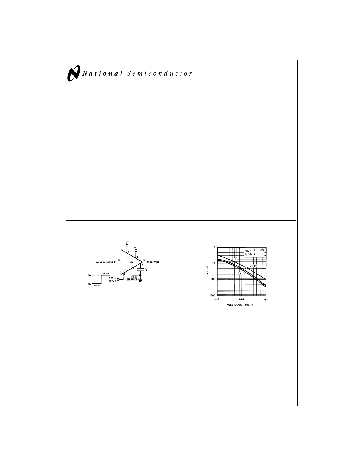
Typical Connection and Performance Curve
=
h
Acquisition Time
0.01 µF
DS005692-32
DS005692-16
© 1999 National Semiconductor Corporation DS005692 www.national.com
Page 2
Absolute Maximum Ratings (Note 1)
If Military/Aerospace specified devices are required,
please contact the National Semiconductor Sales Office/
Distributors for availability and specifications.
Supply Voltage
Power Dissipation (Package
Limitation) (Note 2) 500 mW
Operating Ambient Temperature Range
LF198/LF198A −55˚C to +125˚C
LF298 −25˚C to +85˚C
LF398/LF398A 0˚C to +70˚C
Storage Temperature Range −65˚C to +150˚C
Input Voltage Equal to Supply Voltage
Logic To Logic Reference
Differential Voltage (Note 3) +7V, −30V
Output Short Circuit Duration Indefinite
±
18V
Hold Capacitor Short
Circuit Duration 10 sec
Lead Temperature (Note 4)
H package (Soldering, 10 sec.) 260˚C
N package (Soldering, 10 sec.) 260˚C
M package:
Vapor Phase (60 sec.) 215˚C
Infrared (15 sec.) 220˚C
Thermal Resistance (θ
) (typicals)
JA
H package 215˚C/W (Board mount in still air)
85˚C/W (Board mount in
400LF/min air flow)
N package 115˚C/W
M package 106˚C/W
(H package, typical) 20˚C/W
θ
JC
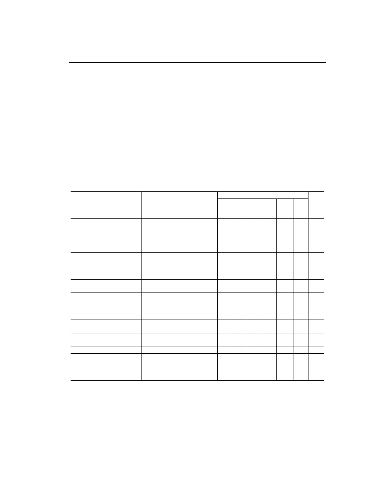
Electrical Characteristics
The following specifcations apply for −VS+ 3.5V ≤ VIN≤ +VS− 3.5V, +V
=
R
10 kΩ, LOGIC REFERENCE=0V, LOGIC HIGH=2.5V, LOGIC LOW=0V unless otherwise specified.
L
=
S
+15V, −V
Parameter Conditions LF198/LF298 LF398 Units
Min Typ Max Min Typ Max
=
Input Offset Voltage, (Note 5) T
25˚C 1 3 2 7 mV
j
Full Temperature Range 5 10 mV
Input Bias Current, (Note 5) T
=
25˚C 5 25 10 50 nA
j
Full Temperature Range 75 100 nA
Input Impedance T
Gain Error T
=
25˚C 10
j
=
j
25˚C, R
=
10k 0.002 0.005 0.004 0.01
L
Full Temperature Range 0.02 0.02
Feedthrough Attenuation Ratio T
=
j
25˚C, C
=
0.01 µF 86 96 80 90 dB
h
at 1 kHz
Output Impedance T
=
25˚C, “HOLD” mode 0.5 2 0.5 4 Ω
j
Full Temperature Range 4 6 Ω
“HOLD” Step, (Note 6) T
Supply Current, (Note 5) T
Logic and Logic Reference Input T
=
25˚C, C
j
≥25˚C 4.5 5.5 4.5 6.5 mA
j
=
25˚C 2 10 2 10 µA
j
=
0.01 µF, V
h
=
0 0.5 2.0 1.0 2.5 mV
OUT
Current
Leakage Current into Hold T
=
25˚C, (Note 7) 30 100 30 200 pA
j
Capacitor (Note 5) Hold Mode
Acquisition Time to 0.1
%
Hold Capacitor Charging Current V
Supply Voltage Rejection Ratio V
Differential Logic Threshold T
Input Offset Voltage, (Note 5) T
=
∆V
OUT
=
C
0.01 µF 20 20 µs
h
IN−VOUT
=
0 80 110 80 110 dB
OUT
=
25˚C 0.8 1.4 2.4 0.8 1.4 2.4 V
j
=
25˚C 1 1 2 2 mV
j
=
10V, C
=
1000 pF 4 4 µs
h
2V 5 5 mA
Full Temperature Range 2 3 mV
Input Bias Current, (Note 5) T
=
25˚C 5 25 10 25 nA
j
Full Temperature Range 75 50 nA
S
10
=
−15V, T
=
=
T
25˚C, C
A
j
10
=
0.01 µF,
h
10
Ω
%
%
www.national.com 2
Page 3
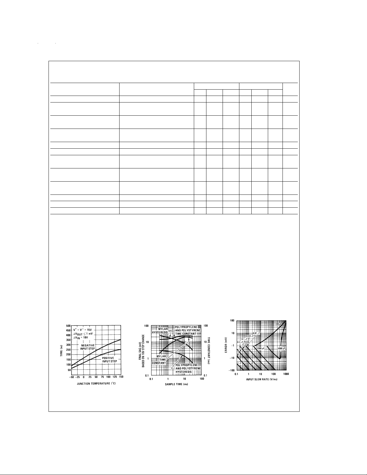
Electrical Characteristics
The following specifcations apply for −VS+ 3.5V ≤ VIN≤ +VS− 3.5V, +V
=
R
10 kΩ, LOGIC REFERENCE=0V, LOGIC HIGH=2.5V, LOGIC LOW=0V unless otherwise specified.
L
=
S
+15V, −V
Parameter Conditions LF198A LF398A Units
Min Typ Max Min Typ Max
=
Input Impedance T
Gain Error T
25˚C 10
j
=
j
25˚C, R
=
10k 0.002 0.005 0.004 0.005
L
Full Temperature Range 0.01 0.01
Feedthrough Attenuation Ratio T
=
j
25˚C, C
=
0.01 µF 86 96 86 90 dB
h
at 1 kHz
Output Impedance T
=
25˚C, “HOLD” mode 0.5 1 0.5 1 Ω
j
Full Temperature Range 4 6 Ω
“HOLD” Step, (Note 6) T
Supply Current, (Note 5) T
Logic and Logic Reference Input T
=
25˚C, C
j
≥25˚C 4.5 5.5 4.5 6.5 mA
j
=
25˚C 2 10 2 10 µA
j
=
h
0.01µF, V
=
0 0.5 1 1.0 1 mV
OUT
Current
Leakage Current into Hold T
=
25˚C, (Note 7) 30 100 30 100 pA
j
Capacitor (Note 5) Hold Mode
Acquisition Time to 0.1
%
Hold Capacitor Charging Current V
Supply Voltage Rejection Ratio V
Differential Logic Threshold T
Note 1: “Absolute Maximum Ratings” indicate limits beyond which damage to the device may occur. Operating Ratings indicate conditions for which the device is
functional, but do not guarantee specific performance limits.
Note 2: The maximum power dissipation must be derated at elevated temperatures and is dictated by T
allowable power dissipation at any temperature is P
junction temperature, T
Note 3: Although the differential voltage may not exceed the limits given, the common-mode voltage on the logic pins may be equal to the supply voltages without
causing damage to the circuit. For proper logic operation, however, one of the logic pins must always be at least 2V below the positive supply and 3V above the negative supply.
Note 4: See AN-450 “Surface Mounting Methods and their effects on Product Reliability” for other methods of soldering surface mount devices.
Note 5: These parameters guaranteed over a supply voltage range of
Note 6: Hold step is sensitive to stray capacitive coupling between input logic signals and the hold capacitor. 1 pF,for instance, will create an additional 0.5 mV step
with a 5V logic swing and a 0.01µF hold capacitor. Magnitude of the hold step is inversely proportional to hold capacitor value.
Note 7: Leakage current is measured at a junction temperature of 25˚C. The effects of junction temperature rise due to power dissipation or elevated ambient can
be calculated by doubling the 25˚C value for each 11˚C increase in chip temperature. Leakage is guaranteed over full input signal range.
Note 8: Amilitary RETS electrical test specification is available on request. The LF198 may also be procured to Standard Military Drawing
MIL-STD-38510 part ID JM38510/12501SGA.
, for the LF198/LF198A is 150˚C; for the LF298, 115˚C; and for the LF398/LF398A, 100˚C.
JMAX
=
∆V
OUT
=
C
0.01 µF 20 25 20 25 µs
h
IN−VOUT
=
0 90 110 90 110 dB
OUT
=
25˚C 0.8 1.4 2.4 0.8 1.4 2.4 V
j
=
(T
D
=
10V, C
=
JMAX−TA
1000 pF 4 6 4 6 µs
h
2V 5 5 mA
)/θJA, or the number given in the Absolute Maximum Ratings, whichever is lower. The maximum
±
5to±18V, and an input range of −VS+ 3.5V ≤ VIN≤ +VS− 3.5V.
=
−15V, T
S
10
, θJA, and the ambient temperature, TA. The maximum
JMAX
=
=
T
25˚C, C
A
j
10
=
h
10
#
5962-8760801GA or to
0.01 µF,
Ω
%
%
Typical Performance Characteristics
Aperture Time
(Note 9)
DS005692-17
Note 9: See Definition of Terms
Dielectric Absorption
Error in Hold Capacitor
DS005692-18
Dynamic Sampling Error
DS005692-19
www.national.com3
Page 4
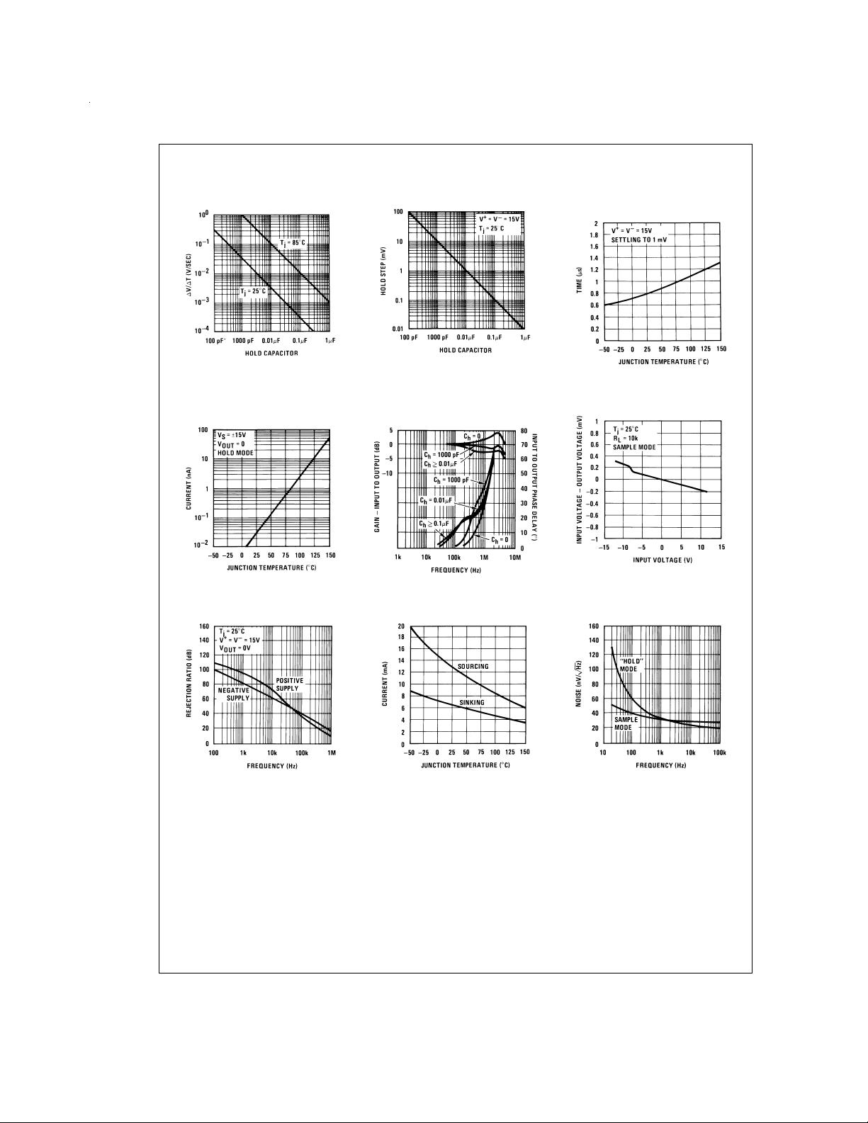
Typical Performance Characteristics (Continued)
Output Droop Rate
Leakage Current into Hold
Capacitor
DS005692-20
DS005692-23
Hold Step
Phase and Gain (Input to
Output, Small Signal)
DS005692-21
DS005692-24
“Hold” Settling Time
(Note 10)
DS005692-22
Gain Error
DS005692-25
Power Supply Rejection
DS005692-26
Note 10: See Definition
Output Short Circuit Current
www.national.com 4
DS005692-27
Output Noise
DS005692-28
Page 5
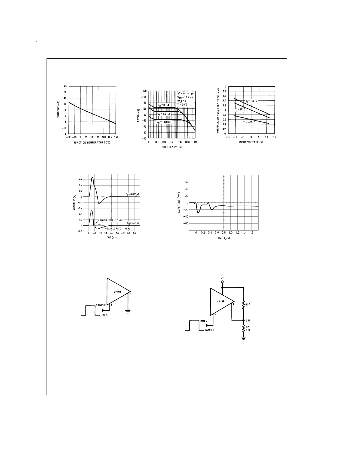
Typical Performance Characteristics (Continued)
Input Bias Current
Output Transient at Start
of Sample Mode
DS005692-29
Feedthrough Rejection Ratio
(Hold Mode)
Output Transient at Start
of Hold Mode
DS005692-12
Hold Step vs Input Voltage
DS005692-31
DS005692-30
DS005692-13
Logic Input Configurations
DS005692-33
Threshold=1.4V
3V ≤ V
TTL & CMOS
(Hi State) ≤ 7V
LOGIC
Threshold=1.4V
*
Select for 2.8V at pin 8
DS005692-34
www.national.com5
Page 6
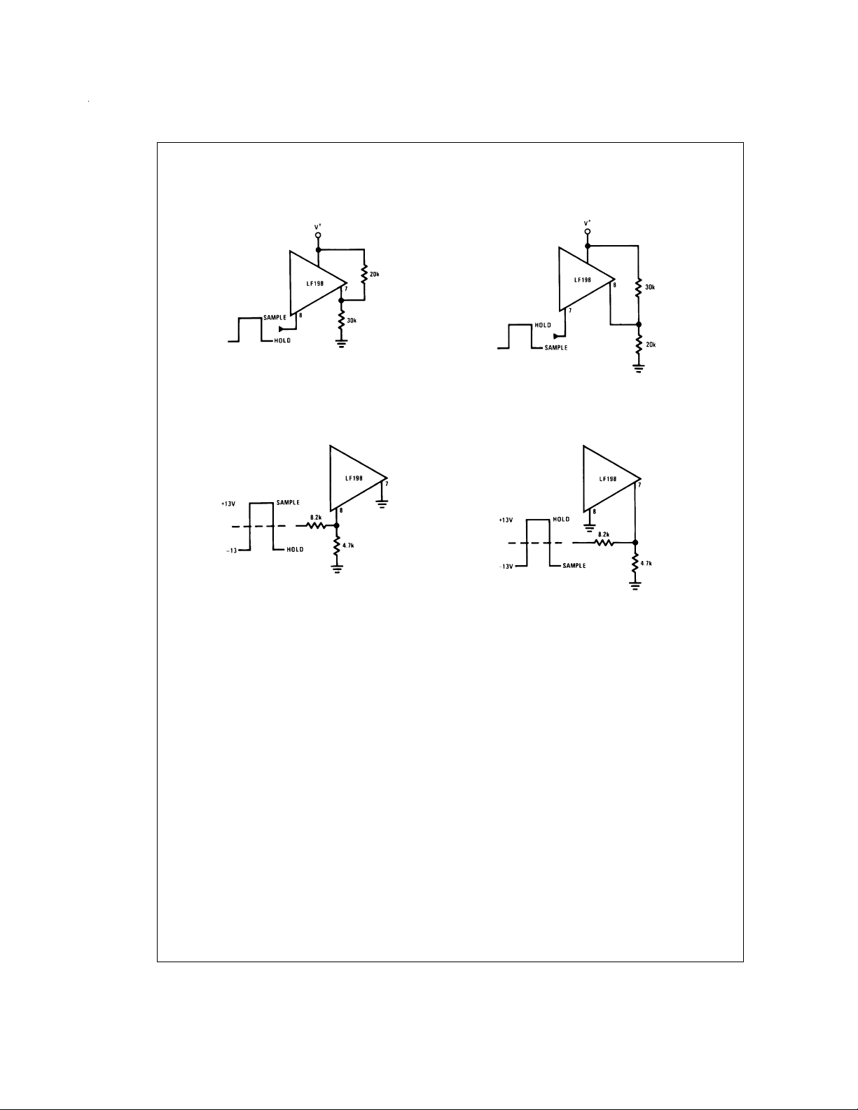
Logic Input Configurations (Continued)
7V ≤ V
LOGIC
Threshold=0.6 (V+) + 1.4V
DS005692-35
Op Amp Drive
Threshold ≈ +4V
DS005692-37
Application Hints
Hold Capacitor
Hold step, acquisition time, and droop rate are the major
trade-offs in the selection of a hold capacitor value. Size and
cost may also become important for larger values. Use of the
curves included with this data sheet should be helpful in selecting a reasonable value of capacitance. Keep in mind that
for fast repetition rates or tracking fast signals, the capacitor
drive currents may cause a significant temperature rise in
the LF198.
A significant source of error in an accurate sample and hold
circuit is dielectric absorption in the hold capacitor. A mylar
cap, for instance, may “sag back” up to 0.2%after a quick
change in voltage. A long sample time is required before the
circuit can be put back into the hold mode with this type of
capacitor. Dielectrics with very low hysteresis are polystyrene, polypropylene, and Teflon. Other types such as mica
and polycarbonate are not nearly as good. The advantage of
polypropylene over polystyrene is that it extends the maximum ambient temperature from 85˚C to 100˚C. Most ceramic capacitors are unusable with
ramic “NPO” or “COG” capacitors are now available for
125˚C operation and also have low dielectric absorption. For
more exact data, see the curve
The hysteresis numbers on the curve are final values, taken
after full relaxation. The hysteresis error can be significantly
>
1%hysteresis. Ce-
Dielectric Absorption Error.
CMOS
(Hi State) ≤ 15V
Threshold=0.6 (V+) − 1.4V
Threshold=−4V
DS005692-36
DS005692-38
reduced if the output of the LF198 is digitized quickly after
the hold mode is initiated. The hysteresis relaxation time
constant in polypropylene, for instance, is 10 — 50 ms. If
A-to-D conversion can be made within 1 ms, hysteresis error
will be reduced by a factor of ten.
DC and AC Zeroing
DC zeroing is accomplished by connecting the offset adjust
pin to the wiper ofa1kΩpotentiometer which has one end
+
tied to V
and the other end tied through a resistor to ground.
The resistor should be selected to give ≈0.6 mA through the
1k potentiometer.
AC zeroing (hold step zeroing) can be obtained by adding an
inverter with the adjustment pot tied input to output. A 10 pF
capacitor from the wiper to the hold capacitor will give
hold step adjustment with a 0.01 µF hold capacitor and 5V
logic supply. For larger logic swings, a smaller capacitor
<
(
10 pF) may be used.
Logic Rise Time
For proper operation, logic signals into the LF198 must have
a minimum dV/dt of 1.0 V/µs. Slower signals will cause excessive hold step. If a R/C network is used in front of the
±
4mV
www.national.com 6
Page 7
Application Hints (Continued)
logic input for signal delay, calculate the slope of the waveform at the threshold point to ensure that it is at least
1.0 V/µs.
Sampling Dynamic Signals
Sample error to moving input signals probably causes more
confusion among sample-and-hold users than any other parameter.The primary reason for this is that many users make
the assumption that the sample and hold amplifier is truly
locked on to the input signal while in the sample mode. In actuality,there are finite phase delays through the circuit creating an input-output differential for fast moving signals. In addition, although the output may have settled, the hold
capacitor has an additional lag due to the 300Ω series resistor on the chip. This means that at the moment the “hold”
command arrives, the hold capacitor voltage may be somewhat different than the actual analog input. The effect of
these delays is opposite to the effect created by delays in the
logic which switches the circuit from sample to hold. For example, consider an analog input of 20 Vp-p at 10 kHz. Maximum dV/dt is 0.6 V/µs. With no analog phase delay and 100
ns logic delay, one could expect up to (0.1 µs) (0.6V/µs)
=
60 mVerror if the “hold” signal arrived near maximum dV/dt
of the input. A positive-going input would give a +60 mV error. Now assume a 1 MHz (3 dB) bandwidth for the overall
analog loop. This generates a phase delay of 160 ns. If the
hold capacitor sees this exact delay, then error due to analog
delay will be (0.16 µs) (0.6 V/µs)=−96 mV. Totaloutput error
is +60 mV (digital) −96 mV (analog) for a total of −36 mV.To
add to the confusion, analog delay is proportioned to hold
capacitor value while digital delay remains constant. A family
of curves (dynamic sampling error) is included to help estimate errors.
A curve labeled
Aperture Time
has been included for sampling conditions where the input is steady during the sampling period, but may experience a sudden change nearly
coincident with the “hold” command. This curve is based on
a 1 mV error fed into the output.
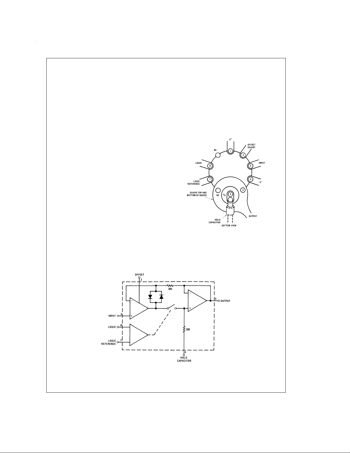
Functional Diagram
A second curve,
Hold Settling Time
indicates the time required for the output to settle to 1 mV after the “hold” command.
Digital Feedthrough
Fast rise time logic signals can cause hold errors by feeding
externally into the analog input at the same time the amplifier
is put into the hold mode. To minimize this problem, board
layout should keep logic lines as far as possible from the
analog input and the C
also be used around the input line, especially if it is driven
pin. Grounded guarding traces may
h
from a high impedance source. Reducing high amplitude
logic signals to 2.5V will also help.
Guarding Technique
DS005692-5
Use 10-pin layout. Guard around Chis tied to output.
DS005692-1
www.national.com7
Page 8
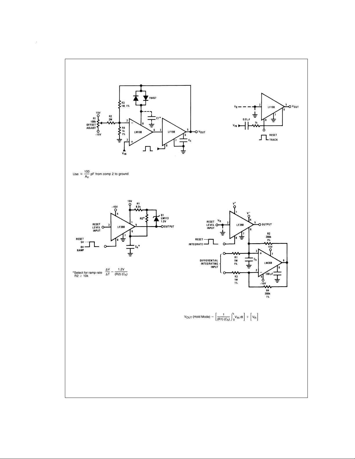
Typical Applications
X1000 Sample & Hold
*
For lower gains, the LM108 must be frequency compensated
Ramp Generator with Variable Reset Level
Sample and Difference Circuit
(Output Follows Input in
Mode)
=
V
+ ∆VIN(HOLD MODE)
V
OUT
B
DS005692-39
Integrator with Programmable Reset Level
Hold
DS005692-40
DS005692-42
www.national.com 8
DS005692-43
Page 9
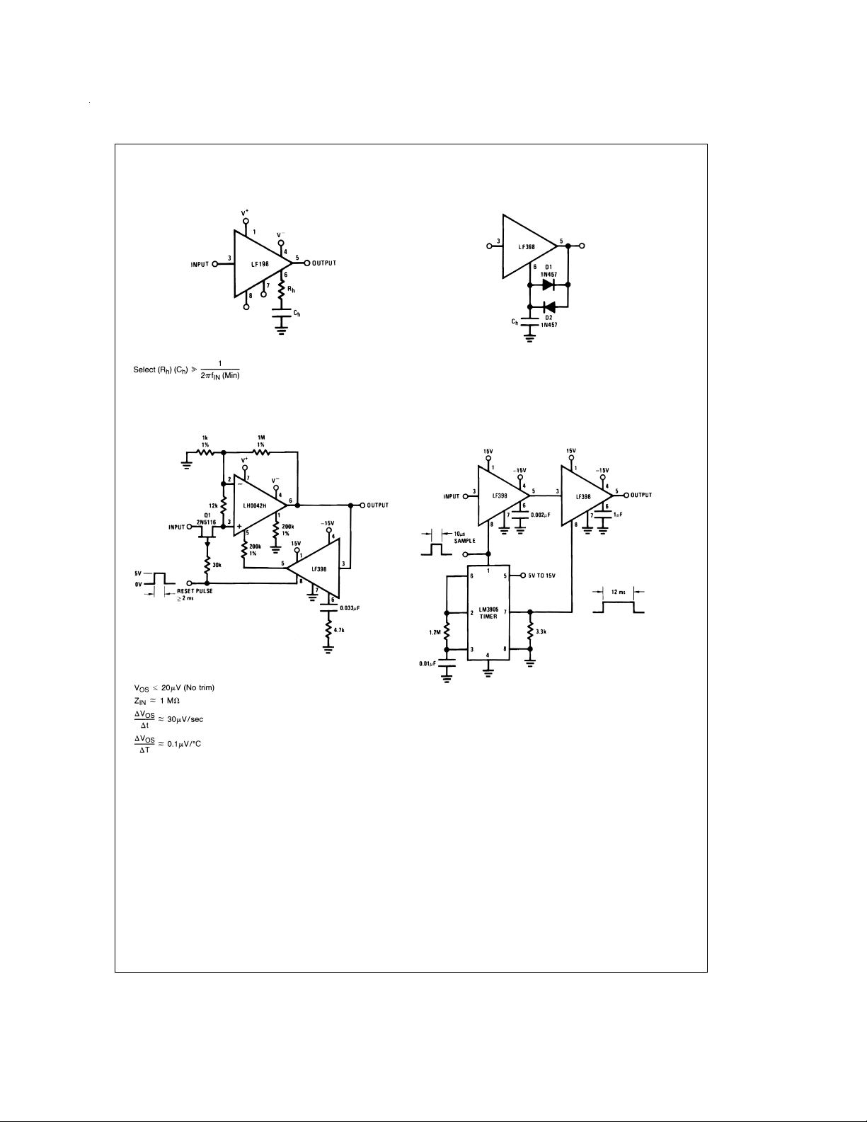
Typical Applications (Continued)
Output Holds at Average of Sampled Input
DS005692-46
Reset Stabilized Amplifier (Gain of 1000)
Increased Slew Current
DS005692-47
Fast Acquisition, Low Droop Sample & Hold
DS005692-49
DS005692-50
www.national.com9
Page 10
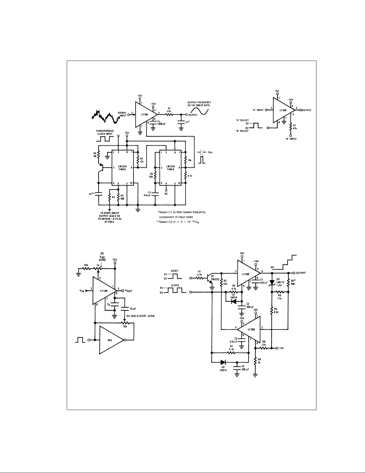
Typical Applications (Continued)
Synchronous Correlator for Recovering
DC & AC Zeroing
Signals Below Noise Level
DS005692-52
Staircase Generator
2–Channel Switch
DS005692-53
AB
Gain 1
Z
IN
BW
±
0.02%1±0.2
1010Ω 47 kΩ
≅
1 MHz
≅
400 kHz
Crosstalk −90 dB −90 dB
@
1 kHz
Offset ≤ 6mV ≤75 mV
%
DS005692-59
*
Select for step height
50k→1V Step
www.national.com 10
DS005692-55
Page 11
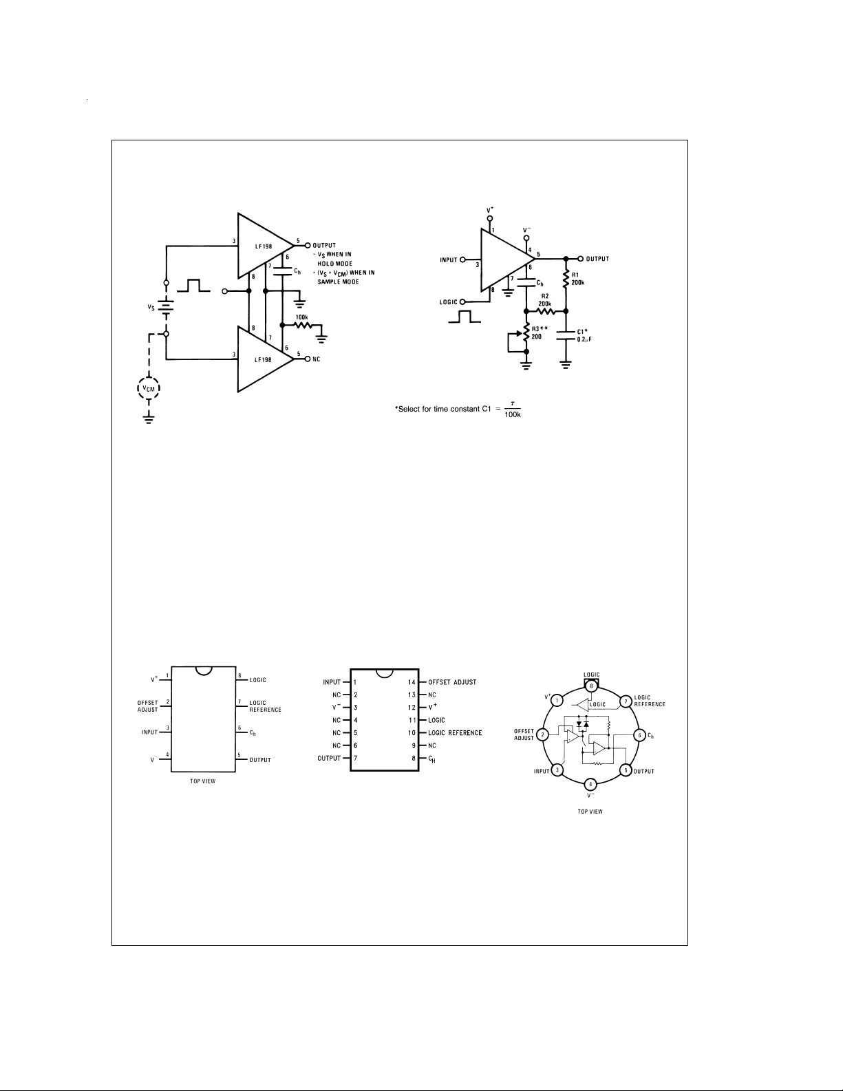
Typical Applications (Continued)
Differential Hold
DS005692-57
Definition of Terms
Hold Step: The voltage step at the output of the sample and
hold when switching from sample mode to hold mode with a
steady (dc) analog input voltage. Logic swing is 5V.
Acquisition Time: The time required to acquire a new analog input voltage with an output step of 10V.Note that acquisition time is not just the time required for the output to settle,
but also includes the time required for all internal nodes to
settle so that the output assumes the proper value when
switched to the hold mode.
Gain Error: The ratio of output voltage swing to input voltage swing in the sample mode expressed as a per cent difference.
Connection Diagrams
Capacitor Hysteresis Compensation
DS005692-56
**
Adjust for amplitude
Hold Settling Time: The time required for the output to
settle within 1 mV of final value after the “hold” logic command.
Dynamic Sampling Error: The error introduced into the
held output due to a changing analog input at the time the
hold command is given. Error is expressed in mV with a
given hold capacitor value and input slew rate. Note that this
error term occurs even for long sample times.
Aperture Time: The delay required between “Hold” command and an input analog transition, so that the transition
does not affect the held output.
Dual-In-Line Package
DS005692-11
Order Number LF398N
or LF398AN
See NS Package Number N08E
Small-Outline Package
DS005692-15
Order Number LF298M or LF398M
See NS Package Number M14A
Metal Can Package
DS005692-14
Order Number LF198H,
LF198H/883, LF298H,
LF398H, LF198AH or LF398AH
See NS Package Number H08C
www.national.com11
Page 12

12
Page 13
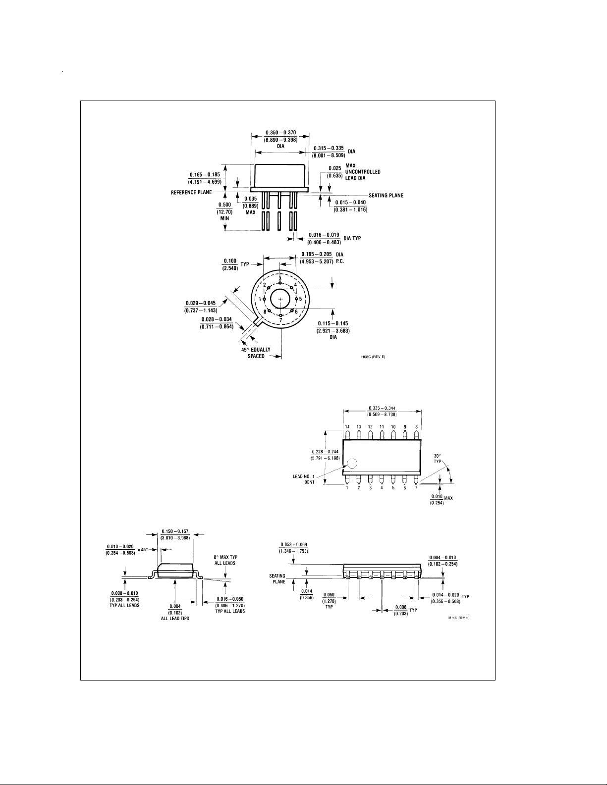
Physical Dimensions inches (millimeters) unless otherwise noted
Order Number LF198H, LF298H, LF398H, LF198AH or LF398AH
Metal Can Package (H)
NS Package Number H08C
Molded Small-Outline Package (M)
Order Number LF298M or LF398M
NS Package Number M14A
www.national.com13
Page 14
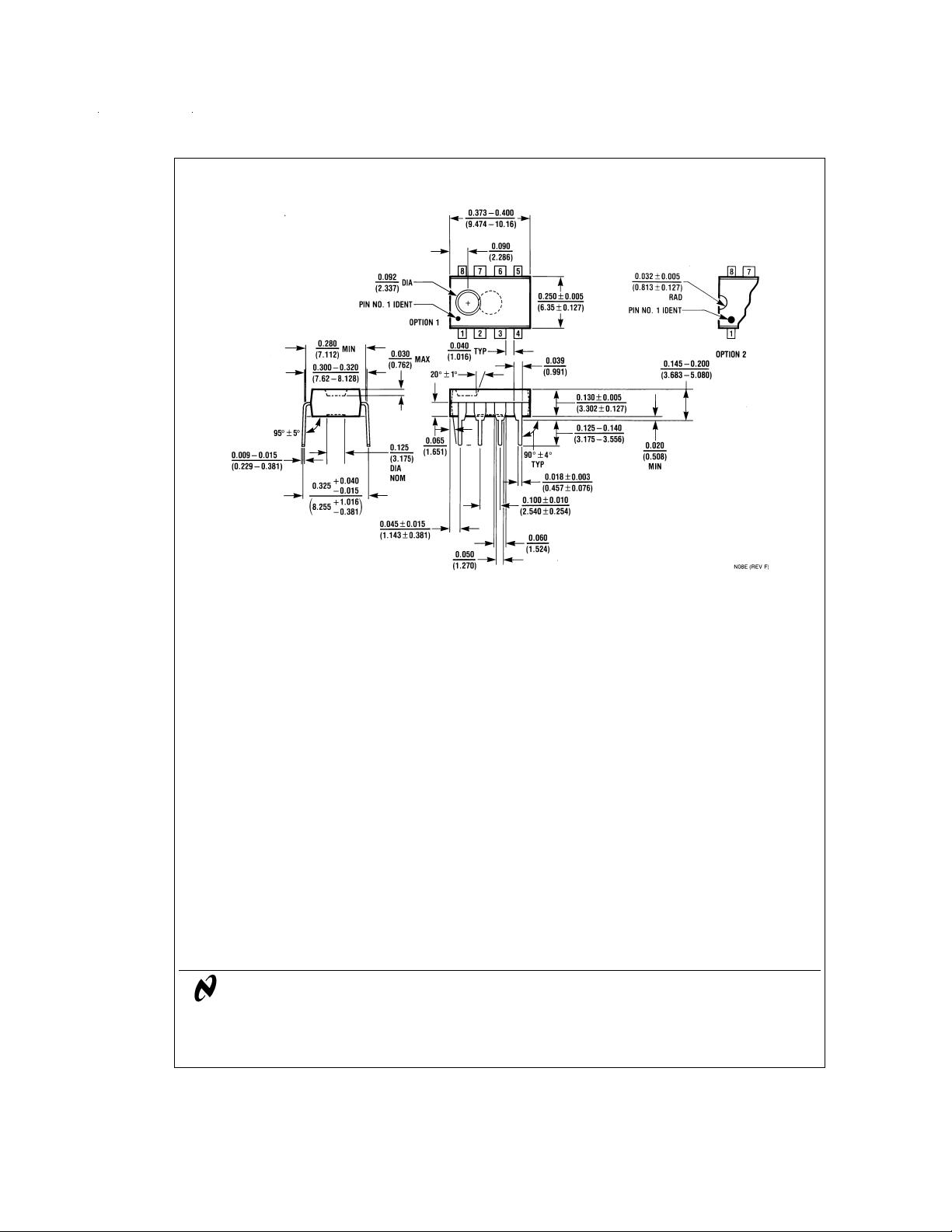
Physical Dimensions inches (millimeters) unless otherwise noted (Continued)
Molded Dual-In-Line Package (N)
Order Number LF398N or LF398AN
NS Package Number N08E
LIFE SUPPORT POLICY
LF198/LF298/LF398, LF198A/LF398A Monolithic Sample-and-Hold Circuits
NATIONAL’S PRODUCTS ARE NOT AUTHORIZED FOR USE AS CRITICAL COMPONENTS IN LIFE SUPPORT DEVICES OR SYSTEMS WITHOUT THE EXPRESS WRITTEN APPROVAL OF THE PRESIDENT OF NATIONAL SEMICONDUCTOR CORPORATION. As used herein:
1. Life support devices or systems are devices or systems which, (a) are intended for surgical implant into
the body, or (b) support or sustain life, and whose failure to perform when properly used in accordance
2. A critical component is any component of a life support
device or system whose failure to perform can be reasonably expected to cause the failure of the life support
device or system, or to affect its safety or effectiveness.
with instructions for use provided in the labeling, can
be reasonably expected to result in a significant injury
to the user.
National Semiconductor
Corporation
Americas
Tel: 1-800-272-9959
Fax: 1-800-737-7018
Email: [email protected]
www.national.com
National does not assume any responsibility for use of any circuitry described, no circuit patent licenses are implied and National reserves the right at any time without notice to change said circuitry and specifications.
National Semiconductor
Europe
Fax: +49 (0) 1 80-530 85 86
Email: [email protected]
Deutsch Tel: +49 (0) 1 80-530 85 85
English Tel: +49 (0) 1 80-532 78 32
Français Tel: +49 (0) 1 80-532 93 58
Italiano Tel: +49 (0) 1 80-534 16 80
National Semiconductor
Asia Pacific Customer
Response Group
Tel: 65-2544466
Fax: 65-2504466
Email: [email protected]
National Semiconductor
Japan Ltd.
Tel: 81-3-5639-7560
Fax: 81-3-5639-7507
 Loading...