

Page 1

查询LF155H供应商
LF155/LF156/LF256/LF257/LF355/LF356/LF357
JFET Input Operational Amplifiers
General Description
These are the first monolithic JFET input operational amplifiers to incorporate well matched, high voltage JFETs on the
same chip with standard bipolar transistors (BI-FET
nology). These amplifiers feature low input bias and offset
currents/low offset voltage and offset voltage drift, coupled
with offset adjust which does not degrade drift or
common-mode rejection. The devices are also designed for
high slew rate, wide bandwidth, extremely fast settling time,
low voltage and current noise and a low 1/f noise corner.
™
Tech-
Features
Advantages
n Replace expensive hybrid and module FET op amps
n Rugged JFETs allow blow-out free handling compared
with MOSFET input devices
n Excellent for low noise applications using either high or
low source impedance—very low 1/f corner
n Offset adjust does not degrade drift or common-mode
rejection as in most monolithic amplifiers
n New output stage allows use of large capacitive loads
(5,000 pF) without stability problems
n Internal compensation and large differential input voltage
capability
Applications
n Precision high speed integrators
n Fast D/A and A/D converters
n High impedance buffers
n Wideband, low noise, low drift amplifiers
n Logarithmic amplifiers
n Photocell amplifiers
n Sample and Hold circuits
Common Features
n Low input bias current: 30pA
n Low Input Offset Current: 3pA
n High input impedance: 10
n Low input noise current:
n High common-mode rejection ratio: 100 dB
n Large dc voltage gain: 106 dB
Uncommon Features
LF155/
LF355
j
Extremely
fast settling
time to
0.01%
j
Fast slew
rate
j
Wide gain
bandwidth
j
Low input
noise
voltage
December 2001
12
Ω
LF156/
LF256/
LF356
4 1.5 1.5 µs
5 12 50 V/µs
2.5 5 20 MHz
20 12 12
LF257/
LF357
(A
V
Units
=5)
LF155/LF156/LF256/LF257/LF355/LF356/LF357 JFET Input Operational Amplifiers
Simplified Schematic
*
3pF in LF357 series.
BI-FET™, BI-FET II™are trademarks of National Semiconductor Corporation.
© 2001 National Semiconductor Corporation DS005646 www.national.com
00564601
Page 2

Absolute Maximum Ratings (Note 1)
If Military/Aerospace specified devices are required, contact the National Semiconductor Sales Office/Distributors for
availability and specifications.
LF155/6 LF256/7/LF356B LF355/6/7
Supply Voltage
Differential Input Voltage
Input Voltage Range (Note 2)
Output Short Circuit Duration Continuous Continuous Continuous
T
JMAX
H-Package 150˚C 115˚C 115˚C
N-Package 100˚C 100˚C
M-Package 100˚C 100˚C
Power Dissipation at T
= 25˚C (Notes
A
1, 8)
H-Package (Still Air) 560 mW 400 mW 400 mW
LF155/LF156/LF256/LF257/LF355/LF356/LF357
H-Package (400 LF/Min Air Flow) 1200 mW 1000 mW 1000 mW
N-Package 670 mW 670 mW
M-Package 380 mW 380 mW
Thermal Resistance (Typical) θ
JA
H-Package (Still Air) 160˚C/W 160˚C/W 160˚C/W
H-Package (400 LF/Min Air Flow) 65˚C/W 65˚C/W 65˚C/W
N-Package 130˚C/W 130˚C/W
M-Package 195˚C/W 195˚C/W
(Typical) θ
JC
H-Package 23˚C/W 23˚C/W 23˚C/W
Storage Temperature Range −65˚C to +150˚C −65˚C to +150˚C −65˚C to +150˚C
Soldering Information (Lead Temp.)
Metal Can Package
Soldering (10 sec.) 300˚C 300˚C 300˚C
Dual-In-Line Package
Soldering (10 sec.) 260˚C 260˚C 260˚C
Small Outline Package
Vapor Phase (60 sec.) 215˚C 215˚C
Infrared (15 sec.) 220˚C 220˚C
See AN-450 “Surface Mounting Methods and Their Effect on Product Reliability” for other methods of
soldering surface mount devices.
ESD tolerance
(100 pF discharged through 1.5kΩ) 1000V 1000V 1000V
±
±
±
22V
40V
20V
±
±
±
22V
40V
20V
±
±
±
18V
30V
16V
DC Electrical Characteristics
(Note 3)
Symbol Parameter Conditions
Min Typ Max Min Typ Max Min Typ Max
V
OS
∆V
OS
∆TC/∆V
I
OS
www.national.com 2
Input Offset Voltage RS=50Ω,TA=25˚C 3 5 3 5 3 10 mV
Over Temperature 7 6.5 13 mV
/∆T Average TC of Input
RS=50Ω
Offset Voltage
Change in Average TC
OS
OS
Adjust
with V
R
=50Ω, (Note 4)
S
Input Offset Current TJ=25˚C, (Notes 3, 5) 3 20 3 20 3 50 pA
T
J≤THIGH
LF155/6
LF256/7
LF356B
LF355/6/7
5 5 5 µV/˚C
0.5 0.5 0.5
20 1 2 nA
Units
µV/˚C
per mV
Page 3

DC Electrical Characteristics (Continued)
(Note 3)
Symbol Parameter Conditions
I
B
R
IN
A
VOL
Input Bias Current TJ=25˚C, (Notes 3, 5) 30 100 30 100 30 200 pA
T
J≤THIGH
Input Resistance TJ=25˚C 10
Large Signal Voltage
Gain
VS=±15V, TA=25˚C 50 200 50 200 25 200 V/mV
V
=±10V, RL=2k
O
Over Temperature 25 25 15 V/mV
V
O
V
CM
Output Voltage Swing VS=±15V, RL=10k
V
=±15V, RL=2k
S
Input Common-Mode
VS=±15V
Voltage Range
CMRR Common-Mode
Rejection Ratio
PSRR Supply Voltage
(Note 6)
Rejection Ratio
DC Electrical Characteristics
TA=TJ= 25˚C, VS=±15V
Parameter
Supply
Current
LF155 LF355 LF156/256/257/356B LF356 LF357
Typ Max Typ Max Typ Max Typ Max Typ Max
2424 5 7 510510mA
LF155/6
LF256/7
LF356B
LF355/6/7
Units
Min Typ Max Min Typ Max Min Typ Max
50 5 8 nA
12
±
12±13
±10±
±
12
+15.1
11
−12 −12 −12 V
±
±
±
10
12±13
10±12
±
15.1
11
12
±
±
+10
12
10
12±13 V
10±12 V
+15.1 V
85 100 85 100 80 100 dB
85 100 85 100 80 100 dB
Units
LF155/LF156/LF256/LF257/LF355/LF356/LF357
Ω
AC Electrical Characteristics
TA=TJ= 25˚C, VS=±15V
Symbol Parameter Conditions
LF155/355 LF156/256/
356B
LF156/256/356/
LF356B
LF257/357
Units
Typ Min Typ Typ
SR Slew Rate LF155/6:
A
=1,
V
LF357: A
=5 50 V/µs
V
5 7.5 12 V/µs
GBW Gain Bandwidth Product 2.5 5 20 MHz
t
s
e
n
Settling Time to 0.01% (Note 7) 4 1.5 1.5 µs
Equivalent Input Noise
Voltage
RS=100Ω
f=100 Hz 25 15 15
f=1000 Hz 20 12 12
i
n
C
IN
Equivalent Input Current
Noise
f=100 Hz 0.01 0.01 0.01
f=1000 Hz 0.01 0.01 0.01
Input Capacitance 3 3 3 pF
Notes for Electrical Characteristics
Note 1: The maximum power dissipation for these devices must be derated at elevated temperatures and is dictated by T
. The maximum available power dissipation at any temperature is PD=(T
T
A
Note 2: Unless otherwise specified the absolute maximum negative input voltage is equal to the negative power supply voltage.
Note 3: Unless otherwise stated, these test conditions apply:
JMAX−TA
)/θJAor the 25˚C P
, whichever is less.
dMAX
, θJA, and the ambient temperature,
JMAX
www.national.com3
Page 4
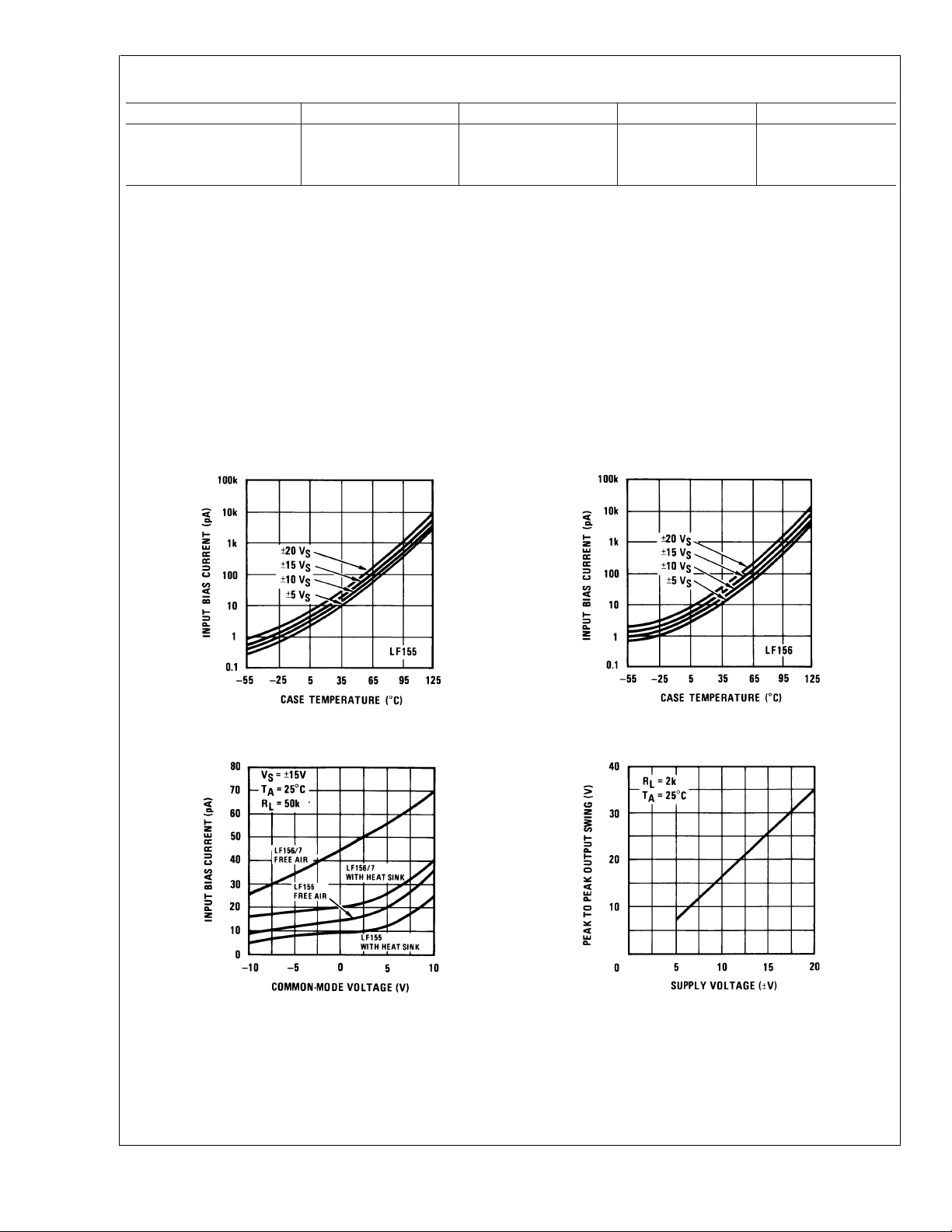
Notes for Electrical Characteristics (Continued)
LF155/156 LF256/257 LF356B LF355/6/7
Supply Voltage, V
T
A
T
HIGH
and VOS,IBand IOSare measured at VCM=0.
Note 4: The Temperature Coefficient of the adjusted input offset voltage changesonly a small amount(0.5µV/˚C typically) for each mV of adjustment from its original
unadjusted value. Common-mode rejection and open loop voltage gain are also unaffected by offset adjustment.
Note 5: The input bias currents are junction leakage currents which approximately double for every 10˚C increase in the junction temperature, T
production test time, the input bias currents measured are correlated to junction temperature. In normal operation the junction temperature rises above the ambient
temperature as a result of internal power dissipation, Pd. T
recommended if input bias current is to be kept to a minimum.
Note 6: Supply Voltage Rejection is measured for both supply magnitudes increasing or decreasing simultaneously, in accordance with common practice.
Note 7: Settling time is definedhere, for a unity gain inverter connection using2 kΩ resistors for the LF155/6. It is the time required for the error voltage (the voltage
at the inverting input pin on the amplifier) to settle to within 0.01% of its final value from the time a 10V step input is applied to the inverter. For the LF357, A
the feedback resistor from output to input is 2kΩ and the output step is 10V (See Settling Time Test Circuit).
Note 8: Max. PowerDissipation is defined bythe package characteristics. Operatingthe part near theMax. Power Dissipation may cause the part to operate outside
guaranteed limits.
S
±
15V ≤ VS≤±20V
−55˚C ≤ TA≤ +125˚C −25˚C ≤ TA≤ +85˚C 0˚C ≤ TA≤ +70˚C 0˚C ≤ TA≤ +70˚C
+125˚C +85˚C +70˚C +70˚C
J=TA+θJA
±
15V ≤ VS≤±20V
Pd where θJAis the thermal resistance from junction to ambient. Use of a heat sink is
±
15V ≤ V
±
20V VS=±15V
S
LF155/LF156/LF256/LF257/LF355/LF356/LF357
Typical DC Performance Characteristics Curves are for LF155 and LF156 unless otherwise
specified.
Input Bias Current Input Bias Current
. Due to limited
J
= −5,
V
00564637
Input Bias Current Voltage Swing
00564639
www.national.com 4
00564638
00564640
Page 5

Typical DC Performance Characteristics Curves are for LF155 and LF156 unless otherwise
specified. (Continued)
Supply Current Supply Current
LF155/LF156/LF256/LF257/LF355/LF356/LF357
00564641
Negative Current Limit Positive Current Limit
00564643
Positive Common-Mode
Input Voltage Limit
Negative Common-Mode
Input Voltage Limit
00564642
00564644
00564645
00564646
www.national.com5
Page 6
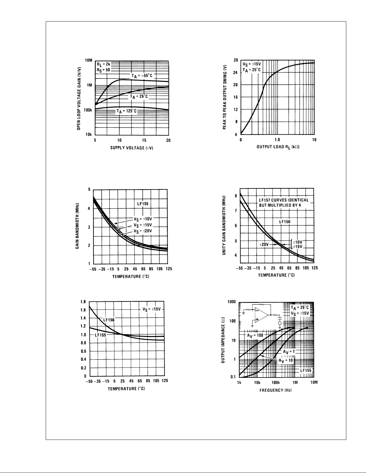
Typical DC Performance Characteristics Curves are for LF155 and LF156 unless otherwise
specified. (Continued)
Open Loop Voltage Gain Output Voltage Swing
LF155/LF156/LF256/LF257/LF355/LF356/LF357
00564647
Typical AC Performance Characteristics
Gain Bandwidth Gain Bandwidth
00564649
Normalized Slew Rate Output Impedance
00564648
00564650
00564651
www.national.com 6
00564652
Page 7

Typical AC Performance Characteristics (Continued)
LF155/LF156/LF256/LF257/LF355/LF356/LF357
Output Impedance LF155 Small Signal Pulse Response, A
00564653
00564605
V
=+1
LF156 Small Signal Pulse Response, AV= +1 LF155 Large Signal Pulse Response, AV=+1
LF156 Large Signal Puls
Response, A
= +1 Inverter Settling Time
V
00564606
00564609
00564608
00564655
www.national.com7
Page 8
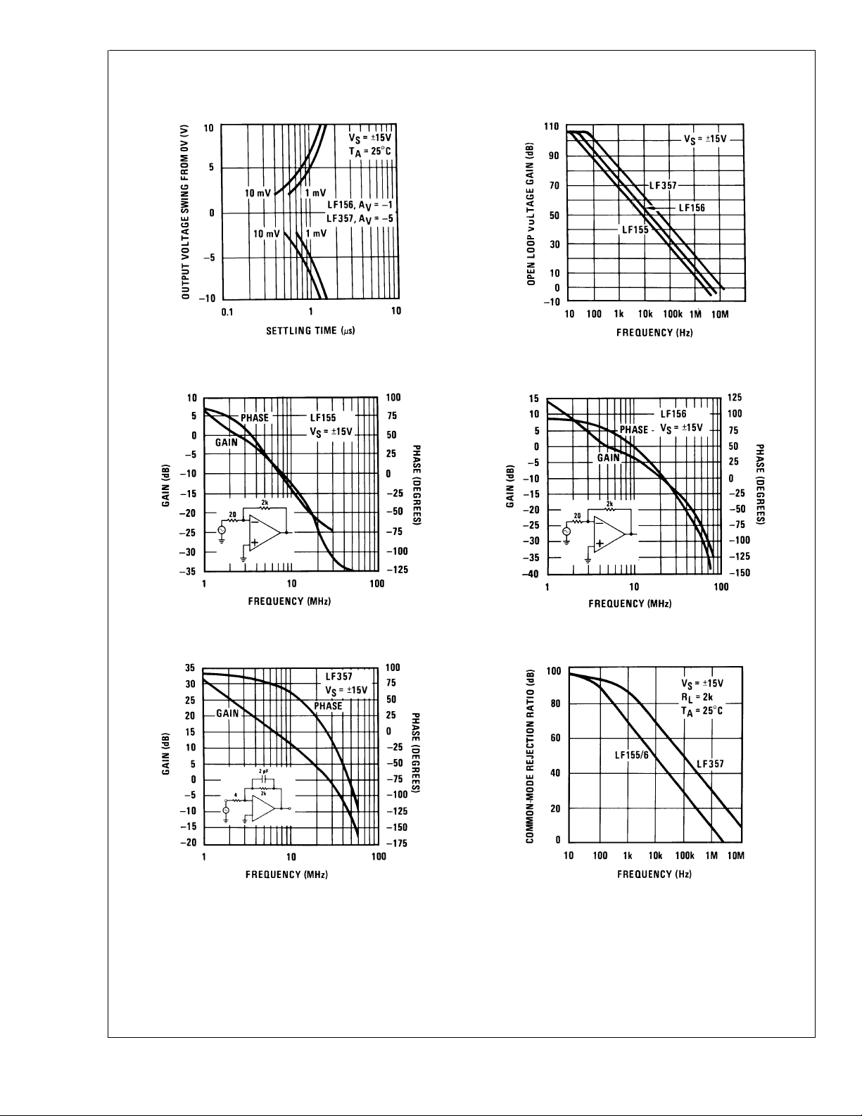
Typical AC Performance Characteristics (Continued)
Inverter Settling Time Open Loop Frequency Response
LF155/LF156/LF256/LF257/LF355/LF356/LF357
00564656
Bode Plot Bode Plot
00564658
Bode Plot Common-Mode Rejection Ratio
00564657
00564659
00564660
www.national.com 8
00564661
Page 9
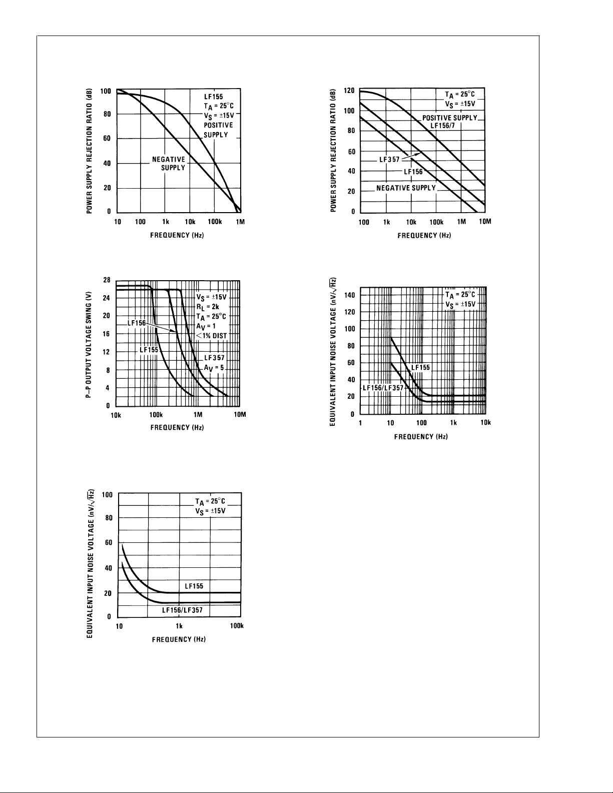
Typical AC Performance Characteristics (Continued)
Power Supply Rejection Ratio Power Supply Rejection Ratio
LF155/LF156/LF256/LF257/LF355/LF356/LF357
00564662
Undistorted Output Voltage Swing Equivalent Input Noise Voltage
00564664
Equivalent Input Noise
Voltage (Expanded Scale)
00564663
00564665
00564666
www.national.com9
Page 10
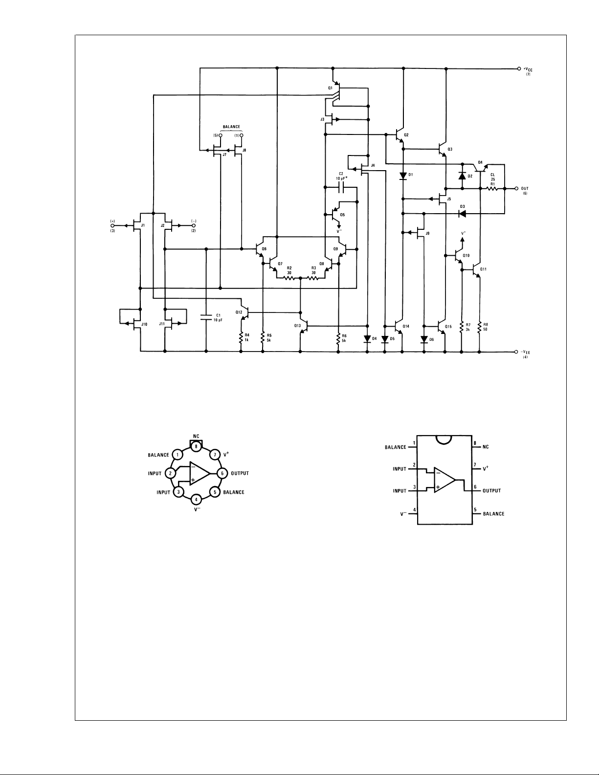
Detailed Schematic
LF155/LF156/LF256/LF257/LF355/LF356/LF357
*
C = 3pF in LF357 series.
Connection Diagrams (Top Views)
Metal Can Package (H)
Order Number LF155H, LF156H, LF256H, LF257H,
LF356BH, LF356H, or LF357H
See NS Package Number H08C
*
Available per JM38510/11401 or JM38510/11402
00564614
00564613
Dual-In-Line Package (M and N)
00564629
Order Number LF356M, LF356MX, LF355N, or LF356N
See NS Package Number M08A or N08E
Application Hints
These are op amps with JFET input devices. These JFETs
have large reverse breakdown voltages from gate to source
and drain eliminating the need for clamps across the inputs.
Therefore large differential input voltages can easily be accommodated without a large increase in input current. The
maximum differential input voltage is independent of the
supply voltages. However, neither of the input voltages
should be allowed to exceed the negative supply as this will
cause large currents to flow which can result in a destroyed
unit.
Exceeding the negative common-mode limit on either input
will force the output to a high state, potentially causing a
www.national.com 10
Page 11
LF155/LF156/LF256/LF257/LF355/LF356/LF357
Application Hints (Continued)
reversal of phase to the output. Exceeding the negative
common-mode limit on both inputs will force the amplifier
output to a high state. In neither case does a latch occur
since raising the input back within the common-mode range
again puts the input stage and thus the amplifier in a normal
operating mode.
Exceeding the positive common-mode limit on a single input
will not change the phase of the output however, if both
inputs exceed the limit, the output of the amplifier will be
forced to a high state.
These amplifiers will operate with the common-mode input
voltage equal to the positive supply. In fact, the
common-mode voltage can exceed the positive supply by
approximately 100 mV independent of supply voltage and
over the full operating temperature range. The positive supply can therefore be used as a reference on an input as, for
example, in a supply current monitor and/or limiter.
Precautions should be taken to ensure that the power supply
for the integrated circuit never becomes reversed in polarity
or that the unit is not inadvertently installed backwards in a
socket as an unlimited current surge through the resulting
forward diode within the IC could cause fusing of the internal
conductors and result in a destroyed unit.
All of the bias currents in these amplifiers are set by FET
current sources. The drain currents for the amplifiers are
therefore essentially independent of supply voltage.
As with most amplifiers, care should be taken with lead
dress, component placement and supply decoupling in order
to ensure stability. For example, resistors from the output to
an input should be placed with the body close to the input to
minimize “pickup” and maximize the frequency of the feedback pole by minimizing the capacitance from the input to
ground.
A feedback pole is created when the feedback around any
amplifier is resistive. The parallel resistanceand capacitance
from the input of the device (usually the invertinginput) toAC
ground set the frequency of the pole. In many instances the
frequency of this pole is much greater than the expected 3dB
frequency of the closed loop gain and consequently there is
negligible effect on stability margin. However, if the feedback
pole is less than approximately six times the expected 3 dB
frequency a lead capacitor should be placed from the output
to the input of the op amp. The value of the added capacitor
should be such that the RC time constant of this capacitor
and the resistance it parallels is greater than or equal to the
original feedback pole time constant.
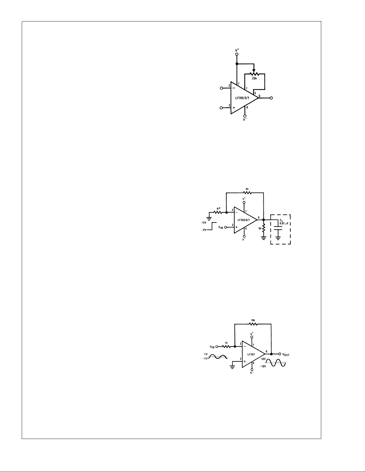
Typical Circuit Connections
VOSAdjustment
00564667
VOSis adjusted with a 25k potentiometer
•
The potentiometer wiper is connected to V
•
For potentiometers with temperature coefficient of 100
•
ppm/˚C or less the additional drift with adjust is ≈ 0.5µV/
˚C/mV of adjustment
Typical overall drift: 5µV/˚C±(0.5µV/˚C/mV of adj.)
•
Driving Capacitive Loads
*
LF155/6 R = 5k
LF357 R = 1.25k
Due to a unique output stage design, these amplifiers
have the ability to drive large capacitive loads and still
maintain stability. C
L(MAX)
. 0.01µF.
Overshoot ≤ 20%
Settling time (t
) . 5µs
s
LF357. A Large Power BW Amplifier
+
00564668
For distortion ≤ 1% and a 20 Vp-p V
500kHz.
swing, power bandwidth is:
OUT
00564615
www.national.com11
Page 12
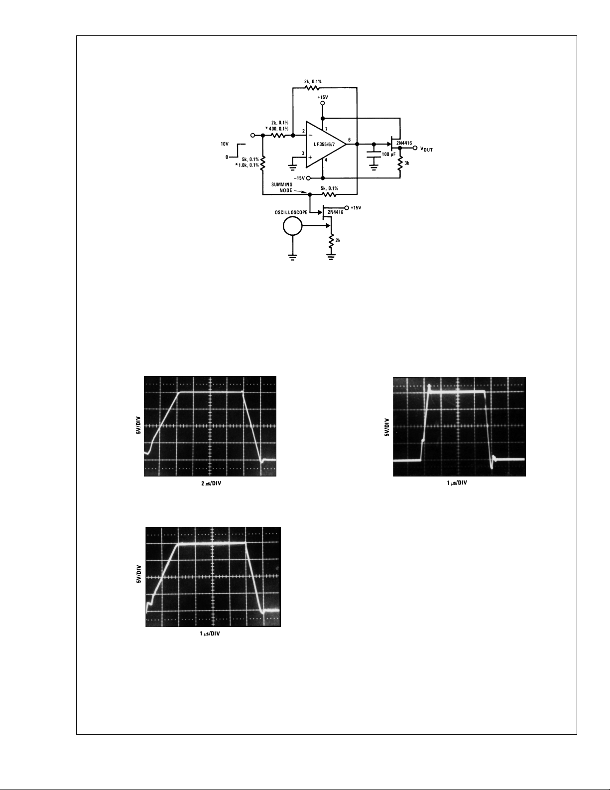
Typical Applications
Settling Time Test Circuit
LF155/LF156/LF256/LF257/LF355/LF356/LF357
Settling time is tested with the LF155/6 connected as unity gain inverter and LF357 connected for AV=−5
•
FET used to isolate the probe capacitance
•
Output = 10V step
•
AV= −5 for LF357
•
00564616
Large Signal Inverter Output, V
LF355
00564617
LF356
(from Settling Time Circuit)
OUT
LF357
00564619
00564618
www.national.com 12
Page 13
Typical Applications (Continued)
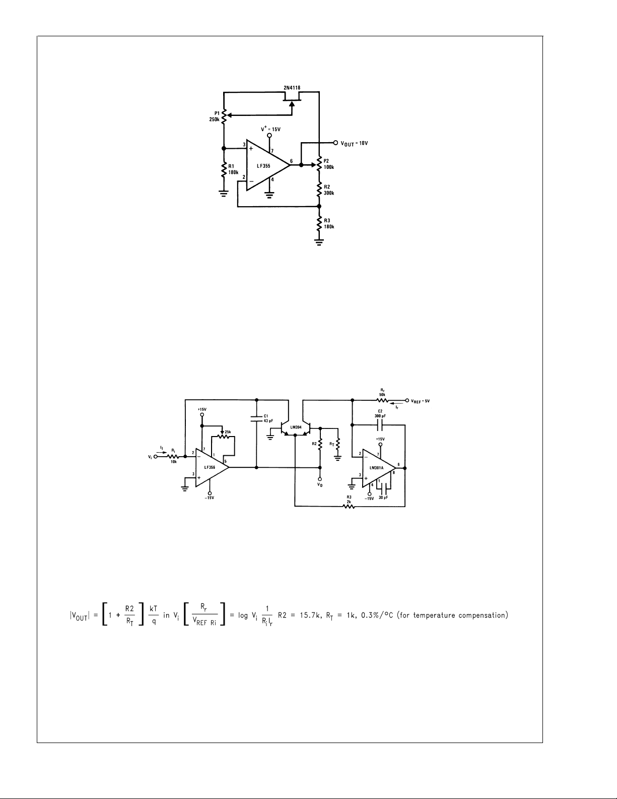
Low Drift Adjustable Voltage Reference
∆ V
•
•
•
•
•
/∆T=±0.002%/˚C
OUT
All resistors and potentiometers should be wire-wound
P1: drift adjust
P2: V
OUT
adjust
Use LF155 for
j
Low I
B
j
Low drift
j
Low supply current
Fast Logarithmic Converter
LF155/LF156/LF256/LF257/LF355/LF356/LF357
00564620
Dynamic range: 100µA ≤ Ii≤ 1mA (5 decades), |VO| = 1V/decade
•
Transient response: 3µs for ∆Ii= 1 decade
•
C1, C2, R2, R3: added dynamic compensation
•
VOSadjust the LF156 to minimize quiescent error
•
RT: Tel Labs type Q81 + 0.3%/˚C
•
00564621
www.national.com13
Page 14
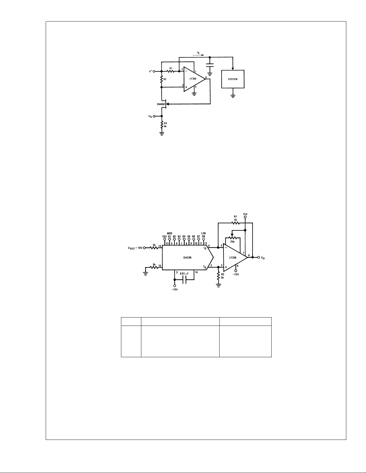
Typical Applications (Continued)
Precision Current Monitor
VO= 5 R1/R2 (V/mA of IS)
•
LF155/LF156/LF256/LF257/LF355/LF356/LF357
R1, R2, R3: 0.1% resistors
•
Use LF155 for
•
j
Common-mode range to supply range
j
Low I
B
j
Low V
OS
j
Low Supply Current
8-Bit D/A Converter with Symmetrical Offset Binary Operation
00564631
R1, R2 should be matched within±0.05%
•
Full-scale response time: 3µs
•
EOB1 B2 B3 B4 B5 B6 B7 B8 Comments
+9.920 11111111 Positive Full-Scale
+0.040 10000000 (+)Zero-Scale
−0.040 01111111 (−)Zero-Scale
−9.920 00000000Negative Full-Scale
www.national.com 14
00564632
Page 15
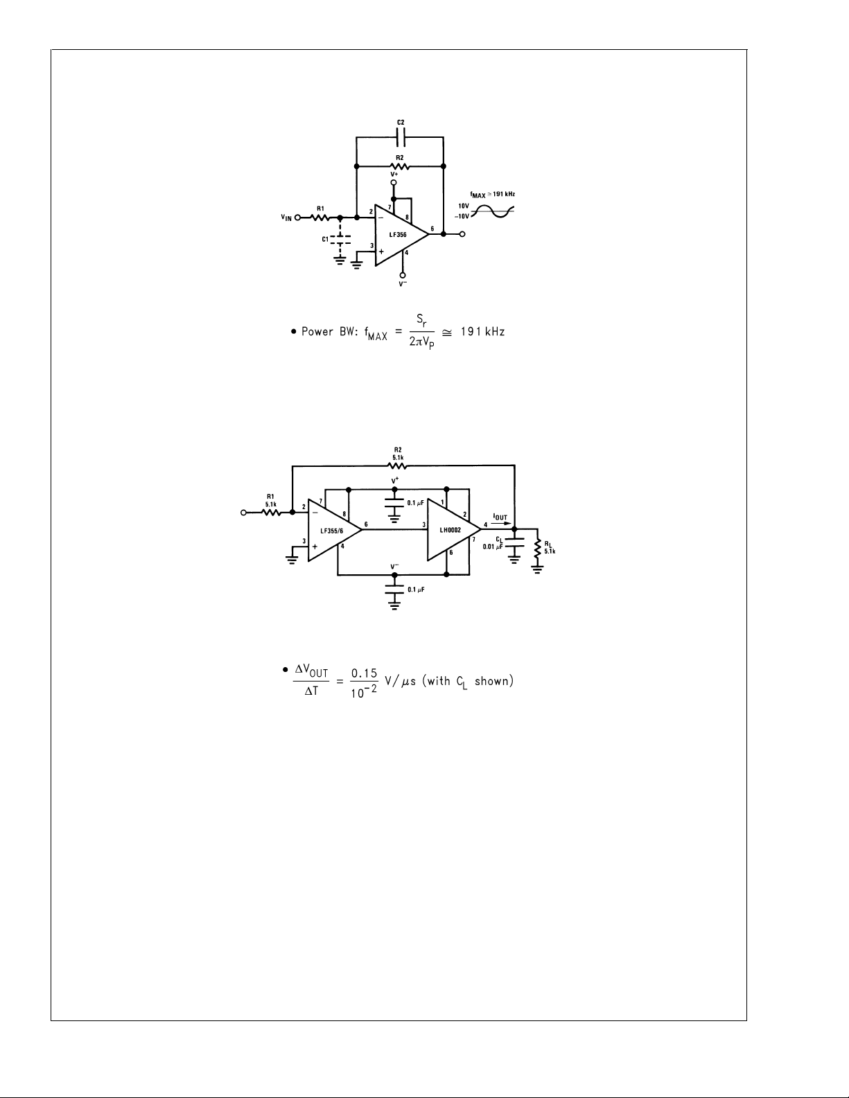
Typical Applications (Continued)
Wide BW Low Noise, Low Drift Amplifier
00564670
Parasitic input capacitance C1 . (3pF for LF155, LF156 and LF357 plus any additional layout capacitance) interacts with
•
feedback elements and creates undesirable high frequency pole. To compensate add C2 such that: R2 C2 . R1 C1.
Boosting the LF156 with a Current Amplifier
LF155/LF156/LF256/LF257/LF355/LF356/LF357
I
•
OUT(MAX)
No additional phase shift added by the current amplifier
•
.150mA (will drive RL≥ 100Ω)
00564673
www.national.com15
Page 16
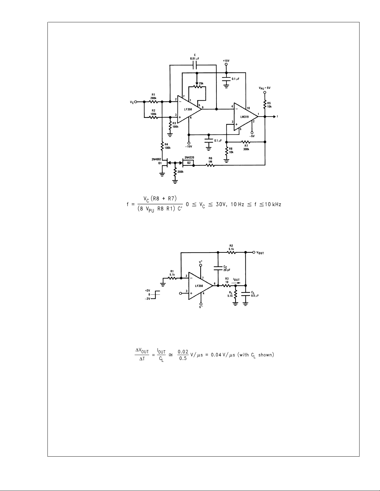
Typical Applications (Continued)
LF155/LF156/LF256/LF257/LF355/LF356/LF357
3 Decades VCO
00564624
R1, R4 matched. Linearity 0.1% over 2 decades.
Overshoot 6%
•
ts10µs
•
When driving large CL, the V
•
OUT
Isolating Large Capacitive Loads
slew rate determined by CLand I
OUT(MAX)
00564622
:
www.national.com 16
Page 17
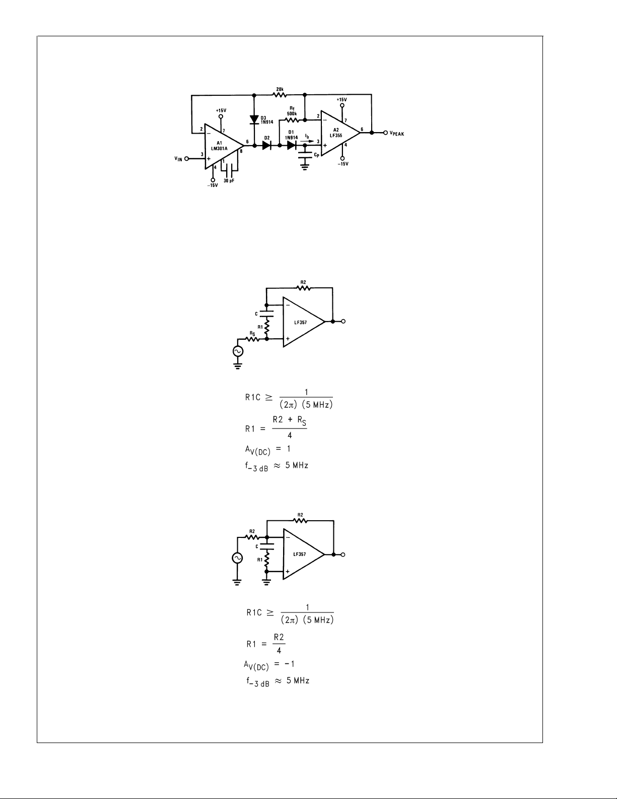
Typical Applications (Continued)
Low Drift Peak Detector
00564623
By adding D1 and Rf,VD1=0 during hold mode. Leakage of D2 provided by feedback path through Rf.
•
Leakage of circuit is essentially Ib(LF155, LF156) plus capacitor leakage of Cp.
•
Diode D3 clamps V
•
Maximum input frequency should be
•
(A1) to VIN−VD3to improve speed and to limit reverse bias of D2.
OUT
1
<<
⁄2πRfCD2where CD2is the shunt capacitance of D2.
Non-Inverting Unity Gain Operation for LF157
LF155/LF156/LF256/LF257/LF355/LF356/LF357
00564675
Inverting Unity Gain for LF157
00564625
www.national.com17
Page 18
Typical Applications (Continued)
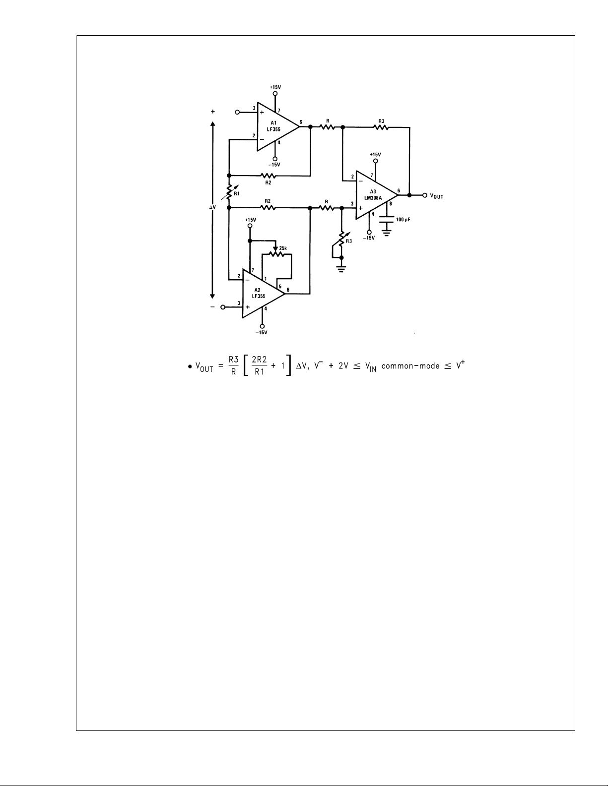
High Impedance, Low Drift Instrumentation Amplifier
LF155/LF156/LF256/LF257/LF355/LF356/LF357
00564626
System VOSadjusted via A2 VOSadjust
•
TrimR3 to boost up CMRR to 120 dB. Instrumentation amplifier resistor array recommended for best accuracy and lowest drift
•
www.national.com 18
Page 19
Typical Applications (Continued)
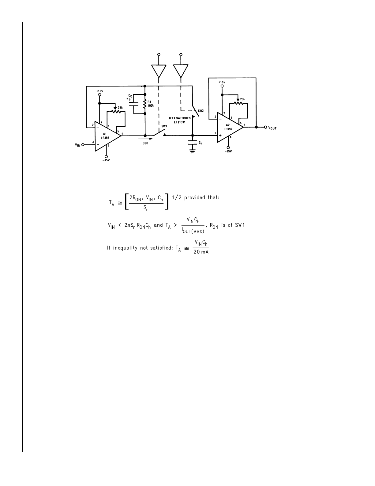
Fast Sample and Hold
00564633
Both amplifiers (A1, A2) have feedback loops individually closed with stable responses (overshoot negligible)
•
Acquisition time TA, estimated by:
•
LF155/LF156/LF256/LF257/LF355/LF356/LF357
LF156 develops full Sroutput capability for VIN≥ 1V
•
Addition of SW2 improves accuracy by putting the voltage drop across SW1 inside the feedback loop
•
Overall accuracy of system determined by the accuracy of both amplifiers, A1 and A2
•
www.national.com19
Page 20
Typical Applications (Continued)
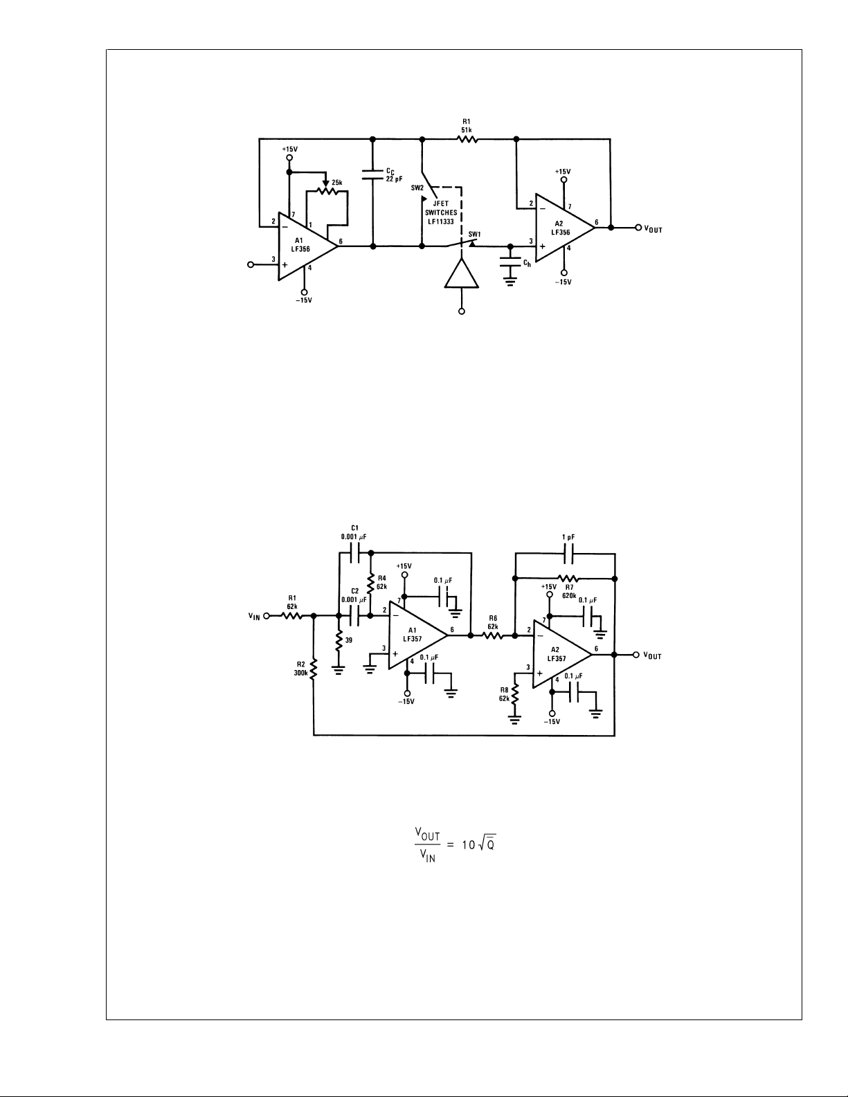
High Accuracy Sample and Hold
LF155/LF156/LF256/LF257/LF355/LF356/LF357
No V
TAcan be estimated by same considerations as previously but, because of the added
•
adjust required for A2.
OS
By closing the loop through A2, the V
•
propagation delay in the feedback loop (A2) the overshoot is not negligible.
Overall system slower than fast sample and hold
•
R1, CC: additional compensation
•
Use LF156 for
•
j
Fast settling time
j
Low V
OS
accuracy will be determined uniquely by A1.
OUT
High Q Band Pass Filter
00564627
By adding positive feedback (R2)
•
Q increases to 40
•
fBP= 100 kHz
•
Clean layout recommended
•
Response to a 1Vp-p tone burst: 300µs
•
www.national.com 20
00564628
Page 21
Typical Applications (Continued)
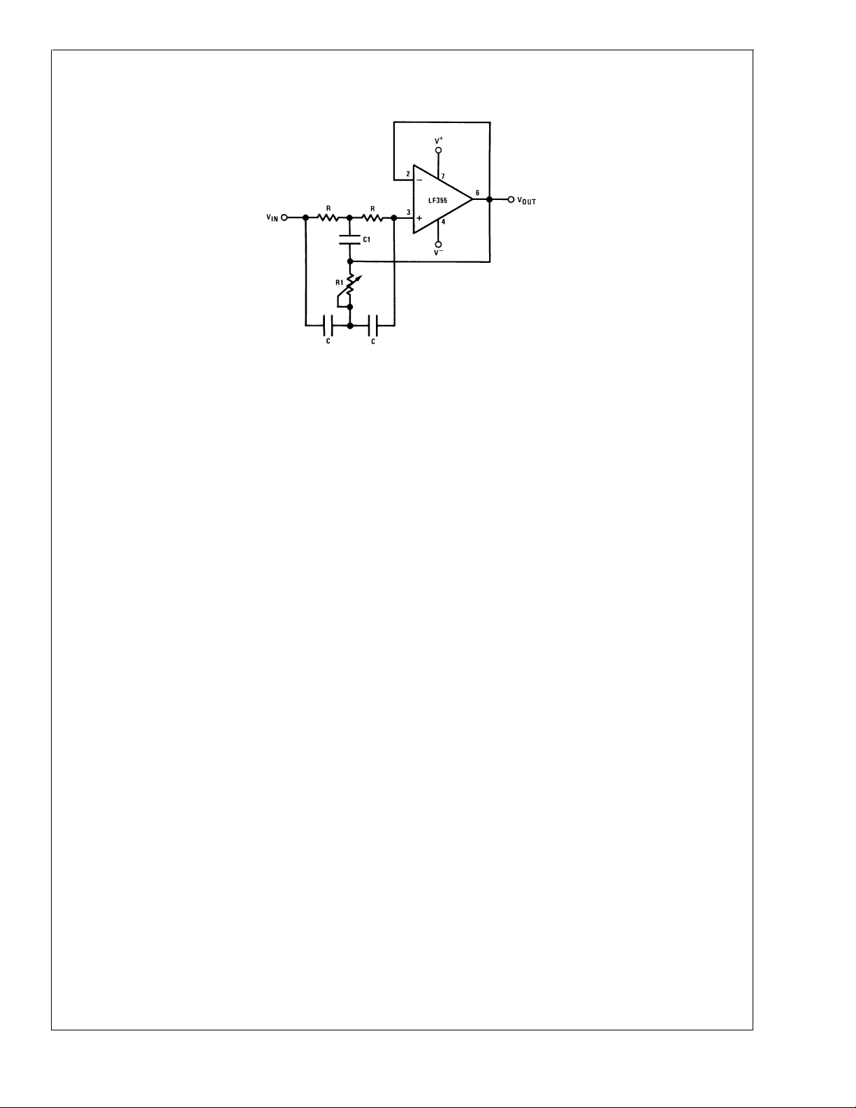
2R1=R=10MΩ
•
2C = C1 = 300pF
Capacitors should be matched to obtain high Q
•
f
•
•
= 120 Hz, notch = −55 dB, Q>100
NOTCH
Use LF155 for
j
Low I
B
j
Low supply current
LF155/LF156/LF256/LF257/LF355/LF356/LF357
High Q Notch Filter
00564634
www.national.com21
Page 22
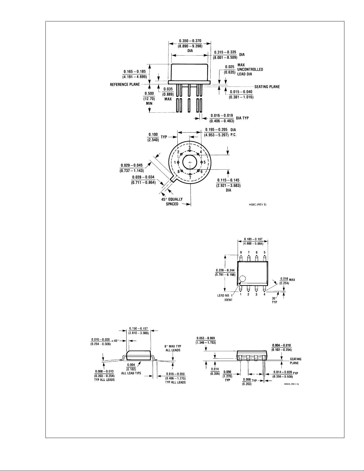
Physical Dimensions inches (millimeters) unless otherwise noted
LF155/LF156/LF256/LF257/LF355/LF356/LF357
Metal Can Package (H)
Order Number LF155H, LF156H, LF256H, LF257H, LF356BH, LF356H or LF357H
NS Package Number H08C
Small Outline Package (M)
Order Number LF356M or LF356MX
NS Package Number M08A
www.national.com 22
Page 23
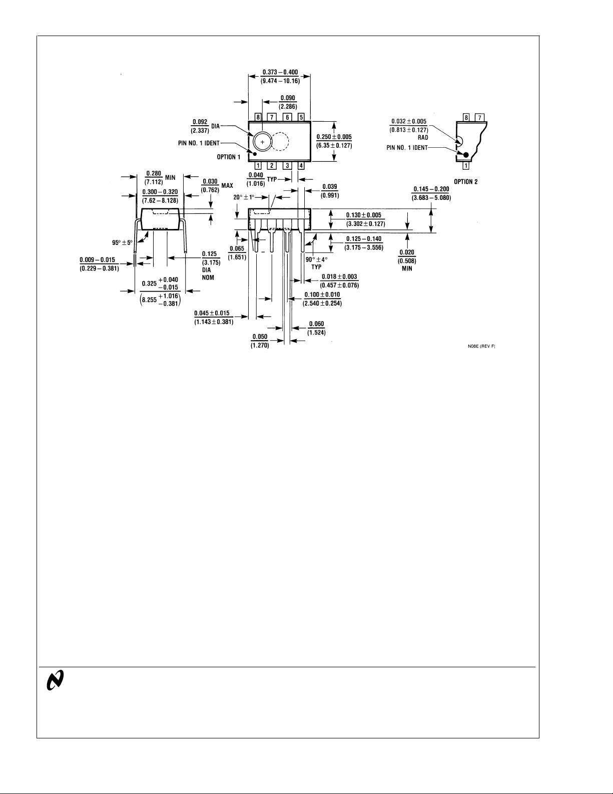
Physical Dimensions inches (millimeters) unless otherwise noted (Continued)
LF155/LF156/LF256/LF257/LF355/LF356/LF357 JFET Input Operational Amplifiers
Molded Dual-In-Line Package (N)
Order Number LF356N
NS Package Number N08E
LIFE SUPPORT POLICY
NATIONAL’S PRODUCTS ARE NOT AUTHORIZED FOR USE AS CRITICAL COMPONENTS IN LIFE SUPPORT
DEVICES OR SYSTEMS WITHOUT THE EXPRESS WRITTEN APPROVAL OF THE PRESIDENT AND GENERAL
COUNSEL OF NATIONAL SEMICONDUCTOR CORPORATION. As used herein:
1. Life support devices or systems are devices or
systems which, (a) are intended for surgical implant
into the body, or (b) support or sustain life, and
whose failure to perform when properly used in
accordance with instructions for use provided in the
2. A critical component is any component of a life
support device or system whose failure to perform
can be reasonably expected to cause the failure of
the life support device or system, or to affect its
safety or effectiveness.
labeling, can be reasonably expected to result in a
significant injury to the user.
National Semiconductor
Corporation
Americas
Email: [email protected]
www.national.com
National does not assume any responsibility for use of any circuitry described, no circuit patent licenses are implied and National reserves the right at any time without notice to change said circuitry and specifications.
National Semiconductor
Europe
Fax: +49 (0) 180-530 85 86
Email: [email protected]
Deutsch Tel: +49 (0) 69 9508 6208
English Tel: +44 (0) 870 24 0 2171
Français Tel: +33 (0) 1 41 91 8790
National Semiconductor
Asia Pacific Customer
Response Group
Tel: 65-2544466
Fax: 65-2504466
Email: [email protected]
National Semiconductor
Japan Ltd.
Tel: 81-3-5639-7560
Fax: 81-3-5639-7507
 Loading...