

Page 1

Philips Semiconductors Linear Products Product specification
LF198/LF298/LF398Sample-and-hold amplifiers
879
August 31, 1994 853-0135 13721
DESCRIPTION
The LF198/LF298/LF398 are monolithic sample-and-hold circuits
which utilize high-voltage ion-implant JFET technology to obtain
ultra-high DC accuracy with fast acquisition of signal and low droop
rate. Operating as a unity gain follower, DC gain accuracy is 0.002%
typical and acquisition time is as low as 6µs to 0.01%. A bipolar
input stage is used to achieve low offset voltage and wide
bandwidth. Input offset adjust is accomplished with a single pin and
does not degrade input offset drift. The wide bandwidth allows the
LF198 to be included inside the feedback loop of 1MHz op amps
without having stability problems. Input impedance of 10
10
Ω allows
high source impedances to be used without degrading accuracy.
P-channel junction FETs are combined with bipolar devices in the
output amplifier to give droop rates as low as 5mV/min with a 1µF
hold capacitor. The JFETs have much lower noise than MOS
devices used in previous designs and do not exhibit high
temperature instabilities. The overall design guarantees no
feedthrough from input to output in the hold mode even for input
signals equal to the supply voltages.
Logic inputs are fully differential with low input current, allowing
direct connection to TTL, PMOS, and CMOS; differential threshold is
1.4V. The LF198/LF298/LF398 will operate from ±5V to ±18V
supplies. They are available in 8-pin plastic DIP, 8-pin Cerdip, and
14-pin plastic SO packages.
FEATURES
•Operates from ±5V to ±18V supplies
•Less than 10µs acquisition time
•TTL, PMOS, CMOS compatible logic input
•0.5mV typical hold step at CH=0.01µF
•Low input offset
•0.002% gain accuracy
•Low output noise in hold mode
•Input characteristics do not change during hold mode
•High supply rejection ratio in sample or hold
•Wide bandwidth
PIN CONFIGURATIONS
FE, N Packages
D
1
Package
NOTE:
1. SO and
non-standard pinouts.
TOP VIEW
TOP VIEW
1
2
3
4 5
6
7
8
1
2
3
4
5
6
7 8
14
13
12
11
10
9
V+
OFFSET VOLTAGE
INPUT
V–
NC
V+
OUTPUT
LOGIC
INPUT
V–
LOGIC REF
NC
NC
NC
NC
NC
LOGIC
LOGIC REFERENCE
OUTPUT
V
OS
Adj
C
h
C
h
APPLICATION
•The LF198/LF298/LF398 are ideally suited for a wide variety of
sample-and-hold applications, including data acquisition,
analog-to-digital conversion, synchronous demodulation, and
automatic test setup
ORDERING INFORMATION
DESCRIPTION TEMPERATURE RANGE ORDER CODE DWG #
8-Pin Ceramic Dual In-Line Package (CERDIP) -55°C to +125°C LF198FE 0580A
14-Pin Plastic Small Outline (SO) Package 0 to +70°C LF398D 0175D
8-Pin Ceramic Dual In-Line Package (CERDIP) 0 to +70°C LF398FE 0580A
8-Pin Plastic Dual In-Line Package (DIP) 0 to +70°C LF398N 0404B
8-Pin Ceramic Dual In-Line Package (CERDIP) -25°C to +85°C LF298FE 0580A
8-Pin Plastic Dual In-Line Package (DIP) -25°C to +85°C LF298N 0404B
Page 2
Philips Semiconductors Linear Products Product specification
LF198/LF298/LF398Sample-and-hold amplifiers
August 31, 1994
880
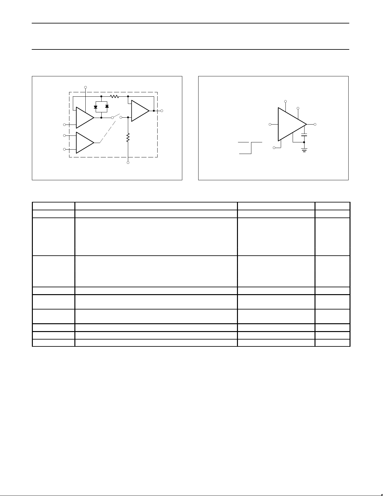
FUNCTIONAL DIAGRAM
OFFSET
INPUT
LOGIC
LOGIC
REFERENCE
HOLD
CAPACITOR
OUTPUT
30k
300
3
8
7
6
5
–
+
TYPICAL APPLICATIONS
OUTPUT
INPUT
LOGIC
ANALOG INPUT
SAMPLE 5V
HOLD 0V
S/H
3
8
7
6
5
4
1
V+
V–
C
h
ABSOLUTE MAXIMUM RATINGS
SYMBOL PARAMETER RATING UNIT
V
S
Supply voltage ±18 V
Maximum power dissipation
T
A
=25°C (still-air)
3
F package 780 mW
N package 1160 mW
D package 1040 mW
T
A
Operating ambient temperature range
LF198 -55 to +125 °C
LF298 -25 to +85 °C
LF398 0 to +70 °C
T
STG
Storage temperature range -65 to +150 °C
V
IN
Input voltage
Equal to
supply voltage
Logic-to-logic reference differential
voltage
2
+7, -30 V
Output short-circuit duration Indefinite
Hold capacitor short-circuit duration 10 sec
T
SOLD
Lead soldering temperature (10sec max) 300 °C
NOTES:
1. The maximum junction temperature of the LF398 is 150°C.
When operating at elevated ambient temperature, the packages must be derated
based on the thermal resistance specified.
2. Although the differential voltage may not exceed the limits given, the common-mode voltage on the logic pins must always be at least 2V
below the positive supply and 3V above the negative supply.
3. Derate above 25°C, at the following rates:
F package at 6.2mW/°C
N package at 9.3mW/°C
D package at 8.3mW/°C
Page 3
Philips Semiconductors Linear Products Product specification
LF198/LF298/LF398Sample-and-hold amplifiers
August 31, 1994
881
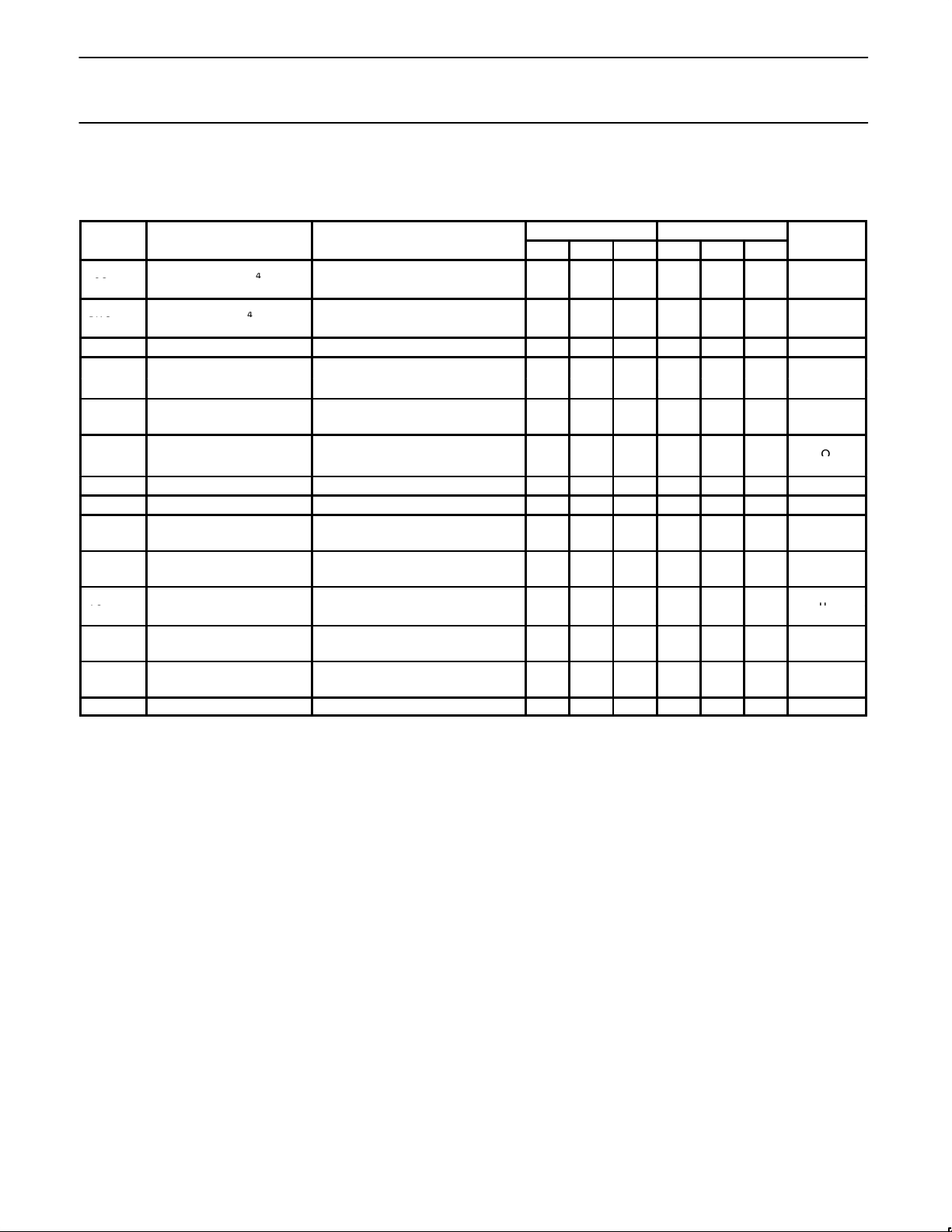
DC ELECTRICAL CHARACTERISTICS
Unless otherwise specified, the following conditions apply: unit is in “sample” mode; V
S
= ±15V; T
J
= 25°C; -11.5V3 V
IN
≤ +11.5V; CH=0.01µF;
and R
L
= 10kΩ. Logic reference voltage = 0V and logic voltage = 2.5V.
LF198/LF298 LF398
SYMBOL
PARAMETER
TEST CONDITIONS
Min Typ Max Min Typ Max
UNIT
TJ=25°C 1 3 2 7
VOSInput offset voltage
4
Full temperature range 5 10
mV
TJ=25°C 5 25 10 50
I
BIAS
Input bias current
4
Full temperature range 75 100
nA
Input impedance TJ=25°C 10
10
10
10
Ω
TJ=25°C, RL=10k
0.002 0.005 0.004 0.01
Gain error
Full temperature range 0.02 0.02
%
Feedthrough attenuation
ratio at 1kHz
TJ=25°C, Ch=0.01µF
86 96 80 90 dB
TJ=25°C, “HOLD“ mode
0.5 2 0.5 4
Output impedance
Full temperature range 4 6
Ω
“HOLD“ step
2
TJ=25°C, Ch=0.01µF, V
OUT
=0 0.5 2.0 1.0 2.5 mV
I
CC
Supply current
4
T
J
≤ 25°C 4.5 5.5 4.5 6.5 mA
Logic and logic reference
input current
T
J
= 25°C 2 10 2 10 µA
Leakage current into hold
capacitor
4
TJ=25°C, “HOLD“ mode 30 100 30 200 pA
∆V
OUT
=10V, Ch=1000pF 4 4
tACAcquisition time to 0.1%
Ch=0.01µF 20 20
µs
Hold capacitor charging
current
VIN-V
OUT
=2V 5 5 mA
Supply voltage rejection
ratio
V
OUT
=0 80 110 80 110 dB
Differential logic threshold TJ=25°C 0.8 1.4 2.4 0.8 1.4 2.4 V
NOTES:
1. Unless otherwise specified, the following conditions apply. Unit is in “sample“ mode, V
S
=±15V, TJ=25°C, -11.5V ≤ V
IN
≤ +11.5V, C
h
= 0.01µF,
and R
L
= 10kΩ. Logic reference voltage = 0V and logic voltage = 2.5V.
2. Hold step is sensitive to stray capacitive coupling between input logic signals and the hold capacitor. 1pF, for instance, will create an
additional 0.5mV step with a 5V logic swing and a 0.01µF hold capacitor. Magnitude of the hold step is inversely proportional to hold
capacitor value.
3. Leakage current is measured at a junction temperature of 25°C. The effects of junction temperature rise due to power dissipation or elevated
ambient can be calculated by doubling the 25°C value for each 11°C increase in chip temperature. Leakage is guaranteed over full input
signal range.
4. The parameters are guaranteed over a supply voltage of ±5 to ±18V.
Page 4
Philips Semiconductors Linear Products Product specification
LF198/LF298/LF398Sample-and-hold amplifiers
August 31, 1994
882
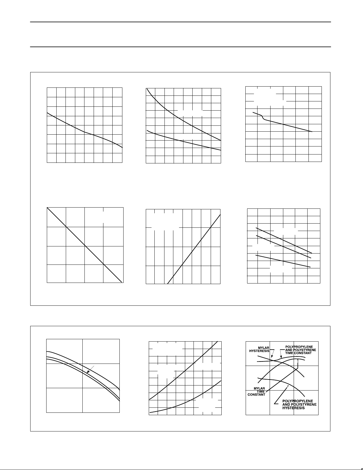
TYPICAL DC PERFORMANCE CHARACTERISTICS
JUNCTION TEMPERATURE (°C)
HOLD STEP (mV)
Input Bias Current Output Short Circuit Current Gain Error
Hold Step
Leakage Current Into
Hold Capacitor
Hold Step Input Voltage
CURRENT (mA)
100
10
1
0.1
0.01
25
20
15
10
5
0
–5
–10
–15
–50 –25 0 25 50 75 100 125 150
JUNCTION TEMPERATURE (°C)
100pF 1000pF
0.01µF 0.1µF 1µF
HOLD CAPACITOR
V+ = V– = 15V
TJ = 25°C
CURRENT (nA) CURRENT (mA)
100
10
1
10
–1
10
–2
–50 –25 0 25 50 75 100 125 150
–50 –25 0 25 50 75 100 125 150
JUNCTION TEMPERATURE (°C)
VS = ±15V
V
OUT
= 0
HOLD MODE
20
18
16
14
12
10
8
6
4
2
0
SOURCING
SINKING
NORMALIZED HOLD STEP AMPLITUDE INPUT VOLTAGE — OUTPUT VOLTAGE (mV)
1
0.8
0.6
0.4
0.2
0
–0.2
–0.4
–0.6
–0.8
–1
–15 –10 –5 0 5 10 15
INPUT VOLTAGE (V)
INPUT VOLTAGE (V)
2
1.8
1.6
1.4
1.2
1
0.8
0.6
0.4
0.2
0
–15 –10 –5 0 5 10 15
TJ = 25°C
TJ = 55°C
TJ = 100°C
TJ = 25°C
RL = 10k
SAMPLE MODE
TYPICAL AC PERFORMANCE CHARACTERISTICS
Acquisition Time Aperture Time Capacitor Hysteresis
TIME ( s)
1
10
100
1000
µ
1%
0.1%
0.01%
V
IN
= 0 TO ±10V
T
J
= 25°C
HOLD CAPACITOR (µF)
0.001 0.01
0.1
250
225
200
175
150
125
100
75
50
25
0
TIME (ns)
V+ = V– = 15V
∆V
OUT
≤ 1mV
NEGATIVE
INPUT
STEP
∆VIN = 10V
POSITIVE
INPUT
STEP
–50 –25 0 25 50 75 100 125 150
JUNCTION TEMPERATURE (°C)
100
10
1
0.1
1001010.1
SAMPLE TIME (ms)
Page 5
Philips Semiconductors Linear Products Product specification
LF198/LF298/LF398Sample-and-hold amplifiers
August 31, 1994
883
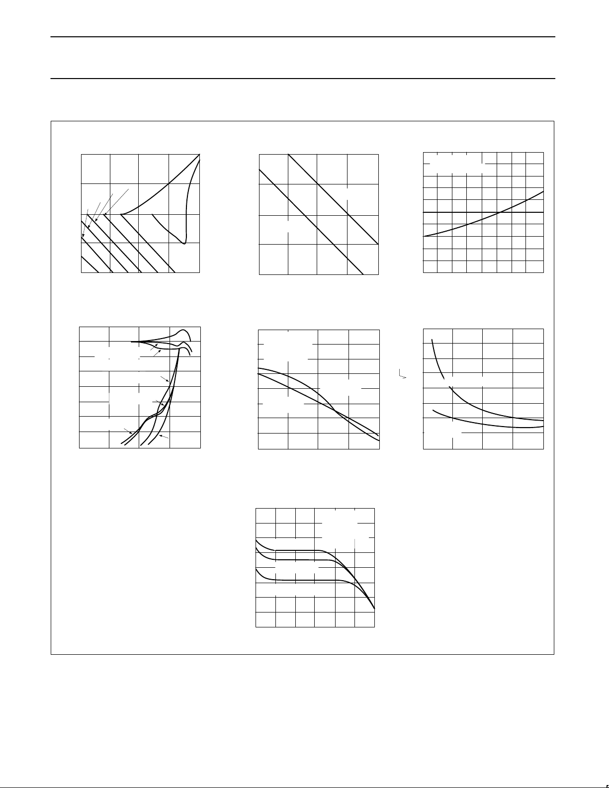
TYPICAL AC PERFORMANCE CHARACTERISTICS (Continued)
Dynamic Sampling Error Output Droop Rate ‘Hold’ Sampling Time
Phase And Gain
(Input to Output, Small-Signal)
Power Supply Rejection Output Noise
Feedthrough Rejection Ratio
(Hold Mode)
ERROR (mV)
100
10
1
–10
–100
0.1 1 10 100 1000
INPUT SLEW RATE (V/ms)
330pF
1000pF
330pF
±
10
0
10
–1
10
–2
10
–3
10
–4
V/ T (V/SEC)∆ ∆
100pF 1000pF 0.01µF 0.1µF 1µF
TJ =25°C
TJ =85°C
HOLD CAPACITOR
V+ = V– = 15V
SETTLING TIME
2
1.8
1.6
1.4
1.2
1
0.8
0.6
0.4
0.2
0
TIME ( s)
µ
–50 –25 0 25 50 75 100 125 150
JUNCTION TEMPERATURE (°C)
160
140
120
100
80
60
40
20
0
10 100 1k 10k 100k
FREQUENCY (Hz)
‘HOLD’ MODE
SAMPLE
MODE
NOISE (nV/ Hz)
NEGATIVE
MODE
POSITIVE
MODE
TJ =25°C
V+ = V– = 15V
V
OUT
= 0°C
160
140
120
100
80
60
40
20
0
100 1k 10k 100k 1M
REJECTION RATIO (dB)
Ch = 1000pF
Ch ≥ 0.01µF
Ch = 1000pF
Ch = 0.01µF
Ch ≥ 0.01µF
Ch = 0
Ch = 0
GAIN — INPUT TO OUTPUT (dB)
5
0
–5
–10
80
70
60
50
40
30
20
10
0
1k 10k 100k 1M 10M
FREQUENCY (Hz)
INPUT TO OUTPUT PHASE DELAY ( )
o
–130
–120
–110
–100
–90
–80
–70
–60
–50
100 1k 10k 100k 1M10010
Ch = 0.01µF
Ch = 1000pF
Ch = 0.1µF
V+ = V– = 15V
TJ =25°C
VIN = 10Vp-p
V
7.8
= 0
RATIO (dB)
FREQUENCY (Hz)
FREQUENCY (Hz)
 Loading...