

Page 1
DEVICES INCORPORATED
LF2301
Image Resampling Sequencer
LF2301
DEVICES INCORPORATED
FEATURES DESCRIPTION
❑❑
❑ 40 MHz Clock Rate
❑❑
❑❑
❑ High-Speed Image Manipulation
❑❑
❑❑
❑ Maximum Image Size: 4096 x 4096
❑❑
Pixels
❑❑
❑ Supports Following Interpolation
❑❑
Algorithms:
• Nearest-Neighbor
• Bilinear Interpolation
• Cubic Convolution
❑❑
❑ Applications:
❑❑
• Video Special-Effects
• Image Recognition
• High-Speed Data Encoding/
Decoding
❑❑
❑ Replaces TRW/Raytheon/Fairchild
❑❑
TMC2301
❑❑
❑ 68-pin PLCC, J-Lead
❑❑
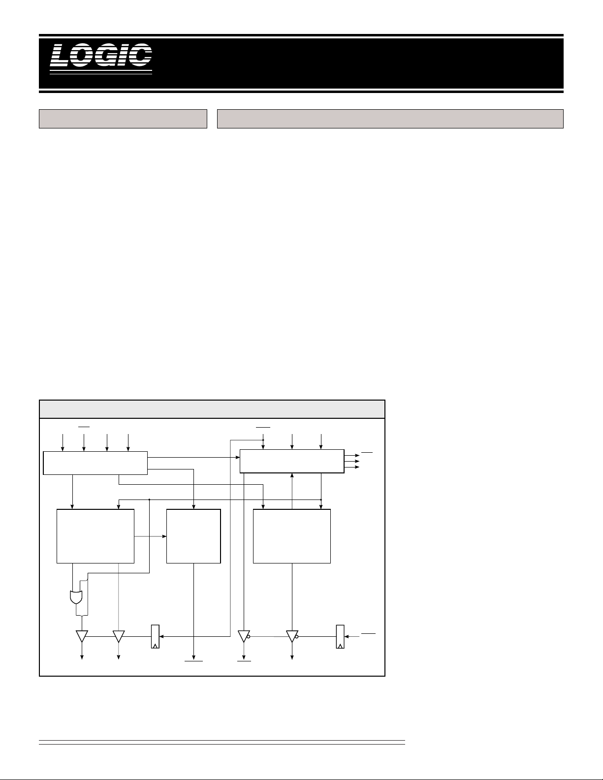
The LF2301 is a self-sequencing
address generator designed to filter
a two-dimensional image or remap
and resample it from one set of
Cartesian coordinates (x,y) into a
new set (u,v).
The LF2301 can resample digitized
images or perform such manipulations as rotation, panning, zooming,
and warping as well as compression
in real-time.
By using two LF2301s in a Image
Transformation System (ITS),
nearest-neighbor, bilinear interpolation, and cubic convolution algorithms, with kernel sizes up to 4 x 4
pixels, are all possible (see Figure 1).
This system can also implement
simple static filters with kernel sizes
up to 16 x 16 pixels.
Image Resampling Sequencer
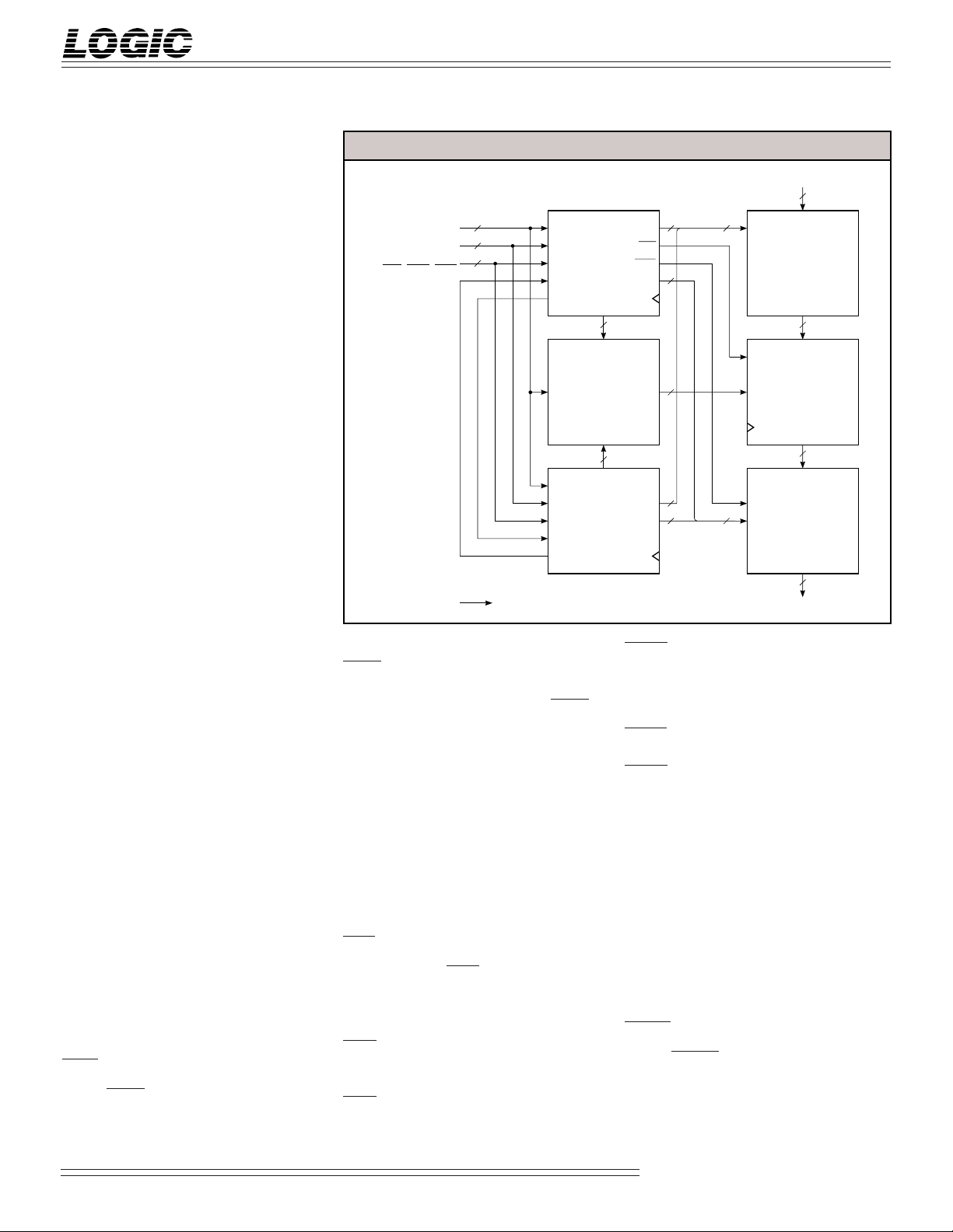
DETAILS OF OPERATION
Most video applications use a pair
of LF2301s in tandem to construct
an ITS. One LF2301 is the row
coordinate generator (x to u) and the
other is the column generator (y to
v). External RAM is needed for
storage of the interpolation coefficient lookup table, as well as for
buffers of the source and destination
images. An external MultiplierAccumulator is required when
performing interpolation or implementing static filters.
The ITS is capable of performing the
general second-order coordinate
transformation of the form:
x(u,v) = Au2+Bu+Cuv+Dv2+Ev+F
y(u,v) = Gu2+Hu+Kuv+Lv2+Mv+N
LF2301 BLOCK DIAGRAM
WENLDR B
3-0P11-0
PARAMETER
STORAGE
SOURCE
ADDRESS
GENERATOR
INTEGERFRACTION
11-0CA7-0
X
INPUT IMAGE
BOUNDARY
COMPARATOR
CZERO
UWRI
INTER INITNOOP
CONTROL
WALK COUNT
TARGET
ADDRESS
GENERATOR
U
11-0
ACC
DONE
END
OETA
where parameters A through N of
the transform are user-defined.
The system steps sequentially
through each pixel in the “target”
image lying within a user-defined
rectangle. For each “target” pixel
at (u,v), the LF2301 points to a
corresponding “source” pixel at
(x,y).
2-1
Video Imaging Products
08/16/2000–LDS.2301-H
Page 2
DEVICES INCORPORATED
LF2301
Image Resampling Sequencer
SIGNAL DEFINITIONS
Power
Vcc and GND
+5V power supply. All pins must be
connected.
Clock
CLK — Master Clock
The rising edge of CLK strobes all
enabled registers.
Inputs
P11-0 — Parameter Register Data Input
P11-0 is the 12-bit Parameter Register
Data input port. P11-0 is latched on
the rising edge of CLK.
B3-0 — Parameter Register Address Input
B3-0 is the 4-bit Parameter Register
Address input port. B3-0 is latched on
the rising edge of CLK.
Outputs
FIGURE 1. IMAGE TRANSFORMATION SYSTEM (ITS)
P
11-0
B
INIT, LDR,
WEN, NOOP, OETA
CLK
12
4
3-0
5
INTER
END
INTERPOLATION
COEFFICIENT
INTER
END
LF2301
Row
Address
Generator
(X)
7-0
CA
8
RAM
8
7-0
CA
LF2301
Column
Address
Generator
(Y)
X
ACC
UWRI
U
Y
V
11-0
11-0
11-0
11-0
12 24
12
12
12
12
IMAGE DATA IN
12
SOURCE
IMAGE
RAM
12
ACC
Y
24
X
LMA1009/2009
12 x 12 bit
Multiplier-
Accumulator
X,Y,P
D
OUT
12
DESTINATION
IMAGE
RAM
12
IMAGE DATA OUT
X11-0 — Source Address Output
X11-0 is the 12-bit registered Source
Address output port.
CA7-0 — Coefficient Address Output
CA7-0 is the 8-bit registered Coefficient Address output port.
U11-0 — Target Address Output
U11-0 is the 12-bit registered Target
Address output port.
Controls
INIT — Initialize
When INIT is HIGH for a minimum of
two clock cycles, the control logic is
cleared and initialized for the start of a
new image transformation. When
INIT goes LOW, normal operation
begins after two clock cycles. INIT is
latched on the rising edge of CLK.
WEN — Write Enable
When WEN is LOW, data latched into
the device on P11-0 is loaded into the
preload register addressed by the data
latched into the device on B3-0. When
WEN is HIGH, data cannot be loaded
into the preload registers and their
contents will not be changed. WEN is
latched on the rising edge of CLK.
LDR — Load Data Register
When LDR is HIGH, data in all
preload registers is latched into the
Transformation Parameter Registers.
When LDR is LOW, data cannot be
loaded into the Transformation
Parameter Registers and their contents
will not be changed. LDR is latched
on the rising edge of CLK.
ACC — Accumulate
The registered ACC output initializes
the accumulation register of the
external multiplier-accumulator. At
the start of each interpolation “walk,”
ACC goes LOW for one cycle effectively clearing the storage register by
loading in only the new first product.
ACC from either the row or column
LF2301 may be used.
UWRI — Target Memory Write Enable
The Target Memory Write Enable goes
LOW for one clock cycle after the end
of each interpolation “walk.” When
OETA is HIGH, this registered output
is forced to the high-impedance state.
UWRI from either the row or column
LF2301 may be used.
INTER — Interconnect
When two LF2301s are used to form
an ITS, the END flag on each device
is connected to INTER on the other
device. The END flag from the row
device indicates an “end of line” to the
column device. The END flag from the
column device indicates a “bottom of
frame” to the row device, forcing a
reset of the address counter.
NOOP — No Operation
When NOOP is LOW, the clock is
overridden holding all address
generators in their current state. X11-0
and CA7-0 are forced to the high-
2-2
Video Imaging Products
08/16/2000–LDS.2301-H
Page 3

DEVICES INCORPORATED
LF2301
Image Resampling Sequencer
impedance state. Users may then
access external memory. Normal
operation resumes on the next clock
cycle after NOOP goes HIGH. NOOP
is latched on the rising edge of CLK.
OETA — Target Memory Output Enable
When OETA is HIGH, UWRI and U11-0
are forced to the high-impedance
state. When OETA is LOW, UWRI
and U11-0 are enabled on the next
clock cycle. OETA is latched on the
rising edge of CLK.
Flags
CZERO — Coefficient Zero
If in a row device x<0,
XMIN≤x≤XMAX, or x≥4096, the
registered CZERO flag goes HIGH . If
0≤x<XMIN or XMAX<x<4096, CZERO
goes LOW. In an ITS, when the source
address falls outside a rectangle with
vertices (XMIN, YMIN), (XMAX,
YMIN), (XMIN, YMAX), and (XMAX,
YMAX), the logical AND of the
CZERO flags from the row and
column of the LF2301s will go LOW
representing an invalid address.
END — End of Row/Frame
When two LF2301s are used to form
an ITS, the END flag on each device
is connected to INTER on the other
device. The END flag from the row
device indicates an “end of line” to the
column device. The END flag from
the column device indicates a “bottom
of frame” to the row device, forcing a
reset of the address counter.
When Mode is set to “00” or “10”
END goes HIGH on the row device
for (K+1) x (K+1) clock cycles
starting[2 x (K+1) x (K+1)] + 1 clock
cycles before the last X address of a
row. END goes HIGH on the column
device for (K+1)3 x (UMAX-UMIN)
clock cycles starting at (K+1)3 x
(UMAX-UMIN) + 1 clock cycles before
the last X address of a frame.
When Mode is set to “01” or “11”
END goes HIGH on the row device
for K+1 clock cycles starting at (K+1) +
2 clock cycles before the last X address
of a row. END goes HIGH on the
column device for (K+1) x (K+1)
clock cycles starting at [(K+1) x (K+1)] +
1 clock cycles before the last X address
of a frame.
DONE — End of Transform
In a two LF2301 system, after the last
walk of the last row of an image, the
registered DONE flag goes HIGH
indicating the end of the transform.
DONE goes HIGH one clock cycle
before the last X address of a frame. If
AIN is HIGH, DONE will remain
HIGH for one clock cycle. If AIN is
LOW, DONE will remain HIGH until
a new transform begins.
Transformation Control Parameters
XMIN, XMAX, YMIN, YMAX
XMIN, XMAX, YMIN, YMAX define
the valid area in the source image
from which pixels may be read. The
CZERO flags will denote a valid
memory read whenever the LF2301s
generate an (x,y) address within this
boundary.
UMIN, UMAX, VMIN, VMAX
UMIN, UMAX, VMIN, VMAX define
the area in the destination image into
which pixels will be written.
(UMIN, VMIN) is the top left corner
and (UMAX + 1, VMAX) is the bottom
right corner. The following conditions
must be met: UMAX>UMIN and
VMAX>VMIN.
x0, y0
x0, y0 determine what the first pixel read
out of the source image will be at the
beginning of an image transformation.
x0, y0 will be the upper left corner of the
original image in non-inverting, nonreversing applications.
dx/du
dx/du is the displacement along the
x axis corresponding to a one-pixel
movement along the u axis.
2-3
dx/dv
dx/dv is the displacement along the
x axis corresponding to each one-pixel
movement along the v axis.
dy/du
dy/du is the displacement along the
y axis corresponding to each one-pixel
movement along the u axis.
dy/dv
dy/dv is the displacement along the
y axis corresponding to each one-pixel
movement along the v axis.
2
d2x/du
d2x/du2 determines the rate of change
of dx/du with each step along a line
in the output image.
2
d2x/dv
d2x/dv2 determines the rate of change
of dx/dv with each step down a
column in the output image.
2
d2y/du
d2y/du2 determines the rate of change
of dy/du with each step along a line
in the output image.
2
d2y/dv
d2y/dv2 determines the rate of change
of dy/dv with each step down a
column in the output image.
d2x/dudv
d2x/dudv determines the rate of
change of dx/du while moving
vertically through the output image.
d2x/dudv also determines the rate of
change of dx/dv while moving
horizontally through the output
image.
d2y/dudv
d2y/dudv determines the rate of
change of dy/dv while moving
horizontally through the output
image. d2y/dudv also determines the
rate of change of dy/du while
moving vertically through the output
image.
Video Imaging Products
08/16/2000–LDS.2301-H
Page 4
DEVICES INCORPORATED
LF2301
Image Resampling Sequencer
TABLE 1. MODE SELECTION
M1 M0 MODE
0 0 single-pass operation (CW)
0 1 pass 1 of two-pass operation
1 0 single-pass operation (CCW)
1 1 pass 2 of two-pass operation
R/C — Row/Column Select
When set to 0, the LF2301 functions as
a row device. When set to 1, the
LF2301 functions as a column device.
M1-0 — Mode
This 2-bit control word defines four
modes as follows (see table 1):
The 1st and 3rd modes are singlepass operations where the device
walks through a (K + 1) x (K + 1)
kernel for each output pixel. K is the
kernel size determined by K3-0 in
Parameter Register 7. In mode 00, the
spiral walk is in the clockwise direction. In mode 10, the spiral walk is in
the counter clockwise direction.
The 2nd and 4th modes are used
together to perform a two-pass
operation. The first pass (mode 01)
performs a (K+1) kernel in the
horizontal dimension. The second
pass (mode 11) performs a (K+1)
kernel in the vertical dimension.
The result of pass 1 is stored in the
destination image memory and is used
as the source image data for the second
pass. A system to switch source and
destination memory banks could be
designed, or utilization of a second
LF2301 pair in a pipelined architecture
could be used. In this case, the system
would require a third image buffer for
the final destination image.
K3-0 — Kernel
Kernel determines the length of the
spiral walk when performing image
transformations and the size of the
filter when implementing static filters
(see table 2). When performing image
transformations, the longest spiral walk
possible is 4 x 4 pixels (Kernel = 3). For
static filters, kernels of up to 16 x 16
pixels (Kernel = 15) are possible.
FOV — Field of View
FOV determines the distance between
pixels in a spiral walk. An FOV of 1
means each step in a spiral walk is one
pixel. An FOV of 2 means each step is
two pixels, and so on. FOV can be set
as high as 7 (see Table 3). It is important to note when FOV is 0, the x and
y addresses will not change during a
spiral walk. They will remain fixed at
the first pixel address of the spiral
walk.
ALR — Autoload
When set HIGH and upon INIT being
strobed, the LDR control is automatically
asserted which causes the data
currently stored in the Preload Registers
to be loaded into the Transformation
Parameter Registers.
AIN — Autoinit
A new transform automatically begins
if the AIN bit is HIGH when the end of
an image is reached. The DONE flag
will go HIGH for one clock cycle. If
AIN is LOW, UWRI and the DONE flag
remain HIGH until the user strobes the
INIT control to begin a new image
transformation.
PIPE — Pipe Control
In order to compensate for buffered
source image RAM, PIPE adjusts the
timing of UWRI and ACC. If the PIPE
bit is HIGH, UWRI and ACC will have
a one clock cycle delay added relative
to the generation of the target address.
TM — Test Mode
Calculations of the source image and
coefficient addresses are made by an
internal 28-bit accumulator. TM
allows access to the sign bit and the
seven bits below the four coefficient
address bits in the accumulator. When
TM is HIGH the sign bit and 11 bits
below the source image address are fed
to X11-0 (see Figure 2). When TM is
LOW, the source image address is fed
to X11-0. Two clock cycles are required
to access both the MS and LS words of
the internal accumulator.
Functional Description
The LF2301 is an address generator
designed to be used in an image
transformation system (ITS). When
implementing an LF2301-based ITS,
second-order image transformations
can be performed like resampling,
rotation, warping, panning, and
rescaling, all at real-time video rates.
2D filtering operations, like pixel
convolutions, can also be performed.
In most applications two LF2301s are
used, one to generate the row addresses
and the other to generate the column
TABLE 2. KERNEL
K3 K2 K1 K0 Kernel
00 00 1 x 1
00 01 2 x 2
00 10 3 x 3
00 11 4 x 4
01 00 5 x 5
01 01 6 x 6
01 10 7 x 7
01 11 8 x 8
10 00 9 x 9
10 0110 x 10
10 1011 x 11
10 1112 x 12
11 0013 x 13
11 0114 x 14
11 1015 x 15
11 1116 x 16
TABLE 3. FIELD OF VIEW
F2 F1 F0 FOV
000 0
001 1
010 2
011 3
100 4
101 5
110 6
111 7
2-4
Video Imaging Products
08/16/2000–LDS.2301-H
Page 5
DEVICES INCORPORATED
LF2301
Image Resampling Sequencer
addresses. An example of an ITS
implemented with two LF2301s is
shown in Figure 1. In this system the
following components are used: two
LF2301s, a multiplier-accumulator
(MAC), interpolation coefficient RAM,
and source/target image RAM.
Maximum image size is 4096 x 4096
pixels. Data word size is determined
by the word size of the external RAM.
A typical ITS performs image transformations as follows:
a. The LF2301s generate sequential
pixel addresses (left to right, top to
bottom) which fill the rectangle in the
target image RAM defined by
(UMIN,VMIN) and (UMAX +1, VMAX).
It is important to note that the U value
of the last pixel address on each line of
the target RAM is UMAX + 1.
b. The LF2301s calculate the address
of the corresponding pixel in the
source image RAM for each target
pixel address generated.
c. If interpolation is needed, the
external MAC sums the products of
the source pixels and the interpolation coefficients. Control signals for
the MAC and address signals for the
interpolation coefficient RAM are
provided by the LF2301s.
FIGURE 2. TEST MODE DATA ROUTING
28-BIT INTERNAL
ACCUMULATOR
SIGN
WALK COUNTER
1
12
4
7
12
12
4
4
FIGURE 3. ADDRESS TRANSFORMATION EQUATIONS
+
+
+=x
0
FOV CAX(w)·
+=y
0
FOV CAY(w)·
dx
du
dy
du
m+ n+ mn+ +x
m+ n+ mn+ +y
dx
dv
+
FOV m CAX(ker)·
dy
dv
FOV m CAY(ker)·+·
·
2
d x
dudv
2
d y
dudv
2
d x
du
2
d y
du
2
2
m – m
m – m
X11-0/T11-0
CA7-4
CA3-0
2
2
2
2
2
d x
dv
2
d y
dv
2
n – n
2
2
2
n – n
2
2
d. The new pixel value is written into
the target image RAM.
The LF2301s generate source pixel
addresses according to the following
general second order equations:
x = Au2 + Bu + Cuv + Dv2 + Ev + F
y = Gu2 + Hu + Kuv + Lv2 + Mv + N
where (x,y) and (u,v) are the source
and target coordinates respectively.
A through N are user-defined parameters. The actual second order equations used are shown in Figure 3.
UMIN
VMIN
NOTE:
m=u
+
n=v
+
2
m – m
2
APPROXIMATES THEEXPONENTIAL CHARACTERISTIC OF
Video Imaging Products
2-5
2
m
.
08/16/2000–LDS.2301-H
Page 6
DEVICES INCORPORATED
LF2301
Image Resampling Sequencer
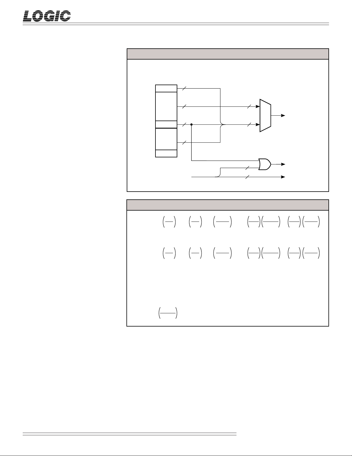
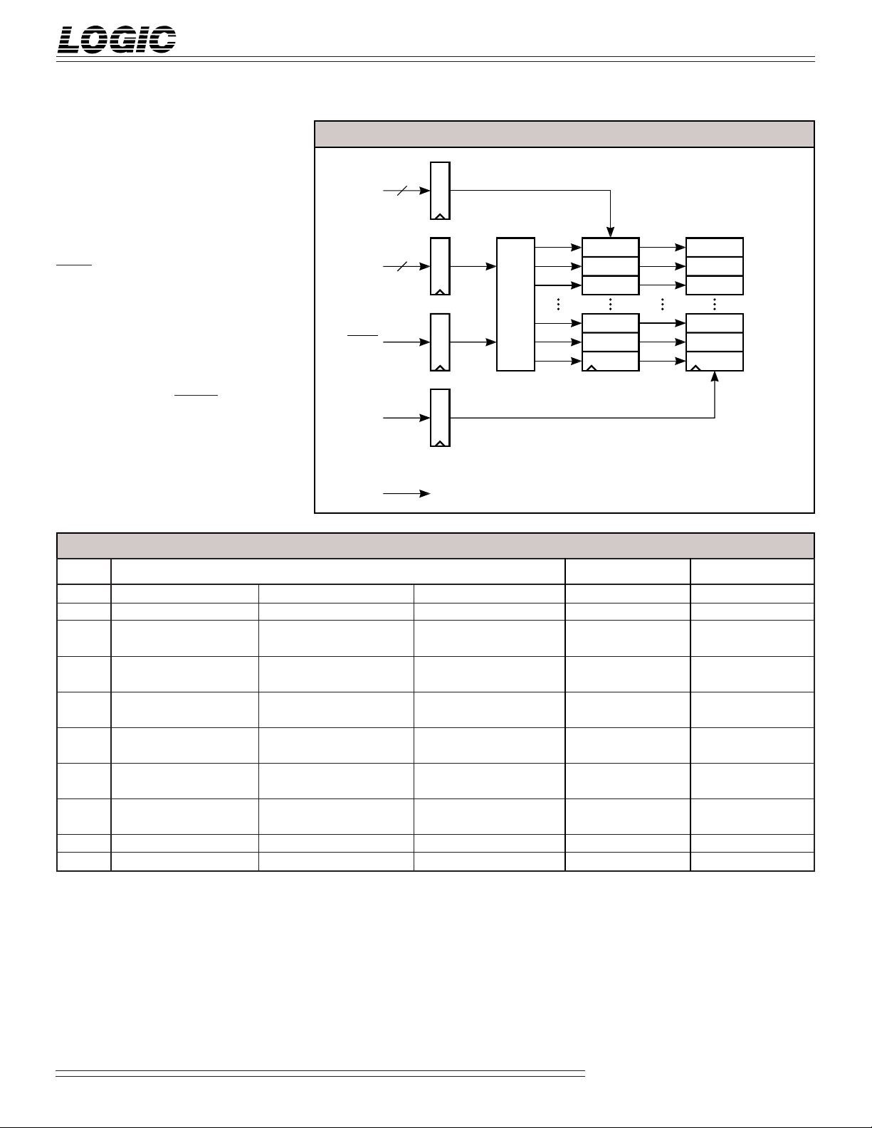
Transformation Parameter Register
Loading
The LF2301 allows Transformation
Parameters to be updated on-the-fly.
The loading of these registers is
double-buffered (see Figure 4). Any
or all of the first level registers can
be loaded using P11-0, B3-0, and
WEN without affecting the parameters currently in use.
LDR simultaneously updates all
Transformation Parameter Registers.
If Autoload (ALR) is active, these
registers will be updated automatically at the beginning of each new
image. Note that NOOP does not
affect the loading of the Transformation Parameter Registers.
FIGURE 4. LDR CONTROL FOR PARAMETER UPDATE
P11-0
3-0
B
WEN
LDR
CLK
12
4
C15
C14
C13
DECODE
C2
C1
C0
PRELOAD
REGISTERS
TRANSFORMATION
PARAMETER
REGISTERS
TABLE 4. PARAMETER REGISTER FORMATS (ROW OR COLUMN MODE)
ADDR MSB FORMAT LSB ROW COLUMN
10
9
8
7
6
5
4
3
2
1
0000 2112
0001 2112
0010 262
2
2
2
10
9
2
5
2
8
2
4
3
2
2
7
2
2
6
2
2
1
2
0011 ALR AIN PIPE R/C M1 M0 –2
–2
–3
–4
–5
0100 2–12
2
2
2
0101 TM F2 F1 F0 –2
–2
–3
0110 2–12
2
–4
2
2
0111 K 3 K2 K1 K0 –272
1000 2–92
1001 –232
1010 2–92
1011 –232
1100 2–92
1101 –232
1110 2112
1111 2112
–102–112–122–132–142–152–162–172–182–192–20
2
1
2
–102–112–122–132–142–152–162–172–182–192–20
2
2
–102–112–122–132–142–152–162–172–182–192–20
2
2
10
2
10
2
0
2
2
1
0
2
2
1
0
2
9
9
2
8
2
2
8
2
2
–6
2
7
6
2
–5
–6
2
6
–1
–2
2
–1
–2
2
–1
–2
2
7
6
2
7
6
2
2
2
2
2
5
4
2
2
0
2
2
12
2
–7
2
2
5
2
2
–7
2
2
5
2
2
–3
2
2
–3
2
2
–3
2
2
5
2
2
5
2
2
3
2
–1
–2
2
11
10
2
–8
–9
2
4
3
2
–8
–9
2
4
3
2
–4
–5
2
–4
–5
2
–4
–5
2
4
3
2
4
3
2
2
2
2
2
–3
2
2
9
2
2
–102–112–12
2
2
2
2
–102–112–12
2
2
2
2
–6
2
2
–6
2
2
–6
2
2
2
2
2
2
2
2
0
2
1
0
2
–4
–5
2
8
7
2
XMIN YMIN
XMAX YMAX
x0 (LS) y0 (LS)
Controls, x0 (MS) Controls, y0 (LS)
dx/du (LS) dy/du (LS)
1
20Controls, dx/du (MS) Controls, dy/du (MS)
dx/dv (LS) dy/dv (LS)
1
0
2
Kernel, dx/dv (MS) Kernel, dy/dv (MS)
d2x/dudv (LS) d2y/dudv (LS)
–7
–8
2
d2x/dudv (MS) d2y/dudv (MS)
d2x/du2 (LS) d2y/du2 (LS)
–7
–8
2
d2x/du2 (MS) d2y/du2 (MS)
d2x/dv2 (LS) d2y/dv2 (LS)
–7
–8
2
1
0
2
1
0
2
d2x/dv2 (MS) d2y/dv2 (MS)
UMIN VMIN
UMAX VMAX
2-6
Video Imaging Products
08/16/2000–LDS.2301-H
Page 7

DEVICES INCORPORATED
1 = 1st pixel of 1st spiral walk,
2 = 1st pixel of 2nd spiral walk, etc.
4
6789
5
6
7
8
12
5
LF2301
Image Resampling Sequencer
Static Filter
Static filtering at real-time video
rates can be performed as shown in
Figure 5. This mode is selected by
loading M1-0 with “00” for a clockwise spiral walk. A counterclockwise spiral walk could be selected
by loading M1-0 with “10.” In this
example, a static filter with a kernel
size of 3 x 3 pixels is desired. Loading K3-0 with “0010” selects a kernel
size of 3 x 3. The first pixel selected
is determined by x0 and y0. In this
example, the first pixel is (6,6). In
this case, the LF2301s should address consecutive pixels during each
spiral walk. For this to occur, FOV
must be set to 1 (F2-0 loaded with
“001”).
After the last pixel of a spiral walk
has been selected, the next pixel
address is determined by adding
dx/du to the current X address and
by adding dy/du to the current Y
address (unless the kernel just
completed was the last for that line).
At the end of the first spiral walk,
pixel (7,5) is addressed. Since the
first pixel of the next spiral walk
should be (7,6), dx/du is selected to
be 0 and dy/du is selected to be 1.
After the last pixel of the last spiral
walk on the first line has been
selected, the first pixel address of
the second line is determined by
adding dx/dv to x0 and by adding
dy/dv to y0. Since the first pixel of
the first spiral walk on the second
line should be (6,7), dx/dv is
selected to be 0 and dy/dv is selected to be 1. Second order differential terms are not used in this
filter and are therefore set to 0.
UMIN and VMIN are both selected
to be 6. UMAX and VMAX are both
selected to be 7. Table 5 shows the
values loaded into all Parameter
Registers. Table 6 shows the ITS
outputs for the 3 x 3 static filter.
FIGURE 5. 3
××
× 3 STATIC FILTER
××
TABLE 5. PARAMETER REGISTERS
ADDR Row (HEX) Column (HEX)
0000 000 000
0001 FFF FFF
0010 0C0 0C0
0011 000 100
0100 000 000
0101 100 101
0110 000 000
0111 200 201
1000 000 000
1001 000 000
1010 000 000
1011 000 000
1100 000 000
1101 000 000
1110 006 006
1111 007 007
2-7
Video Imaging Products
08/16/2000–LDS.2301-H
Page 8

DEVICES INCORPORATED
LF2301
Image Resampling Sequencer
TABLE 6. ITS OUTPUTS FOR 3
Cycle x y CAx (HEX) CAy (HEX) u v INIT ACC UWRI ENDxENDyDONE
1 66 00 00 xx101000
2 66 00 00 xx001000
3 66 00 00 xx001000
4 66 00 00 xx001000
5 76 01 01 xx010000
6 77 02 02 xx011000
7 67 03 03 xx011000
8 57 04 04 xx011000
9 56 05 05 xx011000
10 55 06 06 xx011000
11 65 07 07 xx011100
12 75 08 08 xx011100
13 76 00 00 66001100
14 86 01 01 66010100
15 87 02 02 66011100
16 77 03 03 66011100
17 67 04 04 66011100
18 66 05 05 66011100
19 65 06 06 66011100
20 75 07 07 66011000
21 85 08 08 66011000
22 86 00 00 76001000
23 96 01 01 76010000
24 97 02 02 76011000
25 87 03 03 76011000
26 77 04 04 76011000
27 76 05 05 76011000
28 75 06 06 76011000
29 85 07 07 76011010
30 95 08 08 76011010
31 67 00 00 86001010
32 77 01 01 86010010
33 78 02 02 86011010
34 68 03 03 86011010
35 58 04 04 86011010
36 57 05 05 86011010
37 56 06 06 86011010
38 66 07 07 86011110
39 76 08 08 86011110
40 77 00 00 67001110
41 87 01 01 67010110
42 88 02 02 67011110
43 78 03 03 67011110
44 68 04 04 67011110
45 67 05 05 67011110
46 66 06 06 67011110
47 76 07 07 67011010
48 86 08 08 67011010
49 87 00 00 77001010
50 97 01 01 77010010
51 98 02 02 77011010
52 88 03 03 77011010
53 78 04 04 77011010
54 77 05 05 77011010
55 76 06 06 77011010
56 86 07 07 77011001
57 96 08 08 77011001
58 66 00 00 87001001
××
× 3 STATIC FILTER
××
2-8
Video Imaging Products
08/16/2000–LDS.2301-H
Page 9

DEVICES INCORPORATED
1,2
34
5
0123
1
2
3
4
1 = 1st pixel of 1st spiral walk,
calculated pixels
0
-1
source image pixels
2 = 1st pixel of 2nd spiral walk, etc.
LF2301
Image Resampling Sequencer
Image Rotation & Bilinear Interpolation
Figure 8 shows an example of rotating
an image 30º and using bilinear
interpolation. This mode is selected by
loading M1-0 with “00” for a clockwise
spiral walk. A counterclockwise spiral
walk could be selected by loading M1-0
with “10.” Bilinear interpolation
requires a kernel size of 2 x 2 pixels.
Loading K3-0 with “0001” selects a
kernel size of 2 x 2. The first pixel
selected is determined by x0 and y0. In
this example, the first pixel is (0,0). In
this case, the LF2301s should address
consecutive pixels during each spiral
walk. For this to occur, FOV must be
set to 1 (F2-0 loaded with “001”).
After the last pixel of a spiral walk has
been selected, the next pixel address is
determined by adding dx/du to the
current X address and by adding
dy/du to the current Y address
(unless the kernel just completed was
the last for that line). At the end of the
first spiral walk, pixel (0,1) is addressed. Since the next calculated
pixel should be (0.866,0.5), dx/du is
selected to be 0.866 and dy/du is
selected to be 0.5. However, after
adding dx/du and dy/du to the X
and Y addresses respectively, the
generated address is (0.866,1.5). The Y
address is off by a value of 1. This is
due to the fact that the last pixel
address of a spiral walk is used to
calculate the first pixel address of
the next spiral walk. In order for the
LF2301s to generate the correct result,
dy/du must be modified by subtracting a 1 from it. The correct value of
dy/du is -0.5. Figure 6 shows how the
unmodified differential terms were
calculated.
After the last pixel of the last spiral
walk on the first line has been selected,
the first pixel address of the second
line is determined by adding dx/dv to
x0 and by adding dy/dv to y0. Since
the first calculated pixel of the first
spiral walk on the second line should
be (-0.5,0.866), dx/dv is selected to
be -0.5 and dy/dv is selected to be
0.866. Second order differential terms
are not used in this transform and are
therefore set to 0.
It is important to note that the integer
portion of the address generated in
the LF2301 is used as the X or Y
pixel address. The fractional portion
(sub-pixel portion) is used as the
coefficient RAM address.
UMIN and VMIN are both selected to
be 0. UMAX and VMAX are both
selected to be 2. Table 7 shows the
values loaded into all Parameter
Registers. Table 8 shows the ITS
outputs for this example.
FIGURE 6. DIFFERENTIAL TERMS
dx
= cos 30º
= 0.866
du
dy
=
sin 30º = 0.5
du
dx
=
–sin 30º = –0.5
dv
dy
cos 30º = 0.866
=
dv
FIGURE 7. 30
dy
dv
°°
° IMAGE ROTATION
°°
dx
dv
dx
du
length =1
30º
x
dy
du
u
v
source image pixels
calculated pixels
y
FIGURE 8. 30
°°
° IMAGE ROTATION
°°
TABLE 7. PARAMETER REGISTERS
ADDR Row (HEX) Column (HEX)
0000 000 000
0001 FFF FFF
0010 000 000
0011 000 100
0100 DDB 800
0101 100 1FF
0110 800 DDB
0111 1FF 100
1000 000 000
1001 000 000
1010 000 000
1011 000 000
1100 000 000
1101 000 000
1110 000 000
1111 002 002
2-9
Video Imaging Products
08/16/2000–LDS.2301-H
Page 10

DEVICES INCORPORATED
LF2301
Image Resampling Sequencer
TABLE 8. ITS OUTPUTS FOR 30
Cycle x y CAx (HEX) CA
1 00 00 00 xx101000
2 00 00 00 xx001000
3 00 00 00 xx001000
4 00 00 00 xx001000
5 10 01 01 xx010000
6 11 02 02 xx011000
7 01 03 03 xx011000
8 00 D0 80 00001000
9 10 D1 81 00010000
10 11 D2 82 00011100
11 01 D3 83 00011100
12 11 B0 00 10001100
13 21 B1 01 10010100
14 22 B2 02 10011000
15 12 B3 03 10011000
16 21 90 80 20001000
17 31 91 81 20010000
18 32 92 82 20011000
19 22 93 83 20011000
20 -10 80 D0 30001000
21 00 81 D1 30010000
22 01 82 D2 30011000
23 -11 83 D3 30011000
24 01 50 50 01001000
25 11 51 51 01010000
26 12 52 52 01011100
27 02 53 53 01011100
28 11 30 D0 11001100
29 21 31 D1 11010100
30 22 32 D2 11011000
31 12 33 D3 11011000
32 22 10 50 21001000
33 32 11 51 21010000
34 33 12 52 21011010
35 23 13 53 21011010
36 -11 00 B0 31001010
37 01 01 B1 31010010
38 02 02 B2 31011010
39 -12 03 B3 31011010
40 -12 D0 30 02001010
41 02 D1 31 02010010
42 03 D2 32 02011110
43 -13 D3 33 02011110
44 02 B0 B0 12001110
45 12 B1 B1 12010110
46 13 B2 B2 12011010
47 03 B3 B3 12011010
48 13 90 30 22001010
49 23 91 31 22010010
50 24 92 32 22011001
51 14 93 33 22011001
52 00 00 00 32001001
53 10 01 01 32010001
54 11 02 02 32011001
55 01 03 03 32011001
°°
° IMAGE ROTATION WITH BILINEAR INTERPOLATION
°°
(HEX) u v INIT ACC UWRI END
y
ENDyDONE
x
2-10
Video Imaging Products
08/16/2000–LDS.2301-H
Page 11

DEVICES INCORPORATED
LF2301
Image Resampling Sequencer
Pass 1 of Two-Pass Operation
Pass 1 of the two-pass operation
performs horizontal filtering on an
image as shown in Figure 9. This
mode is selected by loading M1-0 with
“01.” In this example, a horizontal
filter with a kernel size of 3 pixels is
desired. Loading K3-0 with “0010”
selects a kernel size of 3. The first
pixel selected is determined by x0 and
y0. In this example, the first pixel is
(0,0). In this case, the LF2301s should
address consecutive pixels during each
pixel walk. For this to occur, FOV must
be set to 1 (F2-0 loaded with “001”).
After the last pixel of a pixel walk has
been selected, the next pixel address is
determined by adding dx/du to the
current X address and by adding dy/
du to the current Y address (unless the
kernel just completed was the last for
that line). At the end of the first pixel
walk, pixel (2,0) is addressed. Since
the first pixel of the next pixel walk
should be (1,0), dx/du is selected to be
-1 and dy/du is selected to be 0. After
the last pixel of the last pixel walk on
the first line has been selected, the first
FIGURE 9. PASS 1 OF TWO-PASS
0
-1
0
1
2
3
1 = 1st pixel of 1st walk,
2 = 1st pixel of 2nd walk, etc.
pixel address of the second line is
determined by adding dx/dv to x0
and by adding dy/dv to y0. Since the
first pixel of the first pixel walk on the
second line should be (0,1), dx/dv is
selected to be 0 and dy/dv is selected
to be 1. Second order differential
terms are not used in this filter and are
therefore set to 0.
1234
123
645
7
TABLE 9. PARAMETER REGISTERS
ADDR Row (HEX) Column (HEX)
0000 000 000
0001 FFF FFF
0010 000 000
0011 040 140
0100 000 000
0101 1FF 000
0110 000 000
0111 200 201
1000 000 000
1001 000 000
1010 000 000
1011 000 000
1100 000 000
1101 000 000
1110 005 005
1111 006 006
UMIN and VMIN are both selected to
be 5. UMAX and VMAX are both
selected to be 6. Table 9 shows the
values loaded into all Parameter
Registers. Table 10 shows the ITS
outputs for the Pass 1 of a Two-Pass
operation.
TABLE 10. ITS OUTPUTS FOR PASS 1 OF TWO-PASS
Cycle x y CAx (HEX) CAy (HEX) u v INIT ACC UWRI ENDxENDyDONE
1 00 00 00 xx101000
2 00 00 00 xx001000
3 00 00 00 xx001000
4 00 00 00 xx001000
5 10 01 01 xx010100
6 20 02 02 xx011100
7 10 00 00 55001100
8 20 01 01 55010000
9 30 02 02 55011000
10 20 00 00 65001000
11 30 01 01 65010010
12 40 02 02 65011010
13 01 00 00 75001010
14 11 01 01 75010110
15 21 02 02 75011110
16 11 00 00 56001110
17 21 01 01 56010010
18 31 02 02 56011010
19 21 00 00 66001010
20 31 01 01 66010001
21 41 02 02 66011001
22 00 00 00 76001001
23 10 01 01 76010101
24 20 02 02 76011101
2-11
Video Imaging Products
08/16/2000–LDS.2301-H
Page 12

DEVICES INCORPORATED
LF2301
Image Resampling Sequencer
Pass 2 of Two-Pass Operation
Pass 2 of the two-pass operation
performs vertical filtering on an image
as shown in Figure 10. This mode is
selected by loading M1-0 with “11.” In
this example, a vertical filter with a
kernel size of 3 pixels is desired.
Loading K3-0 with “0010” selects a
kernel size of 3. The first pixel selected is determined by x0 and y0. In
this example, the first pixel is (0,0). In
this case, the LF2301s should address
consecutive pixels during each pixel
walk. For this to occur, FOV must be
set to 1 (F2-0 loaded with “001”).
After the last pixel of a pixel walk has
been selected, the next pixel address
is determined by adding dx/du to the
current X address and by adding
dy/du to the current Y address
(unless the kernel just completed was
the last for that line). At the end of
the first pixel walk, pixel (0,2) is
addressed. Since the first pixel of the
next pixel walk should be (1,0), dx/du
is selected to be 1 and dy/du is selected
to be -2. After the last pixel of the last
pixel walk on the first line has been
FIGURE 10. PASS 2 OF TWO-PASS
0
0
1
2
3
4
1 = 1st pixel of 1st walk,
2 = 1st pixel of 2nd walk, etc.
selected, the first pixel address of the
second line is determined by adding
dx/dv to x0 and by adding dy/dv to
y0. Since the first pixel of the first
pixel walk on the second line should be
(0,1), dx/dv is selected to be 0 and
dy/dv is selected to be 1. Second
order differential terms are not used
in this filter and are therefore set to 0.
123-1
123
54
TABLE 11. PARAMETER R EGISTERS
ADDR Row (HEX) Column (HEX)
0000 000 000
0001 FFF FFF
0010 000 000
0011 0C0 1C0
0100 000 000
0101 101 1FE
0110 000 000
0111 200 201
1000 000 000
1001 000 000
1010 000 000
1011 000 000
1100 000 000
1101 000 000
1110 005 005
1111 006 006
UMIN and VMIN are both selected to
be 5. UMAX and VMAX are both
selected to be 6. Table 11 shows the
values loaded into all Parameter
Registers. Table 12 shows the ITS
outputs for the Pass 2 of a Two-Pass
operation.
TABLE 12. ITS OUTPUTS FOR PASS 2 OF TWO-PASS
Cycle x y CAx (HEX) CAy (HEX) u v INIT ACC UWRI ENDxENDyDONE
1 00 00 00 xx101000
2 00 00 00 xx001000
3 00 00 00 xx001000
4 00 00 00 xx001000
5 01 01 01 xx010100
6 02 02 02 xx011100
7 10 00 00 55001100
8 11 01 01 55010000
9 12 02 02 55011000
10 20 00 00 65001000
11 21 01 01 65010010
12 22 02 02 65011010
13 01 00 00 75001010
14 02 01 01 75010110
15 03 02 02 75011110
16 11 00 00 56001110
17 12 01 01 56010010
18 13 02 02 56011010
19 21 00 00 66001010
20 22 01 01 66010001
21 23 02 02 66011001
22 00 00 00 76001001
23 01 01 01 76010101
24 02 02 02 76011101
2-12
Video Imaging Products
08/16/2000–LDS.2301-H
Page 13

DEVICES INCORPORATED
LF2301
Image Resampling Sequencer
MAXIMUM RATINGS
Storage temperature ........................................................................................................... –65°C to +150°C
Operating ambient temperature........................................................................................... –55°C to +125°C
VCC supply voltage with respect to ground............................................................................ –0.5 V to +7.0V
Input signal with respect to ground ............................................................................... –0.5 V to VCC + 0.5 V
Signal applied to high impedance output ...................................................................... –0.5 V to VCC + 0.5 V
Output current into low outputs............................................................................................................. 25 mA
Latchup current ............................................................................................................................... > 400 mA
OPERATING CONDITIONS
Active Operation, Commercial 0°C to +70°C 4.75 V ≤ VCC ≤ 5.25 V
Active Operation, Military –55°C to +125°C 4.50 V ≤ VCC ≤ 5.50 V
ELECTRICAL CHARACTERISTICS
Above which useful life may be impaired (Notes 1, 2, 3, 8)
To meet specified electrical and switching characteristics
Mode Temperature Range (Ambient) Supply Voltage
Over Operating Conditions (Note 4)
Symbol Parameter Test Condition Min Typ Max Unit
VOH Output High Voltage V CC = Min., IOH = –2.0 mA 2.4 V
VOL Output Low Voltage VCC = Min., IOL = 4.0 mA 0.4 V
VIH Input High Voltage 2.0 VCC V
VIL Input Low Voltage (Note 3) 0.0 0.8 V
IIX Input Current Ground ≤ VIN ≤ VCC (Note 12) ±10 µA
IOZ Output Leakage Current Ground ≤ VOUT ≤ VCC (Note 12) ±10 µA
ICC1 VCC Current, Dynamic (Notes 5, 6) 75 mA
ICC2 VCC Current, Quiescent (Note 7) 5mA
CIN Input Capacitance TA = 25°C, f = 1 MHz 10 pF
COUT Output Capacitance TA = 25°C, f = 1 MHz 10 pF
2-13
Video Imaging Products
08/16/2000–LDS.2301-H
Page 14

DEVICES INCORPORATED
1234567890123456789012345678901212345678901234
4
4
4
4
4
4
4
4
4
4
4
4
4
4
4
4
4
4
4
4
4
4
4
4
4
4
4
4
4
4
4
4
4
4
1234567890123456789012345678901212345678901234
1234567890123456
6
6
6
6
6
6
6
6
6
6
6
6
6
6
6
6
6
6
6
6
6
6
6
6
6
6
6
6
6
6
6
6
6
1234567890123456
4
4
SWITCHING CHARACTERISTICS
LF2301
Image Resampling Sequencer
COMMERCIAL OPERATING RANGE (0°C to +70°C)
Symbol Parameter Min Max Min Max Min Max
tCYC Cycle Time 66 55 25
tPW Clock Pulse Width 30 25 10
tS Input Setup Time 20 18 10
tH Input Hold Time 2 2 0
tHI Input Hold Time, INTER 10 10 5
tD Output Delay 35 27 18
tDE Output Delay, END 45 37 18
tENA Three-State Output Enable Delay (Note 11) 35 27 15
tDIS Three-State Output Disable Delay (Note 11) 20 18 15
MILITARY OPERATING RANGE (-55°C to +125°C)
Symbol Parameter Min Max Min Max Min Max
tCYC Cycle Time 66 55 30
tPW Clock Pulse Width 30 25 10
tS Input Setup Time 20 18 12
tH Input Hold Time 2 2 0
tHI Input Hold Time, INTER 10 10 6
tD Output Delay 35 27 20
tDE Output Delay, END 45 37 20
tENA Three-State Output Enable Delay (Note 11) 35 27 18
tDIS Three-State Output Disable Delay (Note 11) 20 18 18
Notes 9, 10 (ns)
123456789012345
123456789012345
123456789012345
123456789012345
123456789012345
123456789012345
123456789012345
123456789012345
123456789012345
123456789012345
123456789012345
123456789012345
123456789012345
123456789012345
123456789012345
123456789012345
123456789012345
123456789012345
123456789012345
123456789012345
123456789012345
123456789012345
123456789012345
123456789012345
123456789012345
123456789012345
123456789012345
123456789012345
123456789012345
123456789012345
123456789012345
123456789012345
123456789012345
Notes 9, 10 (ns)
123456789012345678901234567890121234567890123
123456789012345678901234567890121234567890123
123456789012345678901234567890121234567890123
123456789012345678901234567890121234567890123
123456789012345678901234567890121234567890123
123456789012345678901234567890121234567890123
123456789012345678901234567890121234567890123
123456789012345678901234567890121234567890123
123456789012345678901234567890121234567890123
123456789012345678901234567890121234567890123
123456789012345678901234567890121234567890123
123456789012345678901234567890121234567890123
123456789012345678901234567890121234567890123
123456789012345678901234567890121234567890123
123456789012345678901234567890121234567890123
123456789012345678901234567890121234567890123
123456789012345678901234567890121234567890123
123456789012345678901234567890121234567890123
123456789012345678901234567890121234567890123
123456789012345678901234567890121234567890123
123456789012345678901234567890121234567890123
123456789012345678901234567890121234567890123
123456789012345678901234567890121234567890123
123456789012345678901234567890121234567890123
123456789012345678901234567890121234567890123
123456789012345678901234567890121234567890123
123456789012345678901234567890121234567890123
123456789012345678901234567890121234567890123
123456789012345678901234567890121234567890123
123456789012345678901234567890121234567890123
123456789012345678901234567890121234567890123
123456789012345678901234567890121234567890123
123456789012345678901234567890121234567890123
123456789012345678901234567890121234567890123
66
66
LF2301–
*
55 25
LF2301–
*
55
*
30
*
2345678901234567890123
2345678901234567890123
*DISCONTINUED SPEED GRADE
2-14
Video Imaging Products
08/16/2000–LDS.2301-H
Page 15

DEVICES INCORPORATED
SWITCHING WAVEFORMS: DATA INPUTS (PARAMETER STORAGE)
t
CYC
t
CLK
P
11-0
B
WEN
LDR
t
S
3-0
PW
t
H
SWITCHING WAVEFORMS: DATA OUTPUTS AND CONTROL LINES
t
CYC
CLK
NOOP
OETA
tD
X11-0, CA7-0
U11-0
UWRI
tS tH
tDIS
t
PW
tPWtPW
HIGH IMPEDANCE
LF2301
Image Resampling Sequencer
tHtS
tENA
tDIS
tDIS
HIGH IMPEDANCE
HIGH IMPEDANCE
tENA
tENA
CZERO, ACC,
DONE
END
INTER
tDE
tS tHI
2-15
Video Imaging Products
08/16/2000–LDS.2301-H
Page 16

DEVICES INCORPORATED
OE
0.2 V
t
DIS
t
ENA
0.2 V
1.5 V 1.5 V
3.5V Vth
1
Z
0
Z
Z
1
Z
0
1.5 V
1.5 V
0V Vth
VOL*
V
OH
*
V
OL
*
V
OH
*
Measured V
OL
with IOH = –10mA and IOL = 10mA
Measured V
OH
with IOH = –10mA and IOL = 10mA
NOTES
LF2301
Image Resampling Sequencer
1. Maximum Ratings indicate stress
specifications only. Functional operation of these products at values beyond
those indicated in the Operating Conditions table is not implied. Exposure to
maximum rating conditions for extended periods may affect reliability.
2. The products described by this specification include internal circuitry designed to protect the chip from damaging substrate injection currents and accumulations of static charge. Nevertheless, conventional precautions should
be observed during storage, handling,
and use of these circuits in order to
avoid exposure to excessive electrical
stress values.
3. This device provides hard clamping of
transient undershoot and overshoot. Input levels below ground or above VCC
will be clamped beginning at –0.6 V and
VCC + 0.6 V. The device can withstand
indefinite operation with inputs in the
range of –0.5 V to +7.0 V. Device operation will not be adversely affected, however, input current levels will be well in
excess of 100 mA.
9. AC specifications are tested with
input transition times less than 3 ns,
output reference levels of 1.5 V (except
tDIS test), and input levels of nominally
0 to 3.0 V. Output loading may be a
resistive divider which provides for
specified IOH and IOL at an output
voltage of VOH min and VOL max
respectively. Alternatively, a diode
bridge with upper and lower current
sources of IOH and IOL respectively,
and a balancing voltage of 1.5 V may be
used. Parasitic capacitance is 30 pF
minimum, and may be distributed.
This device has high-speed outputs capable of large instantaneous current
pulses and fast turn-on/turn-off times.
As a result, care must be exercised in the
testing of this device. The following
measures are recommended:
a. A 0.1 µF ceramic capacitor should be
installed between VCC and Ground
leads as close to the Device Under Test
(DUT) as possible. Similar capacitors
should be installed between device VCC
and the tester common, and device
ground and tester common.
11. For the tENA test, the transition is
measured to the 1.5 V crossing point
with datasheet loads. For the tDIS test,
the transition is measured to the
±200mV level from the measured
steady-state output voltage with
±10mA loads. The balancing voltage, VTH, is set at 3.5 V for Z-to-0
and 0-to-Z tests, and set at 0 V for Zto-1 and 1-to-Z tests.
12. These parameters are only tested at
the high temperature extreme, which is
the worst case for leakage current.
FIGURE A. OUTPUT LOADING CIRCUIT
DUT
S1
I
OL
V
C
L
I
TH
OH
FIGURE B. THRESHOLD LEVELS
4. Actual test conditions may vary from
those designated but operation is guaranteed as specified.
5. Supply current for a given application can be accurately approximated by:
2
NCV F
where
4
N = total number of device outputs
C = capacitive load per output
V = supply voltage
F = clock frequency
b. Ground and VCC supply planes
must be brought directly to the DUT
socket or contactor fingers.
c. Input voltages should be adjusted to
compensate for inductive ground and
VCC noise to maintain required DUT in-
put levels relative to the DUT ground pin.
10. Each parameter is shown as a minimum or maximum value. Input requirements are specified from the point of
view of the external system driving the
chip. Setup time, for example, is specified
as a minimum since the external system
6. Tested with no output load at
15 MHz clock rate.
must supply at least that much time to
meet the worst-case requirements of all
parts. Responses from the internal cir-
7. Tested with all inputs within 0.1 V of
VCC or Ground, no load.
8. These parameters are guaranteed
but not 100% tested.
cuitry are specified from the point of view
of the device. Output delay, for example,
is specified as a maximum since worstcase operation of any device always provides data within that time.
2-16
Video Imaging Products
08/16/2000–LDS.2301-H
Page 17

DEVICES INCORPORATED
ORDERING INFORMATION
68-pin
LF2301
Image Resampling Sequencer
X
X
X
X
X
X
X
X
GND
X
X
X
P
P
P
P
P
O
GND
X
CA7CA6CA5CA4CA3CA2GND
896261
10
1
11
2
12
3
13
4
14
5
15
6
16
7
17
8
18
19
9
20
10
21
11
22
11
23
10
24
9
25
8
26
7
2827 42 43
P6P5P4P3P2P1P
0
VCCCA1CA0CZERO
1234567
68 67 66 65 64 63
Top
View
3635 37 38 39 413029 31 32 33 34
CC
V
CLK
GND
LDR
NOOP
ACC
40
0B1B2B3
B
UWRI
U11U
10
60
59
58
57
56
55
54
53
52
51
50
49
48
47
46
45
44
WEN
GND
U
9
U
8
U
7
U
6
U
5
U
4
U
3
GND
U
2
U
1
U
0
DONE
END
INTER
OETA
INIT
Speed
55 ns
25 ns
Plastic J-Lead Chip Carrier
(J2)
0°C to +70°C — COMMERCIAL SCREENING
LF2301JC55
LF2301JC25
2-17
Video Imaging Products
08/16/2000–LDS.2301-H
Page 18

DEVICES INCORPORATED
1
1
1
1
1
1
1
1
1
1
1
1
1
1
1
1
1
1
1
1
1
1
1
1
1
1
1
1
1
1
1
1
1
1
1
1
1
1
1
1
1
1
1
1
1
1
1
1
1
1
1
1
1
1
1
1
1
1
1
1
1
1
1
1
1
1
1
Image Resampling Sequencer
ORDERING INFORMATION
23456789012345678901234567890121234567890123456789012345678901212345678901234567890123456789012
23456789012345678901234567890121234567890123456789012345678901212345678901234567890123456789012
23456789012345678901234567890121234567890123456789012345678901212345678901234567890123456789012
68-pin
23456789012345678901234567890121234567890123456789012345678901212345678901234567890123456789012
23456789012345678901234567890121234567890123456789012345678901212345678901234567890123456789012
23456789012345678901234567890121234567890123456789012345678901212345678901234567890123456789012
23456789012345678901234567890121234567890123456789012345678901212345678901234567890123456789012
23456789012345678901234567890121234567890123456789012345678901212345678901234567890123456789012
23456789012345678901234567890121234567890123456789012345678901212345678901234567890123456789012
23456789012345678901234567890121234567890123456789012345678901212345678901234567890123456789012
23456789012345678901234567890121234567890123456789012345678901212345678901234567890123456789012
23456789012345678901234567890121234567890123456789012345678901212345678901234567890123456789012
23456789012345678901234567890121234567890123456789012345678901212345678901234567890123456789012
23456789012345678901234567890121234567890123456789012345678901212345678901234567890123456789012
23456789012345678901234567890121234567890123456789012345678901212345678901234567890123456789012
23456789012345678901234567890121234567890123456789012345678901212345678901234567890123456789012
23456789012345678901234567890121234567890123456789012345678901212345678901234567890123456789012
23456789012345678901234567890121234567890123456789012345678901212345678901234567890123456789012
23456789012345678901234567890121234567890123456789012345678901212345678901234567890123456789012
23456789012345678901234567890121234567890123456789012345678901212345678901234567890123456789012
23456789012345678901234567890121234567890123456789012345678901212345678901234567890123456789012
23456789012345678901234567890121234567890123456789012345678901212345678901234567890123456789012
23456789012345678901234567890121234567890123456789012345678901212345678901234567890123456789012
23456789012345678901234567890121234567890123456789012345678901212345678901234567890123456789012
23456789012345678901234567890121234567890123456789012345678901212345678901234567890123456789012
23456789012345678901234567890121234567890123456789012345678901212345678901234567890123456789012
23456789012345678901234567890121234567890123456789012345678901212345678901234567890123456789012
23456789012345678901234567890121234567890123456789012345678901212345678901234567890123456789012
23456789012345678901234567890121234567890123456789012345678901212345678901234567890123456789012
23456789012345678901234567890121234567890123456789012345678901212345678901234567890123456789012
23456789012345678901234567890121234567890123456789012345678901212345678901234567890123456789012
23456789012345678901234567890121234567890123456789012345678901212345678901234567890123456789012
23456789012345678901234567890121234567890123456789012345678901212345678901234567890123456789012
23456789012345678901234567890121234567890123456789012345678901212345678901234567890123456789012
23456789012345678901234567890121234567890123456789012345678901212345678901234567890123456789012
23456789012345678901234567890121234567890123456789012345678901212345678901234567890123456789012
23456789012345678901234567890121234567890123456789012345678901212345678901234567890123456789012
23456789012345678901234567890121234567890123456789012345678901212345678901234567890123456789012
23456789012345678901234567890121234567890123456789012345678901212345678901234567890123456789012
23456789012345678901234567890121234567890123456789012345678901212345678901234567890123456789012
23456789012345678901234567890121234567890123456789012345678901212345678901234567890123456789012
23456789012345678901234567890121234567890123456789012345678901212345678901234567890123456789012
23456789012345678901234567890121234567890123456789012345678901212345678901234567890123456789012
23456789012345678901234567890121234567890123456789012345678901212345678901234567890123456789012
23456789012345678901234567890121234567890123456789012345678901212345678901234567890123456789012
23456789012345678901234567890121234567890123456789012345678901212345678901234567890123456789012
23456789012345678901234567890121234567890123456789012345678901212345678901234567890123456789012
23456789012345678901234567890121234567890123456789012345678901212345678901234567890123456789012
23456789012345678901234567890121234567890123456789012345678901212345678901234567890123456789012
23456789012345678901234567890121234567890123456789012345678901212345678901234567890123456789012
23456789012345678901234567890121234567890123456789012345678901212345678901234567890123456789012
23456789012345678901234567890121234567890123456789012345678901212345678901234567890123456789012
23456789012345678901234567890121234567890123456789012345678901212345678901234567890123456789012
23456789012345678901234567890121234567890123456789012345678901212345678901234567890123456789012
23456789012345678901234567890121234567890123456789012345678901212345678901234567890123456789012
23456789012345678901234567890121234567890123456789012345678901212345678901234567890123456789012
23456789012345678901234567890121234567890123456789012345678901212345678901234567890123456789012
23456789012345678901234567890121234567890123456789012345678901212345678901234567890123456789012
23456789012345678901234567890121234567890123456789012345678901212345678901234567890123456789012
23456789012345678901234567890121234567890123456789012345678901212345678901234567890123456789012
23456789012345678901234567890121234567890123456789012345678901212345678901234567890123456789012
23456789012345678901234567890121234567890123456789012345678901212345678901234567890123456789012
23456789012345678901234567890121234567890123456789012345678901212345678901234567890123456789012
23456789012345678901234567890121234567890123456789012345678901212345678901234567890123456789012
23456789012345678901234567890121234567890123456789012345678901212345678901234567890123456789012
23456789012345678901234567890121234567890123456789012345678901212345678901234567890123456789012
23456789012345678901234567890121234567890123456789012345678901212345678901234567890123456789012
Speed
0°C to +70°C — COMMERCIAL SCREENING
–55°C to +125°C — COMMERCIAL SCREENING
–55°C to +125°C — MIL-STD-883 COMPLIANT
12345
A
WEN
B
3
B
B
INIT
2
OETA
C
INTER
END
D
DONE
0
U
E
1
U
2
U
F
GND
U
3
G
4
U
5
U
H
U
6
U
7
J
U
8
U
9
K
U
10
GND
UWRI
L
U
11
ACC
6
7 8 9 10 11
B
1
LDR
V
CC
CLK
B
0
NOOP
GND
0
P
Top View
Through Package
(i.e., Component Side Pinout)
CZERO
CA
1
CA
0
V
CC
GND
CA
CA
3
2
CA
4
Discontinued Package
Ceramic Pin Grid Array
(G1)
2-18
P
P
CA
CA
P
P
P
CA
X
5
3
4
7
0
P
P
6
7
P
9
P
8
P
11
P
10
X
10
X
11
GND
X
9
7
X
8
X
X
5
X
6
X
3
X
4
X
1
X
2
GND
Video Imaging Products
1
2
5
6
LF2301
08/16/2000–LDS.2301-H
 Loading...