

Page 1
DEVICES INCORPORATED
DEVICES INCORPORATED
LF2272
Colorspace Converter/
LF2272
Corrector (3 x 12-bits)
Colorspace Converter/
Corrector (3 x 12-bits)
FEATURES
❑❑
❑ 50 MHz Data and Computation
❑❑
Rate
❑❑
❑ Full Precision Internal Calculations
❑❑
with Output Rounding
❑❑
❑ On-board 10-bit Coefficient Storage
❑❑
❑❑
❑ Overflow Capability in Low
❑❑
Resolution Applications
❑❑
❑ Two’s Complement Input and
❑❑
Output Data Format
❑❑
❑ 3 Simultaneous 12-bit Channels
❑❑
(64 Giga Colors)
❑❑
❑ Applications:
❑❑
• Component Color Standards
Translations (RGB, YIQ, YUV)
• Color-Temperature Conversion
• Image Capturing and Manipulation
• Composite Color Encoding/
Decoding
• Three-Dimensional Perspective
Translation
❑❑
❑ Replaces TRW/Raytheon/Fairchild
❑❑
TMC2272
❑❑
❑ 120-pin PQFP
❑❑
DESCRIPTION
The LF2272 is a high-speed digital
colorspace converter/corrector
consisting of three simultaneous 12-bit
input and output channels for functionality up to 64 Giga (236) colors.
Some of the applications the LF2272
can be used for include phosphor
colorimetry correction, image capturing and manipulation, composite color
encoding/decoding, color matching,
and composite color standards
conversion/transcoding.
The 3 x 3 matrix multiplier (triple dot
product) allows users to easily perform three-dimensional perspective
translations or video format conversions at real-time video rates. By
using the LF2272, conversions can be
made from the RGB (color component) format to the YIQ (quadrature
encoded chrominance) or YUV (color
difference) formats and vice versa
(YIQ or YUV to RGB). Differing signal
formats in each stage of a system can
be disregarded. For example, using
an LF2272 at each format interface
allows each stage of a system to
operate on the data while in the
appropriate format.
All inputs and outputs, as well as all
control lines, are registered on the
rising edge of clock. The LF2272
operates at clock rates up to 50 MHz
over the full commercial temperature
and supply voltage ranges. A narrower data path can be used to allow
the LF2272 to work with many
different imaging applications.
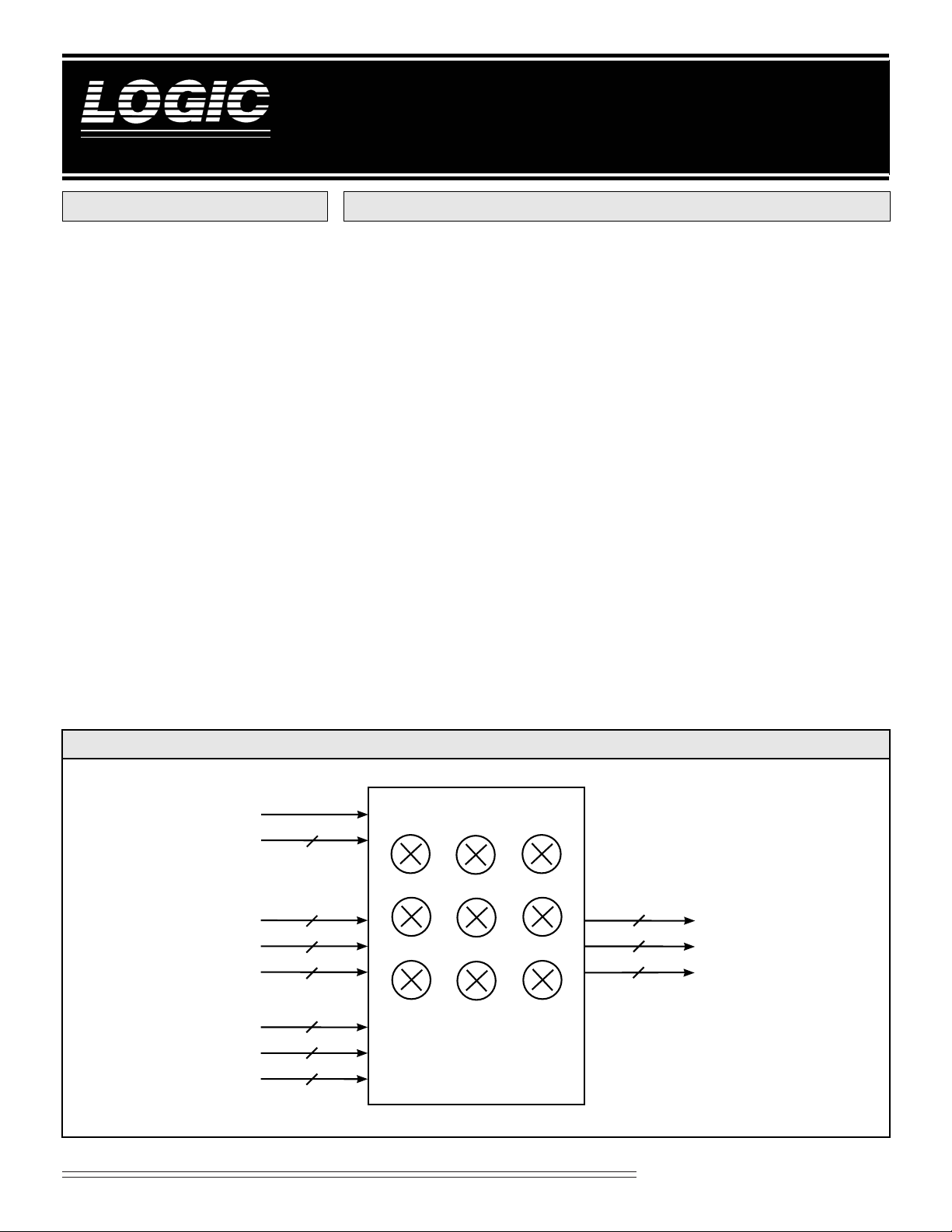
DETAILS OF OPERATION
All three input ports (A, B, C) and all
three output ports (X, Y, Z) are
utilized to implement a 3 x 3 matrix
multiplication (triple dot product).
Each truncated 12-bit output is the
sum of all three input words multiplied by the appropriate coefficients
(Table 1). The pipeline latency is five
clock cycles. Therefore, the sum of
LF2272 BLOCK DIAGRAM
CLK
1-0
CWEL
A
11-0
DATA
INPUTS
COEFFICIENT
INPUTS
{
{
B
C
KA
KB
KC
11-0
11-0
9-0
9-0
9-0
10
10
10
12
12
12
2
12
12
12
X
Y
Z
11-0
11-0
11-0
{
DATA
OUTPUTS
9-MULTIPLIER
ARRAY
Video Imaging Products
1
08/16/2000–LDS.2272-I
Page 2
DEVICES INCORPORATED
LF2272
Colorspace Converter/
Corrector (3 x 12-bits)
products will be output five clock
cycles after the input data has been
registered. New output data is
subsequently available every clock
cycle thereafter.
DATA FORMATTING
The data input ports (A, B, C) and
data output ports (X, Y, Z) are 12-bit
integer two’s complement format.
The coefficient input ports (KA, KB,
KC) are 10-bit fractional two’s
complement format. Refer to
Figures 1a and 1b.
BIT WEIGHTING
The internal sum of products of the
LF2272 can grow to 23 bits. However,
in order to keep the output format
identical to the input format, the X, Y,
and Z outputs are rounded to 12-bit
integer words. The rounding is done
only at the final output stage to allow
accuracy, with correct rounding and
overflow, for applications requiring
less than 12-bit integer words. The
user may adjust the bit weighting by
applying an identical scaling correction factor to both the input and
output data streams.
TABLE 1. LATENCY EQUATIONS
X(n+4) = A(n)KA1(n) + B(n)KB1(n) + C(n)KC1(n)
Y(n+4) = A(n)KA2(n) + B(n)KB2(n) + C(n)KC2(n)
Z(n+4) = A(n)KA3(n) + B(n)KB3(n) + C(n)KC3(n)
DATA OVERFLOW
Because the LF2272’s matched input
and output data formats accommodate unity gain (0 dB), input conditions that could lead to numeric
overflow may exist. To ensure that no
overflow conditions occur, the user
must be aware of the maximum input
data and coefficient word sizes
allowable for each specific algorithm
being performed.
FIGURE 1A.INPUT FORMATS
Data Input
11 10 9 6 5 487 3210
1121029
–2
(Sign)
7
282
Coefficient Input
SYSTEMS SMALLER THAN 12-BITS
Using a data path less than 12-bits
requires the input data to be right
justified and sign extended to 12-bits
because the LF2272 carries out all
calculations to full precision. Since all
least-significant bits are used, the
desired X, Y, and Z outputs are
rounded correctly and upper-order
output bits are used for overflow.
26252
4
2322212
0
987 43265 10
02–12–2
–2
(Sign)
20 19 18 3 2 117 0
1121029
–2
(Sign)
FIGURE 1B.OUTPUT FORMAT
11 10 9 6 5 487 3210
1121029
–2
(Sign)
2
282
–4
2–32
2–52–62
Internal Sum
8
2
2–62–72
Result
7
26252
Video Imaging Products
–7
2–82
–8
2
4
2322212
–9
–9
0
08/16/2000–LDS.2272-I
Page 3
DEVICES INCORPORATED
LF2272
Colorspace Converter/
Corrector (3 x 12-bits)
SIGNAL DEFINITIONS
Power
VCC and GND
+5 V power supply. All pins must be
connected.
Clock
CLK — Master Clock
The rising edge of CLK strobes all
enabled registers. All timing specifications are referenced to the rising
edge of CLK.
Inputs
A11-0, B11-0, C11-0 — Data Inputs
A, B, and C are the 12-bit registered
data input ports. Data presented to
these ports is latched into the multiplier input registers.
TABLE 2. COEFFICIENT INPUTS
INPUT PORT REG. AVAILABLE
KA KA1, KA2, KA3
KB KB1, KB2, KB3
KC KC1, KC2, KC3
Outputs
X11-0, Y11-0, Z11-0 — Data Outputs
X, Y, and Z are the 12-bit registered
data output ports.
Controls
CWEL1-0 — Coefficient Write Enable
The registered coefficient write enable
inputs determine which internal
coefficient register set to update
(Table 3) on the next clock cycle.
TABLE 3. COEFF. REG. UPDATE
CWEL1-0 COEFFICIENT SET
00 Hold All Registers
01 KA1, KB1, KC1
10 KA2, KB2, KC2
11 KA3, KB3, KC3
KA9-0, KB9-0, KC9-0 — Coefficient Inputs
KA, KB, and KC are the 10-bit registered coefficient input ports. Data
presented to these ports is latched into
the corresponding internal coefficient
register set defined by CWEL1-0
(Table 3) on the next rising edge of
CLK. Table 2 shows which coefficient
registers are available for each coefficient input port.
Video Imaging Products
3
08/16/2000–LDS.2272-I
Page 4

DEVICES INCORPORATED
FIGURE 2. DETAILED FUNCTIONAL DIAGRAM
12
A
KA1 KA2 KA3
10
KA
12
B
LF2272
Colorspace Converter/
Corrector (3 x 12-bits)
21 21 21
KB
KC
CWEL
KB3KB2KB1
10
21 21 21
12
C
KC1 KC2 KC3
10
21 21 21
2
12 (MSB) 12 (MSB) 12 (MSB)
XYZ
Video Imaging Products
4
08/16/2000–LDS.2272-I
Page 5

DEVICES INCORPORATED
LF2272
Colorspace Converter/
Corrector (3 x 12-bits)
MAXIMUM RATINGS
Storage temperature ........................................................................................................... –65°C to +150°C
Operating ambient temperature........................................................................................... –55°C to +125°C
VCC supply voltage with respect to ground............................................................................ –0.5 V to +7.0V
Input signal with respect to ground ............................................................................... –0.5V to VCC + 0.5 V
Signal applied to high impedance output ...................................................................... –0.5 V to VCC + 0.5 V
Output current into low outputs............................................................................................................. 25 mA
Latchup current ............................................................................................................................... > 400 mA
OPERATING CONDITIONS
Active Operation, Commercial 0°C to +70°C 4.75 V ≤ VCC ≤ 5.25 V
Active Operation, Military –55°C to +125°C 4.50 V ≤ VCC ≤ 5.50 V
ELECTRICAL CHARACTERISTICS
Above which useful life may be impaired (Notes 1, 2, 3, 8)
To meet specified electrical and switching characteristics
Mode Temperature Range (Ambient) Supply Voltage
Over Operating Conditions (Note 4)
Symbol Parameter Test Condition Min Typ Max Unit
VOH Output High Voltage Vcc = Min., IOH = –2.0 mA 2.4 V
VOL Output Low Voltage Vcc = Min., IOL = 4.0 mA 0.4 V
VIH Input High Voltage 2.0 VCC V
VIL Input Low Voltage (Note 3) 0.0 0.8 V
IIX Input Current Ground ≤ VIN ≤ VCC (Note 12) ±10 µA
IOZ Output Leakage Current (Note 12) ±40 µA
ICC1 VCC Current, Dynamic (Notes 5, 6) 160 mA
ICC2 VCC Current, Quiescent (Note 7) 12 mA
CIN Input Capacitance TA = 25°C, f = 1 MHz 10 pF
COUT Output Capacitance TA = 25°C, f = 1 MHz 10 pF
Video Imaging Products
5
08/16/2000–LDS.2272-I
Page 6

DEVICES INCORPORATED
1234567890123456789012345678901212
1
2
1
2
1
2
1
2
1
2
1
2
1
2
1
2
1
2
1
2
1
2
1
2
1
2
1
2
1
2
1
2
1
2
1
2
1
2
1
2
1
2
1
2
1
2
1234567890123456789012345678901212
8
8
8
8
8
8
8
8
8
8
8
8
8
8
8
8
8
8
8
8
8
8
8
4
SWITCHING CHARACTERISTICS
LF2272
Colorspace Converter/
Corrector (3 x 12-bits)
COMMERCIAL OPERATING RANGE (0°C to +70°C)
Notes 9, 10 (ns)
LF2272–
2345678901234567
2345678901234567
2345678901234567
Symbol Parameter Min Max Min Max Min Max
tCYC Cycle Time 33 25 20
tPWL Clock Pulse Width Low 15 10 6
tPWH Clock Pulse Width High 10 10 8
tS Input Setup Time 8 6 6
tH Input Hold Time 0 0 0
tD Output Delay 18 16 15
MILITARY OPERATING RANGE (–55°C to +125°C)
2345678901234567
2345678901234567
2345678901234567
2345678901234567
2345678901234567
2345678901234567
2345678901234567
2345678901234567
2345678901234567
2345678901234567
2345678901234567
2345678901234567
2345678901234567
2345678901234567
2345678901234567
2345678901234567
2345678901234567
2345678901234567
2345678901234567
2345678901234567
Notes 9, 10 (ns)
Symbol Parameter Min Max Min Max
tCYC Cycle Time 33 25
tPWL Clock Pulse Width Low 15 10
tPWH Clock Pulse Width High 10 10
tS Input Setup Time 12 9
tH Input Hold Time 0 0
tD Output Delay 25 20
33
*
23456789012345678901234567890121
23456789012345678901234567890121
23456789012345678901234567890121
23456789012345678901234567890121
23456789012345678901234567890121
23456789012345678901234567890121
23456789012345678901234567890121
23456789012345678901234567890121
23456789012345678901234567890121
23456789012345678901234567890121
23456789012345678901234567890121
23456789012345678901234567890121
23456789012345678901234567890121
23456789012345678901234567890121
23456789012345678901234567890121
23456789012345678901234567890121
23456789012345678901234567890121
23456789012345678901234567890121
23456789012345678901234567890121
23456789012345678901234567890121
23456789012345678901234567890121
23456789012345678901234567890121
23456789012345678901234567890121
25 20
LF2272–
*
33
25
*
SWITCHING WAVEFORM
1234 678
CLK
t
S
1-0
CWEL
KA, KB, KC
A, B, C
X
11-0
Y
11-0
Z
11-0
2345678901234567890123
*DISCONTINUED SPEED GRADE
01
t
H
Kx1 Kx2 Kx3
001.0000
t
t
PWH
PWL
10 11 00
6
5
t
D
KA1 + KB1 + KC1
KA2 + KB2 + KC2
KA3 + KB3 + KC3
Video Imaging Products
08/16/2000–LDS.2272-I
Page 7

DEVICES INCORPORATED
OE
0.2 V
t
DIS
t
ENA
0.2 V
1.5 V 1.5 V
3.0V Vth
1
Z
0
Z
Z
1
Z
0
1.5 V
1.5 V
0V Vth
VOL*
V
OH
*
V
OL
*
V
OH
*
Measured V
OL
with IOH = –10mA and IOL = 10mA
Measured V
OH
with IOH = –10mA and IOL = 10mA
S1
I
OH
I
OL
V
TH
C
L
DUT
NOTES
LF2272
Colorspace Converter/
Corrector (3 x 12-bits)
1. Maximum Ratings indicate stress
specifications only. Functional operation of these products at values beyond
those indicated in the Operating Conditions table is not implied. Exposure to
maximum rating conditions for extended periods may affect reliability.
2. The products described by this specification include internal circuitry designed to protect the chip from damaging substrate injection currents and accumulations of static charge. Nevertheless, conventional precautions should
be observed during storage, handling,
and use of these circuits in order to
avoid exposure to excessive electrical
stress values.
3. This device provides hard clamping of
transient undershoot and overshoot. Input levels below ground or above VCC
will be clamped beginning at –0.6 V and
VCC + 0.6 V. The device can withstand
indefinite operation with inputs in the
range of –0.5 V to +7.0 V. Device operation will not be adversely affected, however, input current levels will be well in
excess of 100 mA.
9. AC specifications are tested with
input transition times less than 3 ns,
output reference levels of 1.5 V (except
tDIS test), and input levels of nominally
0 to 3.0 V. Output loading may be a
resistive divider which provides for
specified IOH and IOL at an output
voltage of VOH min and VOL max
respectively. Alternatively, a diode
bridge with upper and lower current
sources of IOH and IOL respectively,
and a balancing voltage of 1.5 V may be
used. Parasitic capacitance is 30 pF
minimum, and may be distributed.
This device has high-speed outputs capable of large instantaneous current
pulses and fast turn-on/turn-off times.
As a result, care must be exercised in the
testing of this device. The following
measures are recommended:
a. A 0.1 µF ceramic capacitor should be
installed between VCC and Ground
leads as close to the Device Under Test
(DUT) as possible. Similar capacitors
should be installed between device VCC
and the tester common, and device
ground and tester common.
11. For the tENA test, the transition is
measured to the 1.5 V crossing point
with datasheet loads. For the tDIS test,
the transition is measured to the
±200mV level from the measured
steady-state output voltage with
±10mA loads. The balancing voltage, VTH, is set at 3.5 V for Z-to-0
and 0-to-Z tests, and set at 0 V for Zto-1 and 1-to-Z tests.
12. These parameters are only tested at
the high temperature extreme, which is
the worst case for leakage current.
FIGURE A. OUTPUT LOADING CIRCUIT
FIGURE B. THRESHOLD LEVELS
4. Actual test conditions may vary from
those designated but operation is guaranteed as specified.
5. Supply current for a given application can be accurately approximated by:
2
NCV F
where
4
N = total number of device outputs
C = capacitive load per output
V = supply voltage
F = clock frequency
6. Tested with all outputs changing every cycle and no load, at a 20 MHz clock
rate.
7. Tested with all inputs within 0.1 V of
VCC or Ground, no load.
8. These parameters are guaranteed
but not 100% tested.
b. Ground and VCC supply planes
must be brought directly to the DUT
socket or contactor fingers.
c. Input voltages should be adjusted to
compensate for inductive ground and VCC
noise to maintain required DUT input
levels relative to the DUT ground pin.
10. Each parameter is shown as a minimum or maximum value. Input requirements are specified from the point
of view of the external system driving
the chip. Setup time, for example, is
specified as a minimum since the external system must supply at least that
much time to meet the worst-case requirements of all parts. Responses from
the internal circuitry are specified from
the point of view of the device. Output
delay, for example, is specified as a
maximum since worst-case operation of
any device always provides data within
that time.
7
Video Imaging Products
08/16/2000–LDS.2272-I
Page 8

DEVICES INCORPORATED
ORDERING INFORMATION
LF2272
Colorspace Converter/
Corrector (3 x 12-bits)
120-pin
GND
Y
Y
V
GND
V
GND
X7X8VCCX9X10X11GND
120
119
118
X
6
1
X
5
2
X
4
3
X
3
4
X
2
5
X
1
6
X
0
7
8
11
9
10
10
Y
9
11
CC
12
Y
8
13
Y
7
14
Y
6
15
16
Y
5
17
Y
4
18
Y
0
19
CC
20
Y
1
21
Y
2
22
Y
3
23
24
0
Z
25
Z
1
26
Z
2
27
Z
3
28
Z
4
29
Z
5
30
117
3132333435363738394041424344454647484950515253545556575859
116
115
114
GND
113
GND
112
C11C10C9C8C7GND
111
110
109
108
107
106
Top
View
C6C5C4VCCC3C2C1C0B11B10B9B8B7B6B
105
104
103
999897969594939291
102
101
100
5
90
B
4
B
89
88
87
86
85
84
83
82
81
80
79
78
77
76
75
74
73
72
71
70
69
68
67
66
65
64
63
62
61
60
3
CLK
2
B
B
1
B
0
A
11
A
10
A
9
A
8
A
7
A
6
A
5
A
4
A
3
A
2
A
1
A
0
GND
CWE
CWE
KA
KA
KA
KA
KA
KA
KA
KA
KA
0
1
9
8
7
6
5
4
3
2
1
Speed
25 ns
20 ns
8
9
GND
Z
Z10Z
Z6Z7Z
0°C to +70°C — COMMERCIAL SCREENING
–40°C to +85°C — COMMERCIAL SCREENING
3
11
KC0KC1KC2KC
GND
4KC5KC6
KC
Plastic Quad Flatpack
(Q1)
LF2272QC25
LF2272QC20
9KB0KB1KB2KB3KB4KB5KB6KB7KB8KB9KA0
CC
KC7KC8KC
V
Video Imaging Products
8
08/16/2000–LDS.2272-I
Page 9

DEVICES INCORPORATED
1
1
1
1
1
1
1
1
1
1
1
1
1
1
1
1
1
1
1
1
1
1
1
1
1
1
1
1
1
1
1
1
1
1
1
1
1
1
1
1
1
1
1
1
1
1
1
1
1
1
1
1
1
1
1
1
1
1
1
1
1
1
1
1
1
1
1
Colorspace Converter/
Corrector (3 x 12-bits)
ORDERING INFORMATION
23456789012345678901234567890121234567890123456789012345678901212345678901234567890123456789012
23456789012345678901234567890121234567890123456789012345678901212345678901234567890123456789012
23456789012345678901234567890121234567890123456789012345678901212345678901234567890123456789012
23456789012345678901234567890121234567890123456789012345678901212345678901234567890123456789012
120-pin
23456789012345678901234567890121234567890123456789012345678901212345678901234567890123456789012
23456789012345678901234567890121234567890123456789012345678901212345678901234567890123456789012
23456789012345678901234567890121234567890123456789012345678901212345678901234567890123456789012
23456789012345678901234567890121234567890123456789012345678901212345678901234567890123456789012
23456789012345678901234567890121234567890123456789012345678901212345678901234567890123456789012
23456789012345678901234567890121234567890123456789012345678901212345678901234567890123456789012
23456789012345678901234567890121234567890123456789012345678901212345678901234567890123456789012
23456789012345678901234567890121234567890123456789012345678901212345678901234567890123456789012
23456789012345678901234567890121234567890123456789012345678901212345678901234567890123456789012
23456789012345678901234567890121234567890123456789012345678901212345678901234567890123456789012
23456789012345678901234567890121234567890123456789012345678901212345678901234567890123456789012
23456789012345678901234567890121234567890123456789012345678901212345678901234567890123456789012
23456789012345678901234567890121234567890123456789012345678901212345678901234567890123456789012
23456789012345678901234567890121234567890123456789012345678901212345678901234567890123456789012
23456789012345678901234567890121234567890123456789012345678901212345678901234567890123456789012
23456789012345678901234567890121234567890123456789012345678901212345678901234567890123456789012
23456789012345678901234567890121234567890123456789012345678901212345678901234567890123456789012
23456789012345678901234567890121234567890123456789012345678901212345678901234567890123456789012
23456789012345678901234567890121234567890123456789012345678901212345678901234567890123456789012
23456789012345678901234567890121234567890123456789012345678901212345678901234567890123456789012
23456789012345678901234567890121234567890123456789012345678901212345678901234567890123456789012
23456789012345678901234567890121234567890123456789012345678901212345678901234567890123456789012
23456789012345678901234567890121234567890123456789012345678901212345678901234567890123456789012
23456789012345678901234567890121234567890123456789012345678901212345678901234567890123456789012
23456789012345678901234567890121234567890123456789012345678901212345678901234567890123456789012
23456789012345678901234567890121234567890123456789012345678901212345678901234567890123456789012
23456789012345678901234567890121234567890123456789012345678901212345678901234567890123456789012
23456789012345678901234567890121234567890123456789012345678901212345678901234567890123456789012
23456789012345678901234567890121234567890123456789012345678901212345678901234567890123456789012
23456789012345678901234567890121234567890123456789012345678901212345678901234567890123456789012
23456789012345678901234567890121234567890123456789012345678901212345678901234567890123456789012
23456789012345678901234567890121234567890123456789012345678901212345678901234567890123456789012
23456789012345678901234567890121234567890123456789012345678901212345678901234567890123456789012
23456789012345678901234567890121234567890123456789012345678901212345678901234567890123456789012
23456789012345678901234567890121234567890123456789012345678901212345678901234567890123456789012
23456789012345678901234567890121234567890123456789012345678901212345678901234567890123456789012
23456789012345678901234567890121234567890123456789012345678901212345678901234567890123456789012
23456789012345678901234567890121234567890123456789012345678901212345678901234567890123456789012
23456789012345678901234567890121234567890123456789012345678901212345678901234567890123456789012
23456789012345678901234567890121234567890123456789012345678901212345678901234567890123456789012
23456789012345678901234567890121234567890123456789012345678901212345678901234567890123456789012
23456789012345678901234567890121234567890123456789012345678901212345678901234567890123456789012
23456789012345678901234567890121234567890123456789012345678901212345678901234567890123456789012
23456789012345678901234567890121234567890123456789012345678901212345678901234567890123456789012
23456789012345678901234567890121234567890123456789012345678901212345678901234567890123456789012
23456789012345678901234567890121234567890123456789012345678901212345678901234567890123456789012
23456789012345678901234567890121234567890123456789012345678901212345678901234567890123456789012
23456789012345678901234567890121234567890123456789012345678901212345678901234567890123456789012
23456789012345678901234567890121234567890123456789012345678901212345678901234567890123456789012
23456789012345678901234567890121234567890123456789012345678901212345678901234567890123456789012
23456789012345678901234567890121234567890123456789012345678901212345678901234567890123456789012
23456789012345678901234567890121234567890123456789012345678901212345678901234567890123456789012
23456789012345678901234567890121234567890123456789012345678901212345678901234567890123456789012
23456789012345678901234567890121234567890123456789012345678901212345678901234567890123456789012
23456789012345678901234567890121234567890123456789012345678901212345678901234567890123456789012
23456789012345678901234567890121234567890123456789012345678901212345678901234567890123456789012
23456789012345678901234567890121234567890123456789012345678901212345678901234567890123456789012
23456789012345678901234567890121234567890123456789012345678901212345678901234567890123456789012
23456789012345678901234567890121234567890123456789012345678901212345678901234567890123456789012
23456789012345678901234567890121234567890123456789012345678901212345678901234567890123456789012
23456789012345678901234567890121234567890123456789012345678901212345678901234567890123456789012
23456789012345678901234567890121234567890123456789012345678901212345678901234567890123456789012
23456789012345678901234567890121234567890123456789012345678901212345678901234567890123456789012
Speed
0°C to +70°C — COMMERCIAL SCREENING
–55°C to +125°C — COMMERCIAL SCREENING
–55°C to +125°C — MIL-STD-883 COMPLIANT
12345
A
X
9
X
7
X
B
X
5
X
4
X
C
X
2
X
1
X
D
X
0
Y
11
X
E
Y
10
Y
9
GND
F
Y
8
Y
7
V
G
Y
6
Y
5
GND
H
V
Y
0
Y
4
J
Y
2
Y
1
GND
K
Z
Z
0
Y
3
L
Z
4
Z
1
Z
M
Z
7
Z
2
Z
N
Z
8
Z
5
Z
6
GND
C
11
C
8
C
9
C
10
KEY
Top View
GND
CC
10
X
11
8
6
GND
V
CC
GND
3
Through Package
(i.e., Component Side Pinout)
CC
3
GND
6
Z
9
KC
10
0
GND
KC
KC
KC
KC
2
4
3
KC
5
11
1
Discontinued Package
Ceramic Pin Grid Array
(G4)
9
7 8 9 10 11
C
7
C
5
C
3
C
1
C
6
C
4
C
2
B
11
V
CC
C
0
B
8
CC
KB
0
KB
V
KC
KC
6
KC
7
KC
4
KB
8
9
KB
2
KB
5
8
KB
1
KB
3
12 13
B
10
B
7
B
4
B
9
B
6
B
2
B
5
B
3
B
1
CLK
B
0
A
10
11
A
9
A
KA
KA
KA
KB
8
A
6
A
5
A
2
A
4
A
0
A
1
1
CWEL
0
7
KA
9
5
KA
6
2
KA
3
7
KA
0
A
A
7
A
3
GND
KA
8
CWEL
KA
4
KA
1
KB
9
KB
6
Video Imaging Products
LF2272
08/16/2000–LDS.2272-I
 Loading...