

Page 1
DEVICES INCORPORATED
LF2246
11 x 10-bit Image Filter
LF2246
DEVICES INCORPORATED
FEATURES DESCRIPTION
❑❑
❑ 66 MHz Data and Coefficient Input
❑❑
and Computation Rate
❑❑
❑ Four 11 x 10-bit Multipliers with
❑❑
Individual Data and Coefficient
Inputs and a 25-bit Accumulator
❑❑
❑ User-Selectable Fractional or
❑❑
Integer Two’s Complement Data
Formats
❑❑
❑ Fully Registered, Pipelined Archi-
❑❑
tecture
❑❑
❑ Input and Output Data Registers,
❑❑
with User-Configurable Enables
❑❑
❑ Three-State Outputs
❑❑
❑❑
❑ Fully TTL Compatible
❑❑
❑❑
❑ Ideally Suited for Image Processing
❑❑
and Filtering Applications
❑❑
❑ Replaces TRW/Raytheon/Fairchild
❑❑
TMC2246
❑❑
❑ 120-pin PQFPP
❑❑
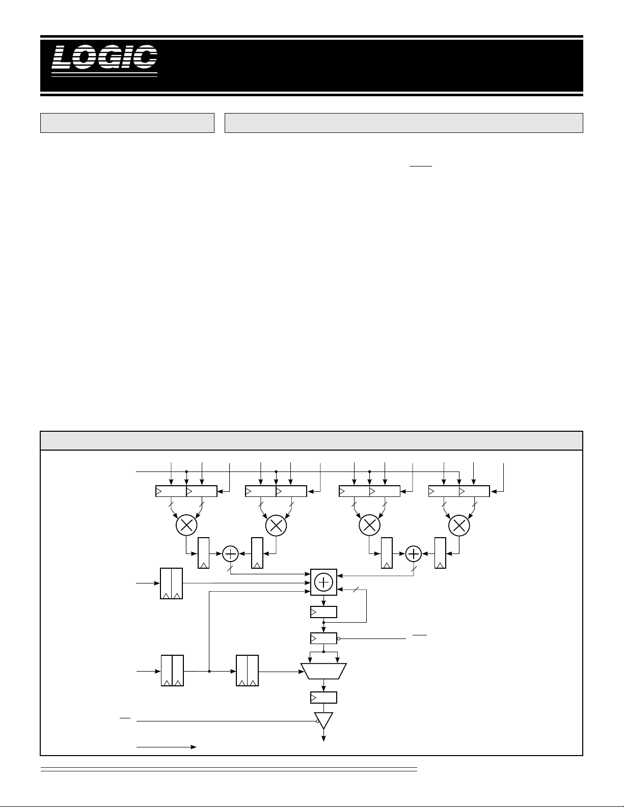
The LF2246 consists of an array of
four 11 x 10-bit registered multipliers
followed by a summer and a 25-bit
accumulator. All multiplier inputs
are user accessible and can be updated every clock cycle with either
fractional or integer two’s complement data. The pipelined architecture
has fully registered input and output
ports and an asynchronous three-state
output enable control to simplify the
design of complex systems. The
pipeline latency for all inputs is five
clock cycles.
Storage for mixing and filtering
coefficients can be accomplished by
holding the data or coefficient inputs
over multiple clock cycles. A 25-bit
accumulator path allows cumulative
word growth which may be internally
rounded to 16 bits. Output data is
updated every clock cycle and may be
held under user control. All inputs,
11 x 10-bit Image Filter
outputs, and controls are registered
on the rising edge of clock, except for
OEN. The LF2246 operates at a clock
rate of 66 MHz over the full temperature and supply voltage ranges.
The LF2246 is applicable for performing pixel interpolation in image
manipulation and filtering applications. The LF2246 can perform a
bilinear interpolation of an image (4pixel kernels) at real-time video rates
when used with an image resampling
sequencer. Larger kernels or more
complex functions can be realized by
utilizing multiple devices.
Unrestricted access to all data and
coefficient input ports provides the
LF2246 with considerable flexibility in
applications such as digital filters,
adaptive FIR filters, mixers, and other
similar systems requiring high-speed
processing.
LF2246 BLOCK DIAGRAM
D1
ENSEL
10
ACC
FSEL
OEN
9–0
C1
10–0
ENB1 D2
11 10 11 10 11 10 11
22
9–0
C2
10–0
ENB2
MS LS
D3
9–0
C3
10–0
ENB3 D4
25
OCEN
22
9–0C410–0
ENB4
CLK
TO ALL REGISTERS
2-11
S
15–0
Video Imaging Products
08/16/2000–LDS.2246-K
Page 2
DEVICES INCORPORATED
LF2246
11 x 10-bit Image Filter
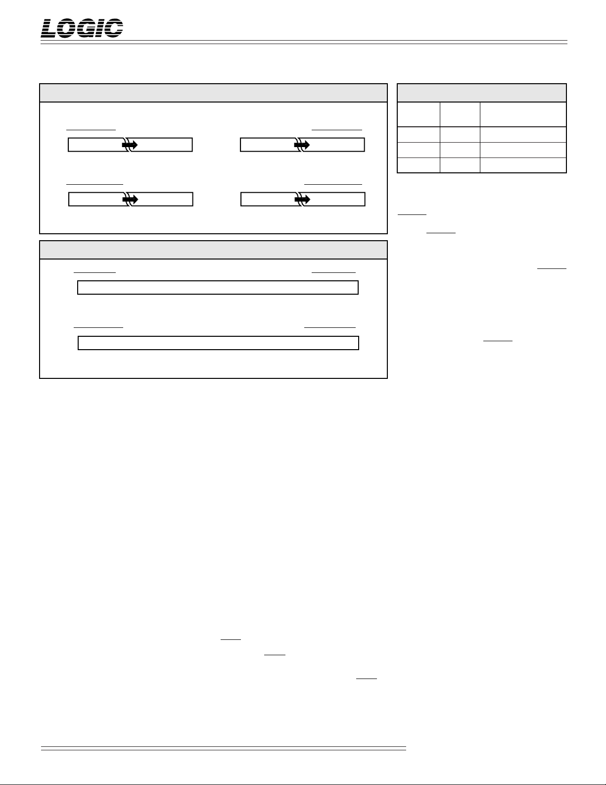
FIGURE 1A.INPUT FORMATS
Data
Fractional Two’s Complement (FSEL = 0)
987 210
–2
(Sign)
0
2–12
–2
2–72–82
–9
Integer Two’s Complement (FSEL = 1)
987 210
–2
(Sign)
9
282
7
22212
0
FIGURE 1B.OUTPUT FORMATS
Fractional Two’s Complement (FSEL = 0)
15 14 13 10 9 81211 76543210
6
–2
(Sign)
15 14 13 10 9 81211 76543210
15
–2
(Sign)
SIGNAL DEFINITIONS
Power
VCC and GND
+5 V power supply. All pins must be
connected.
Clock
CLK — Master Clock
The rising edge of CLK strobes all enabled registers. All timing specifications are referenced to the rising edge of
CLK.
Inputs
D19–0–D49–0 — Data Input
D1–D4 are 10-bit data input registers.
The LSB is DN0 (Figure 1a).
C110–0–C410–0 — Coefficient Input
C1–C4 are 11-bit coefficient input registers. The LSB is CN0 (Figure 1a).
Outputs
S15–0 — Data Output
The current 16-bit result is available on
the S15–0 outputs (Figure 1b).
252
4
232
2
21202
Integer Two’s Complement (FSEL = 1)
2142
13
2122
11
210292
Coefficient
10 9 8 2 1 0
–2
(Sign)
1
202
–1
2–72–82
–9
10 9 8 2 1 0
10
–2
(Sign)
–1
2–22–32–42–52–62–72–82
8
272625242322212
292
8
22212
0
–9
0
Controls
ENB1–ENB4 — Input Enable
The ENBN (N = 1, 2, 3, or 4) input allows
either or both the DN and CN registers to
be updated on each clock cycle. When
ENBN is LOW, registers DN and CN are
both strobed by the next rising edge of
CLK. When ENBN is HIGH and ENSEL
is LOW, register DN is strobed while
register CN is held. If both ENBN and
ENSEL are HIGH, register DN is held,
and register CN is strobed (Table 1).
ENSEL — Enable Select
The ENSEL input in conjunction with
the individual input enables ENB1–
ENB4 determines whether the data or
the coefficient input registers will be
held on the next rising edge of CLK
(Table 1).
OEN — Output Enable
When the OEN signal is LOW, the current data in the output register is available on the S15–0 pins. When OEN is
HIGH, the outputs are in a high-impedance state.
TABLE 1. INPUT REGISTER CONTROL
INPUT REGISTER
ENB1-4 ENSEL HELD
1 1 Data ‘N’
1 0 Coefficient ‘N’
0 X None
X = “Don’t Care”
‘N’ = 1, 2, 3, or 4
OCEN — Clock Enable
When OCEN is LOW, data in the premux register (accumulator output) is
loaded into the output register on the
next rising edge of CLK. When OCEN
is HIGH, data in the pre-mux register is
held preventing the output register’s
contents from changing (if FSEL does
not change). Accumulation continues
internally as long as ACC is HIGH,
despite the state of OCEN.
FSEL — Format Select
When the FSEL input is LOW, the data
input during the current clock cycle is
assumed to be in fractional two’s
complement format, and the upper 16
bits of the accumulator are presented at
the output. Rounding of the accumulator result to 16 bits is performed if the
accumulator control input ACC is
LOW. When FSEL is HIGH, the data
input is assumed to be in integer two’s
complement format, and the lower 16
bits of the accumulator are presented at
the output. No rounding is performed
when FSEL is HIGH.
ACC — Accumulator Control
The ACC input determines whether internal accumulation is performed on
the data input during the current clock
cycle. If ACC is LOW, no accumulation
is performed, the prior accumulated
sum is cleared, and the current sum of
products is output. If FSEL is also LOW,
one-half LSB rounding to 16 bits is performed on the result. This allows summations without propagating roundoff
errors. When ACC is HIGH, the emerging product is added to the sum of the
previous products, without additional
rounding.
2-12
Video Imaging Products
08/16/2000–LDS.2246-K
Page 3
DEVICES INCORPORATED
LF2246
11 x 10-bit Image Filter
MAXIMUM RATINGS
Storage temperature ........................................................................................................... –65°C to +150°C
Operating ambient temperature........................................................................................... –55°C to +125°C
VCC supply voltage with respect to ground............................................................................ –0.5 V to +7.0V
Input signal with respect to ground ............................................................................... –0.5 V to VCC + 0.5 V
Signal applied to high impedance output ...................................................................... –0.5 V to VCC + 0.5 V
Output current into low outputs............................................................................................................. 25 mA
Latchup current ................................................................................................................ ............... > 400 mA
OPERATING CONDITIONS
Active Operation, Commercial 0°C to +70°C 4.75 V ≤ VCC ≤ 5.25 V
Active Operation, Military –55°C to +125°C 4.50 V ≤ VCC ≤ 5.50 V
ELECTRICAL CHARACTERISTICS
Above which useful life may be impaired (Notes 1, 2, 3, 8)
To meet specified electrical and switching characteristics
Mode Temperature Range (Ambient) Supply Voltage
Over Operating Conditions (Note 4)
Symbol Parameter Test Condition Min Typ Max Unit
VOH Output High Voltage VCC = Min., IOH = –2.0 mA 2.4 V
VOL Output Low Voltage VCC = Min., IOL = 4.0 mA 0.4 V
VIH Input High Voltage 2.0 VCC V
V IL Input Low Voltage (Note 3) 0.0 0.8 V
IIX Input Current Ground ≤ VIN ≤ VCC (Note 12) ±10 µA
IOZ Output Leakage Current (Note 12) ±40 µA
ICC1 VCC Current, Dynamic (Notes 5, 6) 100 mA
ICC2 VCC Current, Quiescent (Note 7) 6mA
CIN Input Capacitance TA = 25°C, f = 1 MHz 10 pF
COUT Output Capacitance TA = 25°C, f = 1 MHz 10 pF
2-13
Video Imaging Products
08/16/2000–LDS.2246-K
Page 4

DEVICES INCORPORATED
7
7
7
7
7
7
7
7
7
7
7
7
7
7
7
7
7
7
7
7
7
7
7
7
7
7
7
7
7
7
7
7
7
7
7
7
7
7
7
7
7
7
7
7
7
7
7
7
123456789012345678901234
4
4
4
4
4
4
4
4
4
4
4
4
4
4
4
4
4
4
4
4
4
4
4
4
4
4
4
4
4
4
4
4
4
4
4
4
4
4
4
4
4
4
4
4
4
4
4
123456789012345678901234
4
SWITCHING CHARACTERISTICS
LF2246
11 x 10-bit Image Filter
COMMERCIAL OPERATING RANGE (0°C to +70°C)
Symbol Parameter Min Max Min Max Min Max
tCYC Cycle Time 33 25 15
tPWL Clock Pulse Width Low 15 10 7
tPWH Clock Pulse Width High 10 10 7
tS Input Setup Time 10 8 5
tH Input Hold Time 0 0 0
tD Output Delay 15 13 11
tDIS Three-State Output Disable Delay (Note 11) 15 15 15
tENA Three-State Output Enable Delay (Note 11) 15 15 15
MILITARY OPERATING RANGE (–55°C to +125°C)
Symbol Parameter Min Max Min Max
tCYC Cycle Time 33 25
tPWL Clock Pulse Width Low 15 10
tPWH Clock Pulse Width High 10 10
tS Input Setup Time 10 8
tH Input Hold Time 0 0
tD Output Delay 15 13
tDIS Three-State Output Disable Delay (Note 11) 15 15
tENA Three-State Output Enable Delay (Note 11) 15 15
Notes 9, 10 (ns)
12345678901234567890123
12345678901234567890123
12345678901234567890123
12345678901234567890123
12345678901234567890123
12345678901234567890123
12345678901234567890123
12345678901234567890123
12345678901234567890123
12345678901234567890123
12345678901234567890123
12345678901234567890123
12345678901234567890123
12345678901234567890123
12345678901234567890123
12345678901234567890123
12345678901234567890123
12345678901234567890123
12345678901234567890123
12345678901234567890123
12345678901234567890123
12345678901234567890123
12345678901234567890123
12345678901234567890123
12345678901234567890123
12345678901234567890123
12345678901234567890123
12345678901234567890123
12345678901234567890123
12345678901234567890123
12345678901234567890123
12345678901234567890123
12345678901234567890123
12345678901234567890123
12345678901234567890123
12345678901234567890123
12345678901234567890123
12345678901234567890123
12345678901234567890123
12345678901234567890123
12345678901234567890123
12345678901234567890123
12345678901234567890123
12345678901234567890123
12345678901234567890123
12345678901234567890123
12345678901234567890123
Notes 9, 10 (ns)
33
LF2246–
*
23456789012345678901234567890121234567890123456
23456789012345678901234567890121234567890123456
23456789012345678901234567890121234567890123456
23456789012345678901234567890121234567890123456
23456789012345678901234567890121234567890123456
23456789012345678901234567890121234567890123456
23456789012345678901234567890121234567890123456
23456789012345678901234567890121234567890123456
23456789012345678901234567890121234567890123456
23456789012345678901234567890121234567890123456
23456789012345678901234567890121234567890123456
23456789012345678901234567890121234567890123456
23456789012345678901234567890121234567890123456
23456789012345678901234567890121234567890123456
23456789012345678901234567890121234567890123456
23456789012345678901234567890121234567890123456
23456789012345678901234567890121234567890123456
23456789012345678901234567890121234567890123456
23456789012345678901234567890121234567890123456
23456789012345678901234567890121234567890123456
23456789012345678901234567890121234567890123456
23456789012345678901234567890121234567890123456
23456789012345678901234567890121234567890123456
23456789012345678901234567890121234567890123456
23456789012345678901234567890121234567890123456
23456789012345678901234567890121234567890123456
23456789012345678901234567890121234567890123456
23456789012345678901234567890121234567890123456
23456789012345678901234567890121234567890123456
23456789012345678901234567890121234567890123456
23456789012345678901234567890121234567890123456
23456789012345678901234567890121234567890123456
23456789012345678901234567890121234567890123456
23456789012345678901234567890121234567890123456
23456789012345678901234567890121234567890123456
23456789012345678901234567890121234567890123456
23456789012345678901234567890121234567890123456
23456789012345678901234567890121234567890123456
23456789012345678901234567890121234567890123456
23456789012345678901234567890121234567890123456
23456789012345678901234567890121234567890123456
23456789012345678901234567890121234567890123456
23456789012345678901234567890121234567890123456
23456789012345678901234567890121234567890123456
23456789012345678901234567890121234567890123456
23456789012345678901234567890121234567890123456
23456789012345678901234567890121234567890123456
23456789012345678901234567890121234567890123456
25 15
LF2246–
*
33
25
*
SWITCHING WAVEFORMS
D1
9-0
C1
10-0
CONTROLS
(Except OEN)
2345678901234567890123
*DISCONTINUED SPEED GRADE
– D4
– C4
CLK
10-0
OEN
15-0
S
123456
t
H
t
9-0
D
N
t
S
C
N
D
N+1
C
N+1
t
DIS
PWH
HIGH IMPEDANCE
2-14
t
ENA
t
PWL
t
D
S
N–1
S
N
S
N+1
Video Imaging Products
08/16/2000–LDS.2246-K
Page 5

DEVICES INCORPORATED
S1
I
OH
I
OL
V
TH
C
L
DUT
OE
0.2 V
t
DIS
t
ENA
0.2 V
1.5 V 1.5 V
3.5V Vth
1
Z
0
Z
Z
1
Z
0
1.5 V
1.5 V
0V Vth
VOL*
V
OH
*
V
OL
*
V
OH
*
Measured V
OL
with IOH = –10mA and IOL = 10mA
Measured V
OH
with IOH = –10mA and IOL = 10mA
NOTES
LF2246
11 x 10-bit Image Filter
1. Maximum Ratings indicate stress
specifications only. Functional operation of these products at values beyond
those indicated in the Operating Conditions table is not implied. Exposure to
maximum rating conditions for extended periods may affect reliability.
2. The products described by this specification include internal circuitry designed to protect the chip from damaging substrate injection currents and accumulations of static charge. Nevertheless, conventional precautions should
be observed during storage, handling,
and use of these circuits in order to
avoid exposure to excessive electrical
stress values.
3. This device provides hard clamping of
transient undershoot and overshoot. Input levels below ground or above VCC
will be clamped beginning at –0.6 V and
VCC + 0.6 V. The device can withstand
indefinite operation with inputs in the
range of –0.5 V to +7.0 V. Device operation will not be adversely affected, however, input current levels will be well in
excess of 100 mA.
9. AC specifications are tested with
input transition times less than 3 ns,
output reference levels of 1.5 V (except
tDIS test), and input levels of nominally
0 to 3.0 V. Output loading may be a
resistive divider which provides for
specified IOH and IOL at an output
voltage of VOH min and VOL max
respectively. Alternatively, a diode
bridge with upper and lower current
sources of IOH and IOL respectively,
and a balancing voltage of 1.5 V may be
used. Parasitic capacitance is 30 pF
minimum, and may be distributed.
This device has high-speed outputs capable of large instantaneous current
pulses and fast turn-on/turn-off times.
As a result, care must be exercised in the
testing of this device. The following
measures are recommended:
a. A 0.1 µF ceramic capacitor should be
installed between VCC and Ground
leads as close to the Device Under Test
(DUT) as possible. Similar capacitors
should be installed between device VCC
and the tester common, and device
ground and tester common.
11. For the tENA test, the transition is
measured to the 1.5 V crossing point
with datasheet loads. For the tDIS test,
the transition is measured to the
±200mV level from the measured
steady-state output voltage with
±10mA loads. The balancing voltage, VTH, is set at 3.5 V for Z-to-0
and 0-to-Z tests, and set at 0 V for Zto-1 and 1-to-Z tests.
12. These parameters are only tested at
the high temperature extreme, which is
the worst case for leakage current.
FIGURE A. OUTPUT LOADING CIRCUIT
FIGURE B. THRESHOLD LEVELS
4. Actual test conditions may vary from
those designated but operation is guaranteed as specified.
5. Supply current for a given application can be accurately approximated by:
2
NCV F
where
4
N = total number of device outputs
C = capacitive load per output
V = supply voltage
F = clock frequency
6. Tested with all outputs changing every cycle and no load, at a 30 MHz clock
rate.
7. Tested with all inputs within 0.1 V of
VCC or Ground, no load.
8. These parameters are guaranteed
but not 100% tested.
b. Ground and VCC supply planes
must be brought directly to the DUT
socket or contactor fingers.
c. Input voltages should be adjusted to
compensate for inductive ground and VCC
noise to maintain required DUT input
levels relative to the DUT ground pin.
10. Each parameter is shown as a minimum or maximum value. Input requirements are specified from the point
of view of the external system driving
the chip. Setup time, for example, is
specified as a minimum since the external system must supply at least that
much time to meet the worst-case requirements of all parts. Responses from
the internal circuitry are specified from
the point of view of the device. Output
delay, for example, is specified as a
maximum since worst-case operation of
any device always provides data within
that time.
2-15
Video Imaging Products
08/16/2000–LDS.2246-K
Page 6

DEVICES INCORPORATED
ORDERING INFORMATION
LF2246
11 x 10-bit Image Filter
120-pin
CLK
FSEL
ACC
OCEN
OEN
S
S
GND
S
S
S
V
S
GND
V
GND
D1
D1
D1
D1
ENSEL
ENB4
ENB1
ENB2
ENB3
D49D48D47D46D45D44D43D42D41GND
120
119
118
117
116
115
114
113
112
111
110
1
2
3
4
5
15
6
14
7
8
13
9
12
10
11
11
CC
12
10
13
S
9
14
S
8
15
16
7
S
17
S
6
18
S
5
19
CC
20
S
4
21
S
3
22
S
2
23
24
1
S
25
S
0
26
9
27
8
28
7
29
6
30
3132333435363738394041424344454647484950515253545556575859
109
D40C410C49VCCC48C47C46C45C44C43C42C41C40C30C3
108
107
106
105
104
103
999897969594939291
102
101
100
Top
View
1
90
C3
C3
C3
C3
C3
C3
C3
C3
C3
D3
D3
D3
D3
D3
D3
D3
D3
D3
GND
D3
D2
D2
D2
D2
D2
D2
D2
D2
D2
D2
2
3
4
5
6
7
8
9
10
0
1
2
3
4
5
6
7
8
9
9
8
7
6
5
4
3
2
1
0
89
88
87
86
85
84
83
82
81
80
79
78
77
76
75
74
73
72
71
70
69
68
67
66
65
64
63
62
61
60
Speed
25 ns
15 ns
D15D14D13D12D11D1
0
0°C to +70°C — COMMERCIAL SCREENING
–40°C to +85°C — COMMERCIAL SCREENING
6
10
C19C18C17C1
C1
GND
5C14C13
C1
Plastic Quad Flatpack
(Q1)
LF2246QC25
LF2246QC15
CC
C12C11C10C20C21C22C23C24C25C26C27C28C2
V
9
10
C2
2-16
Video Imaging Products
08/16/2000–LDS.2246-K
Page 7

DEVICES INCORPORATED
1
1
1
1
1
1
1
1
1
1
1
1
1
1
1
1
1
1
1
1
1
1
1
1
1
1
1
1
1
1
1
1
1
1
1
1
1
1
1
1
1
1
1
1
1
1
1
1
1
1
1
1
1
1
1
1
1
1
1
1
1
1
1
1
1
1
1
11 x 10-bit Image Filter
ORDERING INFORMATION
23456789012345678901234567890121234567890123456789012345678901212345678901234567890123456789012
23456789012345678901234567890121234567890123456789012345678901212345678901234567890123456789012
23456789012345678901234567890121234567890123456789012345678901212345678901234567890123456789012
120-pin
23456789012345678901234567890121234567890123456789012345678901212345678901234567890123456789012
23456789012345678901234567890121234567890123456789012345678901212345678901234567890123456789012
23456789012345678901234567890121234567890123456789012345678901212345678901234567890123456789012
23456789012345678901234567890121234567890123456789012345678901212345678901234567890123456789012
23456789012345678901234567890121234567890123456789012345678901212345678901234567890123456789012
23456789012345678901234567890121234567890123456789012345678901212345678901234567890123456789012
23456789012345678901234567890121234567890123456789012345678901212345678901234567890123456789012
23456789012345678901234567890121234567890123456789012345678901212345678901234567890123456789012
23456789012345678901234567890121234567890123456789012345678901212345678901234567890123456789012
23456789012345678901234567890121234567890123456789012345678901212345678901234567890123456789012
23456789012345678901234567890121234567890123456789012345678901212345678901234567890123456789012
23456789012345678901234567890121234567890123456789012345678901212345678901234567890123456789012
23456789012345678901234567890121234567890123456789012345678901212345678901234567890123456789012
23456789012345678901234567890121234567890123456789012345678901212345678901234567890123456789012
23456789012345678901234567890121234567890123456789012345678901212345678901234567890123456789012
23456789012345678901234567890121234567890123456789012345678901212345678901234567890123456789012
23456789012345678901234567890121234567890123456789012345678901212345678901234567890123456789012
23456789012345678901234567890121234567890123456789012345678901212345678901234567890123456789012
23456789012345678901234567890121234567890123456789012345678901212345678901234567890123456789012
23456789012345678901234567890121234567890123456789012345678901212345678901234567890123456789012
23456789012345678901234567890121234567890123456789012345678901212345678901234567890123456789012
23456789012345678901234567890121234567890123456789012345678901212345678901234567890123456789012
23456789012345678901234567890121234567890123456789012345678901212345678901234567890123456789012
23456789012345678901234567890121234567890123456789012345678901212345678901234567890123456789012
23456789012345678901234567890121234567890123456789012345678901212345678901234567890123456789012
23456789012345678901234567890121234567890123456789012345678901212345678901234567890123456789012
23456789012345678901234567890121234567890123456789012345678901212345678901234567890123456789012
23456789012345678901234567890121234567890123456789012345678901212345678901234567890123456789012
23456789012345678901234567890121234567890123456789012345678901212345678901234567890123456789012
23456789012345678901234567890121234567890123456789012345678901212345678901234567890123456789012
23456789012345678901234567890121234567890123456789012345678901212345678901234567890123456789012
23456789012345678901234567890121234567890123456789012345678901212345678901234567890123456789012
23456789012345678901234567890121234567890123456789012345678901212345678901234567890123456789012
23456789012345678901234567890121234567890123456789012345678901212345678901234567890123456789012
23456789012345678901234567890121234567890123456789012345678901212345678901234567890123456789012
23456789012345678901234567890121234567890123456789012345678901212345678901234567890123456789012
23456789012345678901234567890121234567890123456789012345678901212345678901234567890123456789012
23456789012345678901234567890121234567890123456789012345678901212345678901234567890123456789012
23456789012345678901234567890121234567890123456789012345678901212345678901234567890123456789012
23456789012345678901234567890121234567890123456789012345678901212345678901234567890123456789012
23456789012345678901234567890121234567890123456789012345678901212345678901234567890123456789012
23456789012345678901234567890121234567890123456789012345678901212345678901234567890123456789012
23456789012345678901234567890121234567890123456789012345678901212345678901234567890123456789012
23456789012345678901234567890121234567890123456789012345678901212345678901234567890123456789012
23456789012345678901234567890121234567890123456789012345678901212345678901234567890123456789012
23456789012345678901234567890121234567890123456789012345678901212345678901234567890123456789012
23456789012345678901234567890121234567890123456789012345678901212345678901234567890123456789012
23456789012345678901234567890121234567890123456789012345678901212345678901234567890123456789012
23456789012345678901234567890121234567890123456789012345678901212345678901234567890123456789012
23456789012345678901234567890121234567890123456789012345678901212345678901234567890123456789012
23456789012345678901234567890121234567890123456789012345678901212345678901234567890123456789012
23456789012345678901234567890121234567890123456789012345678901212345678901234567890123456789012
23456789012345678901234567890121234567890123456789012345678901212345678901234567890123456789012
23456789012345678901234567890121234567890123456789012345678901212345678901234567890123456789012
23456789012345678901234567890121234567890123456789012345678901212345678901234567890123456789012
23456789012345678901234567890121234567890123456789012345678901212345678901234567890123456789012
23456789012345678901234567890121234567890123456789012345678901212345678901234567890123456789012
23456789012345678901234567890121234567890123456789012345678901212345678901234567890123456789012
23456789012345678901234567890121234567890123456789012345678901212345678901234567890123456789012
23456789012345678901234567890121234567890123456789012345678901212345678901234567890123456789012
23456789012345678901234567890121234567890123456789012345678901212345678901234567890123456789012
23456789012345678901234567890121234567890123456789012345678901212345678901234567890123456789012
23456789012345678901234567890121234567890123456789012345678901212345678901234567890123456789012
23456789012345678901234567890121234567890123456789012345678901212345678901234567890123456789012
M
Speed
0°C to +70°C — COMMERCIAL SCREENING
–40°C to +80°C — COMMERCIAL SCREENING
–55°C to +125°C — MIL-STD-883 COMPLIANT
12345
A
ENB2
ENSEL
ENB3
B
FSEL
ACC
ENB4
C
OEN
S
15
CLK
D
S
OCEN
14
S
13
E
GND
S
12
S
11
F
S
10
S
9
V
G
S
8
S
7
GND
H
V
S
5
S
6
J
S
3
S
4
GND
K
S
1
S
2
D1
L
D1
7
D1
D1
4
D1
D1
S
0
9
N
D1
3
D1
6
D1
6
D4
7
D4
5
D4
2
D4
9
D4
6
D4
3
ENB1
D4
8
D4
4
GND
KEY
CC
Top View
Through Package
(i.e., Component Side Pinout)
CC
8
2
C1
9
C1
C1
GND
7
5
C1
6
C1
4
D1
5
C1
10
1
C1
8
0
Discontinued Package
Ceramic Pin Grid Array
(G4)
2-17
7 8 9 10 11
D4
1
C4
10
C4
8
C4
6
D4
0
C4
9
C4
7
C4
4
V
CC
C4
5
C4
1
CC
C2
0
C2
V
C1
C1
3
C1
2
C1
4
C2
8
0
C2
2
C2
5
1
C2
1
C2
3
12 13
C4
3
C4
0
C3
2
C4
2
C3
0
C3
5
C3
1
C3
3
C3
6
C3
4
C3
7
C3
9
C3
8
C3
10
D3
0
D3
1
D3
2
D3
3
D3
5
D3
6
D3
4
GND
D3
8
D3
7
7
D2
9
D3
D2
D2
3
D2
D2
0
D2
C2
9
D2
C2
6
C2
Video Imaging Products
9
6
D2
8
4
D2
5
1
D2
2
7
C2
10
LF2246
08/16/2000–LDS.2246-K
 Loading...