

Page 1
LF11331/LF13331/LF11332/LF13332/LF11333/
LF13333/LF11201/LF13201/LF11202/LF13202
Quad SPST JFET Analog Switches
General Description
These devices are a monolithic combination of bipolar and
JFET technology producing the industry’s first one chip quad
JFET switch.Auniquecircuittechniqueisemployed to maintain a constant resistance over the analog voltage range of
±
10V. The input is designed to operate from minimum TTL
levels, and switch operation also ensures a
break-before-make action.
These devices operate from
±
15V supplies and swing a
±
10V analog signal. The JFET switches are designed for applications where a dc to medium frequency analog signal
needs to be controlled.
Features
n Analog signals are not loaded
n Constant “ON” resistance for signals up to
±
10V and
100 kHz
n Pin compatible with CMOS switches with the advantage
of blow out free handling
n Small signal analog signals to 50 MHz
n Break-before-make action: t
OFF
<
t
ON
n High open switch isolation at 1.0 MHz: −50 dB
n Low leakage in “OFF” state:
<
1.0 nA
n TTL, DTL, RTL compatibility
n Single disable pin opens all switches in package on
LF11331, LF11332, LF11333
n LF11201 is pin compatible with DG201
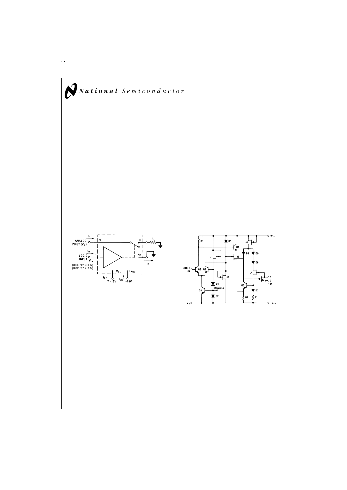
Test Circuit and Schematic Diagram
DS005667-2
FIGURE 1. Typical Circuit for One Switch
DS005667-12
FIGURE 2. Schematic Diagram (Normally Open)
January 1995
LF11331/LF13331/LF11332/LF13332/LF11333/LF13333/LF11201/LF13201/LF11202/LF13202 Quad
SPST JFET Analog Switches
© 1999 National Semiconductor Corporation DS005667 www.national.com
Page 2
Absolute Maximum Ratings (Note 1)
If Military/Aerospace specified devices are required,
please contact the National Semiconductor Sales Office/
Distributors for availability and specifications.
(Note 2)
Supply Voltage (V
CC−VEE
) 36V
Reference Voltage V
EE≤VR≤VCC
Logic Input Voltage VR−4.0V≤VIN≤VR+6.0V
Analog Voltage V
EE≤VA≤VCC
+6V;
V
A≤VEE
+36V
Analog Current |I
A
|<20 mA
Power Dissipation (Note 3)
Molded DIP (N Suffix) 500 mW
Cavity DIP (D Suffix) 900 mW
Operating Temperature Range
LF11201, 2 and LF11331, 2, 3 −55˚C to +125˚C
LF13201, 2 and LF13331, 2, 3 0˚C to +70˚C
Storage Temperature −65˚C to +150˚C
Soldering Information
N and D Package (10 sec.) 300˚C
SO Package:
Vapor Phase (60 sec.) 215˚C
Infrared (15 sec.) 220˚C
Electrical Characteristics (Note 4)
LF11331/2/3 LF13331/2/3
Symbol Parameter Conditions LF11201/2 LF13201/2 Units
Min Typ Max Min Typ Max
R
ON
“ON” Resistance V
A
=
0, I
D
=
1mA T
A
=
25˚C 150 200 150 250 Ω
200 300 200 350 Ω
R
ON
Match “ON” Resistance Matching T
A
=
25˚C 5 20 10 50 Ω
V
A
Analog Range
±10±
11
±10±
11 V
I
S(ON) +
Leakage Current in “ON” Condition Switch “ON,” V
S
=
V
D
=
±
10V T
A
=
25˚C 0.3 5 0.3 10 nA
I
D(ON)
3 100 3 30 nA
I
S(OFF)
Source Current in “OFF” Condition Switch “OFF,” V
S
=
+10V, T
A
=
25˚C 0.4 5 0.4 10 nA
V
D
=
−10V 3 100 3 30 nA
I
D(OFF)
Drain Current in “OFF” Condition Switch “OFF,” V
S
=
+10V, T
A
=
25˚C 0.1 5 0.1 10 nA
V
D
=
−10V 3 100 3 30 nA
V
INH
Logical “1” Input Voltage 2.0 2.0 V
V
INL
Logical “0” Input Voltage 0.8 0.8 V
I
INH
Logical “1” Input Current V
IN
=
5V T
A
=
25˚C 3.6 10
25
3.6 40
100
µA
I
INL
Logical “0” Input Current V
IN
=
0.8 T
A
=
25˚C 0.1 0.1 µA
11µA
t
ON
Delay Time “ON” V
S
=
±
10V, (
Figure 3
)T
A
=
25˚C 500 500 ns
t
OFF
Delay Time “OFF” V
S
=
±
10V, (
Figure 3
)T
A
=
25˚C 90 90 ns
t
ON−tOFF
Break-Before-Make V
S
=
±
10V, (
Figure 3
)T
A
=
25˚C 80 80 ns
C
S(OFF)
Source Capacitance Switch “OFF,” V
S
=
±
10V T
A
=
25˚C 4.0 4.0 pF
C
D(OFF)
Drain Capacitance Switch “OFF,” V
D
=
±
10V T
A
=
25˚C 3.0 3.0 pF
C
S(ON) +
Active Source and Drain Capacitance Switch “ON,” V
S
=
V
D
=
0V T
A
=
25˚C 5.0 5.0 pF
C
D(ON)
I
SO(OFF)
“OFF” Isolation (
Figure 4
), (Note 5) T
A
=
25˚C −50 −50 dB
CT Crosstalk (
Figure 4
), (Note 5) T
A
=
25˚C −65 −65 dB
SR Analog Slew Rate (Note 6) T
A
=
25˚C 50 50 V/µs
I
DIS
Disable Current (
Figure 5
), (Note 7) T
A
=
25˚C 0.4 1.0 0.6 1.5 mA
0.6 1.5 0.9 2.3 mA
I
EE
Negative Supply Current All Switches “OFF,” V
S
=
±
10V T
A
=
25˚C 3.0 5.0 4.3 7.0 mA
4.2 7.5 6.0 10.5 mA
I
R
Reference Supply Current All Switches “OFF,” V
S
=
±
10V T
A
=
25˚C 2.0 4.0 2.7 5.0 mA
2.8 6.0 3.8 7.5 mA
I
CC
Positive Supply Current All Switches “OFF,” V
S
=
±
10V T
A
=
25˚C 4.5 6.0 7.0 9.0 mA
6.3 9.0 9.8 13.5 mA
Note 1: “Absolute Maximum Ratings” indicate limits beyond which damage to the device may occur. Operating Ratings indicate conditions for which the device is
functional, but do not guarantee specific performance limits.
Note 2: Refer to RETSF11201X, RETSF11331X, RETSF11332X and RETSF11333X for military specifications.
Note 3: For operating at high temperature the molded DIP products must be derated based on a +100˚C maximum junction temperature and a thermal resistance
of +150˚C/W, devices in the cavity DIP are based on a +150˚C maximum junction temperature and are derated at
±
100˚C/W.
www.national.com 2
Page 3
Electrical Characteristics (Note 4) (Continued)
Note 4: Unless otherwise specified, V
CC
=
+15V, V
EE
=
−15V, V
R
=
0V, and limits apply for −55˚C≤T
A
≤+125˚C for the LF11331/2/3 and the LF11201/2,
−25˚C≤T
A
≤+85˚C for the LF13331/2/3 and the LF13201/2.
Note 5: These parameters are limited by the pin to pin capacitance of the package.
Note 6: This is the analog signal slew rate above which the signal is distorted as a result of finite internal slew rates.
Note 7: All switches in the device are turned “OFF” by saturating a transistor at the disable node as shown in
Figure 5
. The delay time will be approximately equal
to the t
ON
or t
OFF
plus the delay introduced by the external transistor.
Note 8: This graph indicates the analog current at which 1%of the analog current is lost when the drain is positive with respect to the source.
Note 9: θ
JA
(Typical) Thermal Resistance
Molded DIP (N) 85˚C/W
Cavity DIP (D) 100˚C/W
Small Outline (M) 105˚C/W
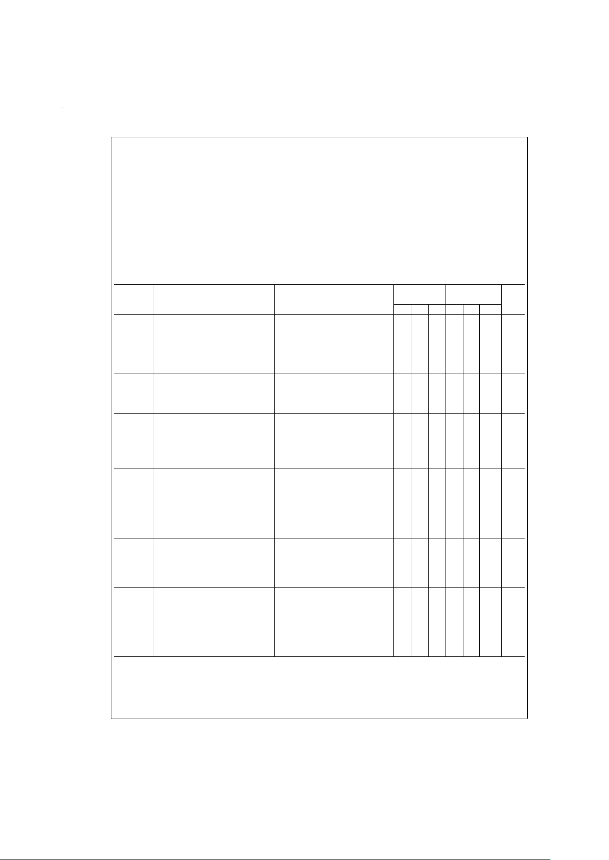
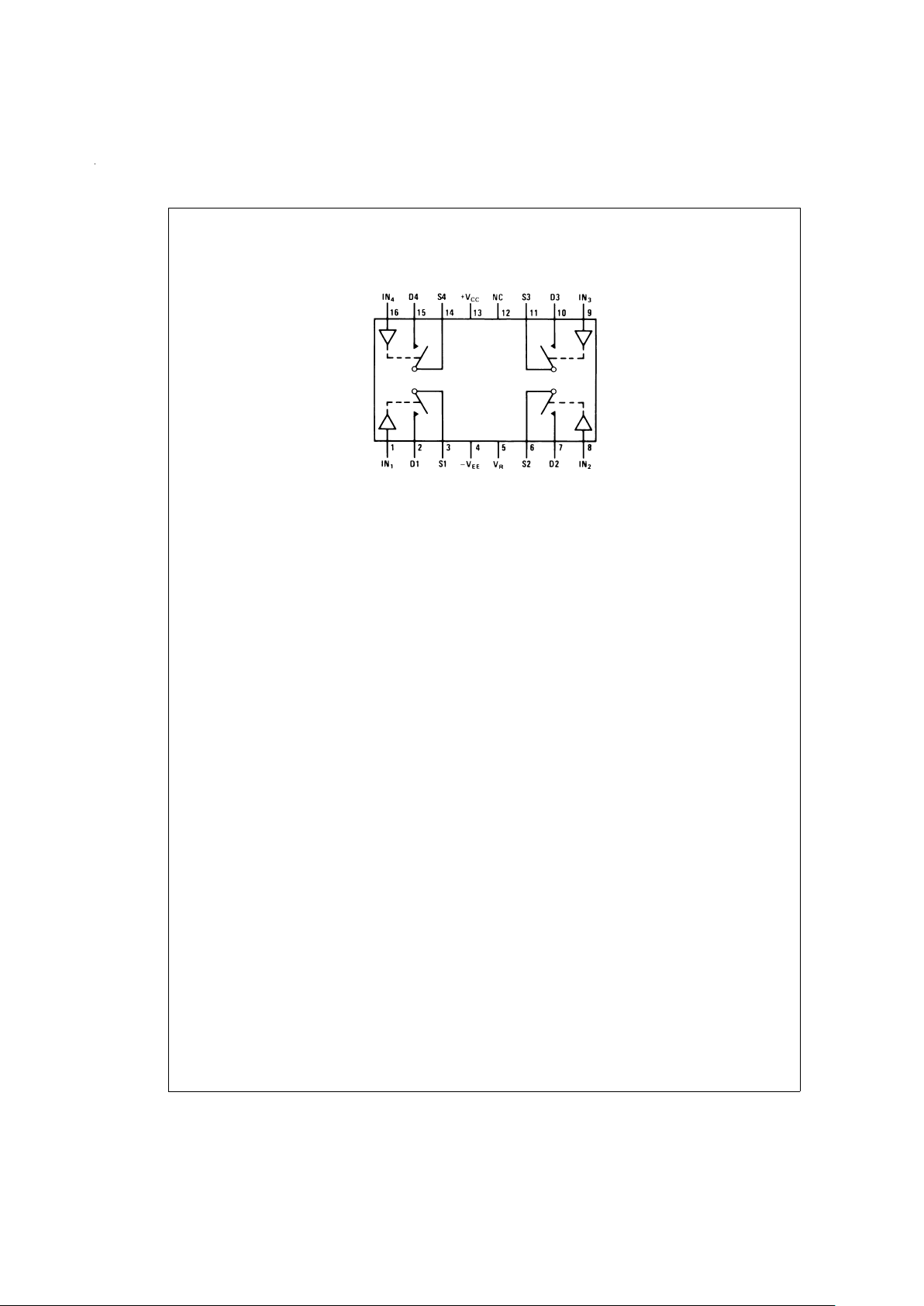
Connection Diagrams (Top View for SO and Dual-In-Line Packages) (All Switches Shown are For Logical “0”)
LF11331/LF13331
DS005667-1
LF11332/LF13332
DS005667-13
LF11333/LF13333
DS005667-14
LF11201/LF13201
DS005667-15
www.national.com3
Page 4
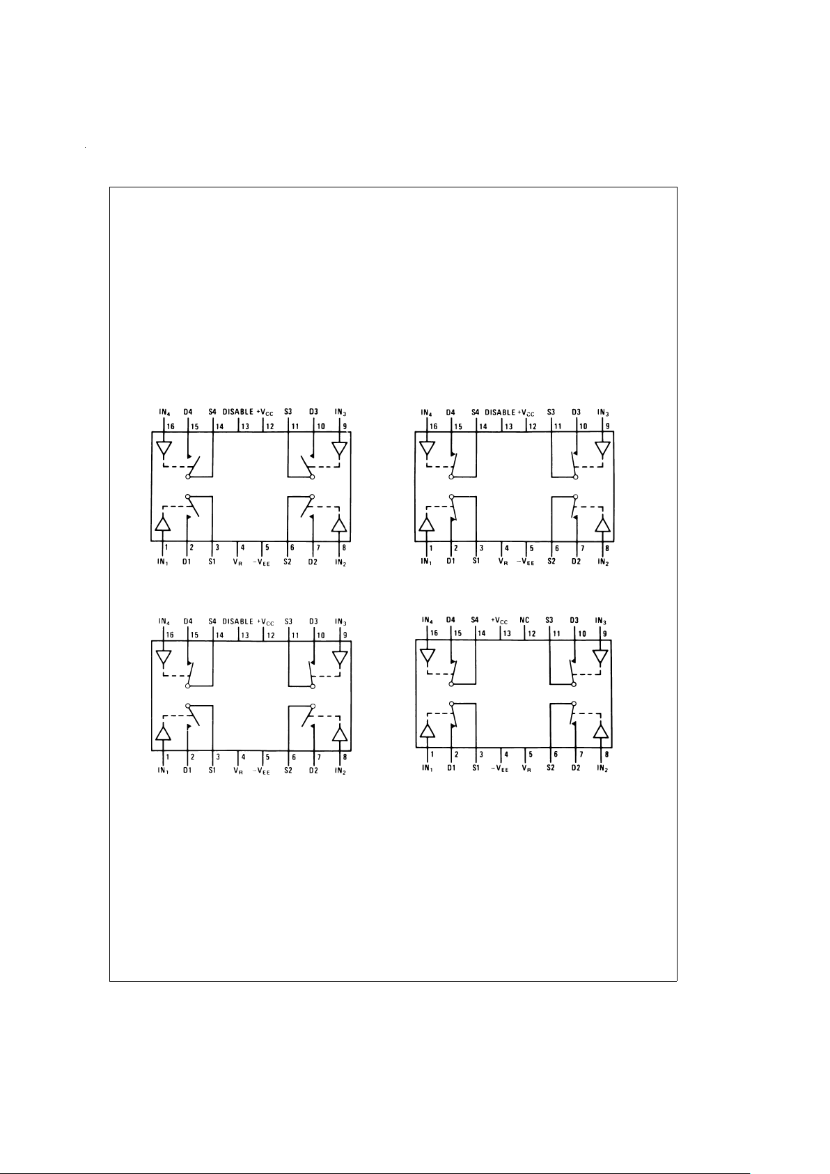
Connection Diagrams (Top View for SO and Dual-In-Line Packages) (All Switches Shown are For Logical
“0”) (Continued)
LF11202/LF13202
DS005667-16
Order Number LF13201D, LF11201D, LF11201D/883, LF13202D, LF11202D, LF11202D/883, LF13331D, LF11331D,
LF11331D/883, LF13332D, LF11332D, LF11332D/883, LF13333D, LF11333D or LH11333D/883
See NS Package Number D16C
Order Number LF13201M, LF13202M, LF13331M, LF13332M or LF13333M
See NS Package Number M16A
Order Number LF13201N, LF13202N, LF13331N, LF13332N or LF13333N
See NS Package Number N16A
www.national.com 4
Page 5
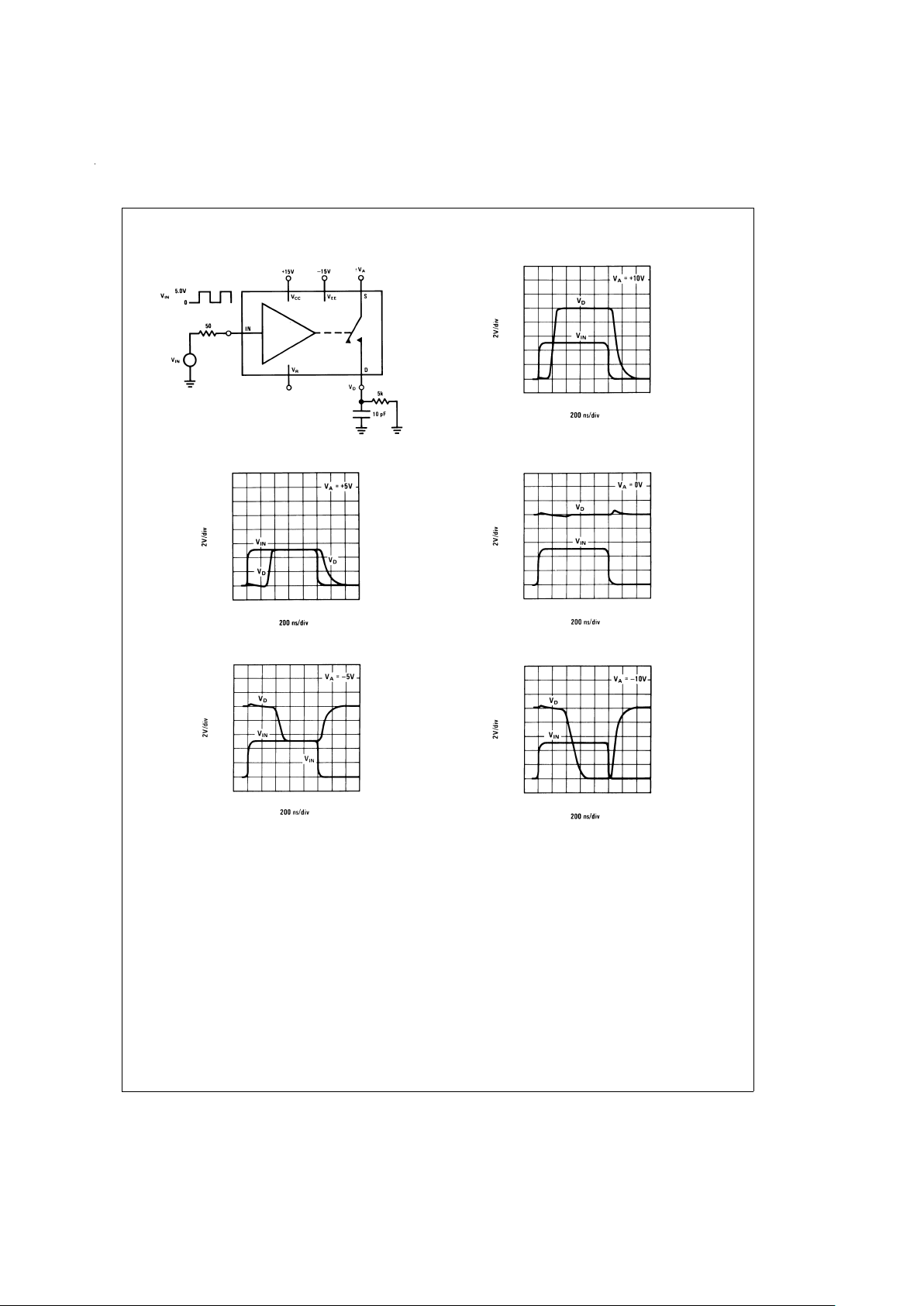
Test Circuit and Typical Performance Curves Delay Time, Rise Time, Settling Time, and
Switching Transients
DS005667-17
DS005667-18
DS005667-19
DS005667-20
DS005667-21
DS005667-22
www.national.com5
Page 6
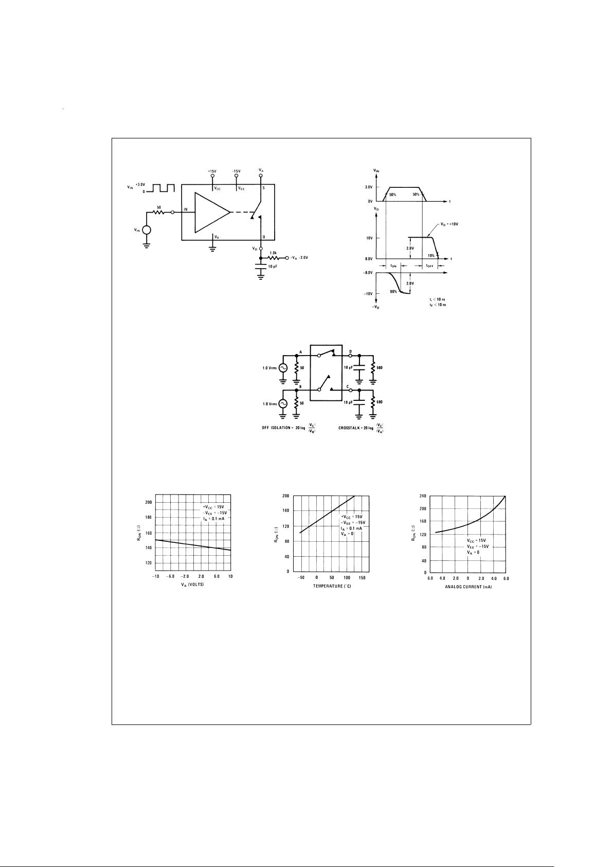
Additional Test Circuits
Typical Performance Characteristics
DS005667-39
DS005667-40
FIGURE 3. tON,t
OFF
Test Circuit and Waveforms for a Normally Open Switch
DS005667-41
FIGURE 4. “OFF” Isolation, Crosstalk, Small Signal Response
“ON” Resistance
DS005667-23
“ON” Resistance
DS005667-24
“ON” Resistance
DS005667-25
www.national.com 6
Page 7

Typical Performance Characteristics (Continued)
Break-Before-Make Action
DS005667-26
Switching Times
DS005667-27
Crosstalk and “OFF”
Isolation vs Frequency
Using Test Circuit of
Figure 5
DS005667-28
Supply Current
DS005667-29
Supply Current
DS005667-30
Supply Current
DS005667-31
Switch Leakage Currents
DS005667-32
Switch Leakage Current
DS005667-33
Switch Capacitances
DS005667-34
www.national.com7
Page 8

Typical Performance Characteristics (Continued)
Application Hints
GENERAL INFORMATION
These devices are monolithic quad JFET analog switches
with “ON” resistances which are essentially independent of
analog voltage or analog current. The leakage currents are
typically less than 1 nA at 25˚C in both the “OFF”and “ON”
switch states and introduce negligible errors in most applications. Each switch is controlled by minimum TTL logic levels
at its input and is designed to turn “OFF” faster than it will
turn “ON.” This prevents two analog sources from being transiently connected together during switching. The switches
were designed for applications which require
break-before-make action, no analog current loss, medium
speed switching times and moderate analog currents.
Because these analog switches are JFET rather than
CMOS, they do not require special handling.
LOGIC INPUTS
The logic input (IN), of each switch, is referenced to two forward diode drops (1.4V at 25˚C) from the reference supply
(V
R
) which makes it compatible with DTL, RTL, and TTL
logic families. For normal operation, the logic “0” voltage can
range from 0.8V to −4.0V with respect to V
R
and the logic “1”
voltage can range from 2.0V to 6.0V with respect to V
R
, pro-
vided V
IN
is not greater than (VCC−2.5V). If the input voltage
is greater than (V
CC
−2.5V), the input current will increase. If
the input voltage exceeds 6.0V or −4.0V with respect to V
R
,
a resistor in series with the input should be used to limit the
input current to less than 100µA.
ANALOG VOLTAGE AND CURRENT
Analog Voltage
Each switch has a constant “ON” resistance (R
ON
) for analog
voltages from (V
EE
+5V) to (VCC−5V). For analog voltages
greater than (V
CC
−5V), the switch will remain ON independent of the logic input voltage. For analog voltages less than
(V
EE
+5V), the ON resistance of the switch will increase. Although the switch will not operate normally when the analog
voltage is out of the previously mentioned range, the source
voltage can go to either (V
EE
+36V) or (VCC+6V), whichever
is more positive, and can go as negative as V
EE
without destruction. The drain (D) voltage can also go to either
(V
EE
+36V) or (VCC+6V), whichever is more positive, and can
go as negative as (V
CC
−36V) without destruction.
Analog Current
With the source (S) positive with respect to the drain (D), the
R
ON
is constant for low analog currents, but will increase at
higher currents (
>
5 mA) when the FET enters the saturation
region. However, if the drain is positive with respect to the
source and a small analog current loss at high analog currents (Note 6) is tolerable, a low R
ON
can be maintained for
analog currents greater than 5 mA at 25˚C.
Slew Rate of Analog
Voltage Above Which
Signal Loading Occurs
DS005667-35
Small Signal Response
DS005667-36
Maximum Accurate
Analog Current
vs Temperature
DS005667-37
Logical “1” Input Bias
Current
DS005667-38
www.national.com 8
Page 9

Application Hints (Continued)
LEAKAGE CURRENTS
The drain and source leakage currents, in both the ON and
the OFF states of each switch, are typically less than 1 nA at
25˚C and less than 100 nA at 125˚C.As shown in the typical
curves, these leakage currents are Dependent on power
supply voltages, analog voltage, analog current and the
source to drain voltage.
DELAY TIMES
The delay time OFF (t
OFF
) is essentially independent of both
the analog voltage and temperature. The delay time ON
(t
ON
) will decrease as either (VCC−VA) decreases or the tem-
perature decreases.
POWER SUPPLIES
The voltage between the positive supply (V
CC
) and either the
negative supply (V
EE
) or the reference supply (VR) can be as
much as 36V.To accommodate variations in input logic reference voltages, V
R
can range from VEEto (VCC−4.5V). Care
should be taken to ensure that the power supply leads for the
device never become reversed in polarity or that the device
is never inadvertently installed backwards in a test socket. If
one of these conditions occurs, the supplies would zener an
internal diode to an unlimited current; and result in a destroyed device.
SWITCHING TRANSIENTS
When a switch is turned OFF or ON, transients will appear at
the load due to the internal transient voltage at the gate of
the switch JFET being coupled to the drain and source by
the junction capacitances of the JFET. The magnitude of
these transients is dependent on the load. A lower value R
L
produces a lower transient voltage. A negative transient occurs during the delay time ON, while a positive transient occurs during the delay time OFF. These transients are relatively small when compared to faster switch families.
DISABLE NODE
This node can be used, as shown in
Figure 5
, to turn all the
switches in the unit off independent of logic inputs. Normally,
the node floats freely at an internal diode drop (≈0.7V) above
V
R
. When the external transistor in
Figure 5
is saturated, the
node is pulled very close to V
R
and the unit is disabled. Typically, the current from the node will be less than 1 mA. This
feature is not available on the LF11201 or LF11202 series.
Typical Applications
DS005667-6
FIGURE 5. Disable Function
Sample and Hold with Reset
DS005667-42
www.national.com9
Page 10

Typical Applications (Continued)
Programmable Inverting Non-Inverting Operational Amplifier
DS005667-43
Programmable Gain Operational Amplifier
DS005667-44
www.national.com 10
Page 11

Typical Applications (Continued)
Demultiplexer
DS005667-45
Multiplexer/Mixer
DS005667-46
www.national.com11
Page 12

Typical Applications (Continued)
8-Channel Analog Commutator with 6-Channel Select Logic
DS005667-47
Chopper Channel Amplifier
DS005667-48
www.national.com 12
Page 13

Typical Applications (Continued)
Self-Zeroing Operational Amplifier
DS005667-49
Programmable Integrator with Reset and Hold
DS005667-50
www.national.com13
Page 14

Typical Applications (Continued)
Staircase Transfer Function Operational Amplifier
DS005667-51
www.national.com 14
Page 15

Typical Applications (Continued)
DSB Modulator-Demodulator
DS005667-11
www.national.com15
Page 16

16
Page 17

Physical Dimensions inches (millimeters) unless otherwise noted
Order Number LF11201D, LF11201D/883, LF13201D, LF11202D, LF11202D/883, LF13202D, LF11331D,
LF11331D/883, LF13331D, LF11332D, LF11332D/883, LF13332D, LF11333D, LF11333D/883 or LF13333D
NS Package Number D16C
Order Number LF113201M, LF13202M,
LF13331M, LF13332M or LF13333M
NS Package Number M16A
www.national.com17
Page 18

Physical Dimensions inches (millimeters) unless otherwise noted (Continued)
LIFE SUPPORT POLICY
NATIONAL’S PRODUCTS ARE NOT AUTHORIZED FOR USE AS CRITICAL COMPONENTS IN LIFE SUPPORT DEVICES OR SYSTEMS WITHOUT THE EXPRESS WRITTEN APPROVAL OF THE PRESIDENT OF NATIONAL SEMICONDUCTOR CORPORATION. As used herein:
1. Life support devices or systems are devices or systems which, (a) are intended for surgical implant into
the body, or (b) support or sustain life,and whosefailure to perform when properly used in accordance
with instructions for use provided in the labeling, can
be reasonably expected to result in a significant injury
to the user.
2. A critical component is any component of a life support
device or system whose failure to perform can be reasonably expected to cause the failure of the life support
device or system, or to affect its safety or effectiveness.
National Semiconductor
Corporation
Americas
Tel: 1-800-272-9959
Fax: 1-800-737-7018
Email: support@nsc.com
www.national.com
National Semiconductor
Europe
Fax: +49 (0) 1 80-530 85 86
Email: europe.support@nsc.com
Deutsch Tel: +49 (0) 1 80-530 85 85
English Tel: +49 (0) 1 80-532 78 32
Français Tel: +49 (0) 1 80-532 93 58
Italiano Tel: +49 (0) 1 80-534 16 80
National Semiconductor
Asia Pacific Customer
Response Group
Tel: 65-2544466
Fax: 65-2504466
Email: sea.support@nsc.com
National Semiconductor
Japan Ltd.
Tel: 81-3-5639-7560
Fax: 81-3-5639-7507
Order Number LF13201N, LF13202N, LF13331N, LF13332N or LF13333N
NS Package Number N16A
LF11331/LF13331/LF11332/LF13332/LF11333/LF13333/LF11201/LF13201/LF11202/LF13202 Quad
SPST JFET Analog Switches
National does not assume any responsibility for use of any circuitry described, no circuit patent licenses are implied and National reserves the right at any time without notice to change said circuitry and specifications.
 Loading...