

Page 1
N-CHANNEL ENHANCEMENT-MODE LATERAL
MOSFETs
• EXCELLENT THERMAL STABILITY
• COMMON SOURCE CONFIGURATION
• P
= 60 W WITH 17.3 dB gain @ 945 MHz
OUT
• BeO FREE PACKAGE
• HIGH GAIN
• ESD PROTECTION
LET9060C
RF POWER TRANSISTORS
Ldmos Enhanced Technology
PRELIMINARY DATA
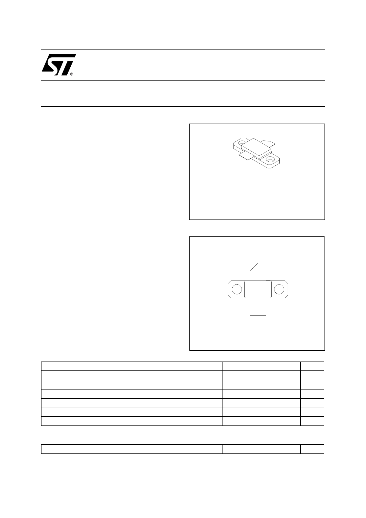
M243
epoxy sealed
DESCRIPTION
ORDER CODE
LET9060C
BRANDING
LET9060C
The LET9060C is an N-Channel enhancement-mode
lateral Field-Effect RF power transistor, designed for
high gain broadband, commercial and industrial
applications. It operates at 28 V in common source
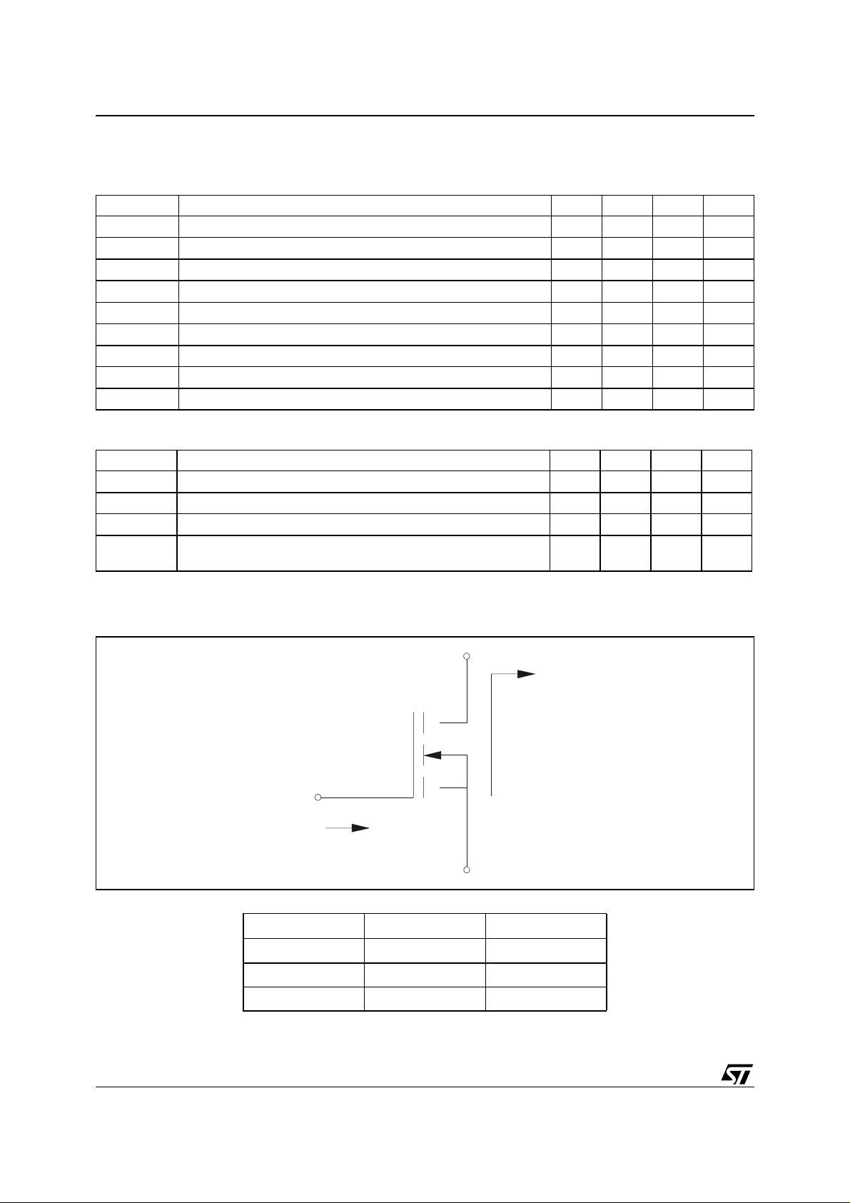
PIN CONNECTION
mode at frequencies up to 1.0 GHz. LET9060C
boasts the excellent gain, linearity and reliability of the
ST latest LDMOS technology. Its superior
1
performances make it an ideal solution for base
station applications.
3
2
1. Drain
2. Gate
ABSOLUTE MAXIMUM RATINGS (T
Symbol Parameter Value Unit
V
(BR)DSS
V
GS
I
D
P
DISS
Tj Max. Operating Junction Temperature 200 °C
T
STG
Drain-Source Voltage 65 V
Gate-Source Voltage -0.5 to +15 V
Drain Current 7 A
Power Dissipation (@ Tc = 70°C) 118 W
Storage Temperature -65 to +150 °C
CASE
= 25°C)
3. Source
THERMA L D ATA
R
th(j-c)
November, 4 2002
Junction -Case Thermal Resistance 1.1 °C/W
1/5
Page 2
LET9060C
ELECTRICAL SPECIFICATION (T
CASE
= 25°C)
STATIC
Symbol Test Conditions Min. Typ. Max. Unit
V
(BR)DSS
I
DSS
I
GSS
V
GS(Q)
V
DS(ON)
G
C
ISS
C
OSS
C
RSS
FS
VGS = 0 V IDS = 1 mA
VGS = 0 V VDS = 28 V
VGS = 5 V VDS = 0 V
VDS = 28 V
= 100 mA
ID
VGS = 10 V ID = 3 A
VDS = 10 V ID = 3 A
VGS = 0 V VDS = 28 V f = 1 MHz
VGS = 0 V VDS = 28 V f = 1 MHz
VGS = 0 V VDS = 28 V f = 1 MHz
65 V
1 µA
1 µA
2.0 5.0 V
0.7 0.8 V
2.3 mho
69.5 pF
38 pF
1.6 pF
DYNAMIC
Symbol Test Conditions Min. Typ. Max. Unit
P
1dB
G
P
η
D
Load
mismatch
VDD = 26 V IDQ = 250 mA f = 945 MHz
VDD = 26 V IDQ = 250 mA P
VDD = 26 V IDQ = 250 mA P
= 26 V IDQ = 250 mA P
V
DD
= 60 W f = 945 MHz
OUT
= 60 W f = 945 MHz
OUT
= 60 W f = 945 MHz
OUT
ALL PHASE ANGLES
60 65 W
17.3 dB
60 %
5:1 VSWR
IMPEDANCE DATA
Typical Input
Impedance
D
Z
DL
G
Zin
S
Z
FREQ.
925 MHz TBD TBD
945 MHz TBD TBD
960 MHz TBD TBD
(Ω) ZDL(Ω)
IN
Typical Drain
Load Impedance
2/5
Page 3
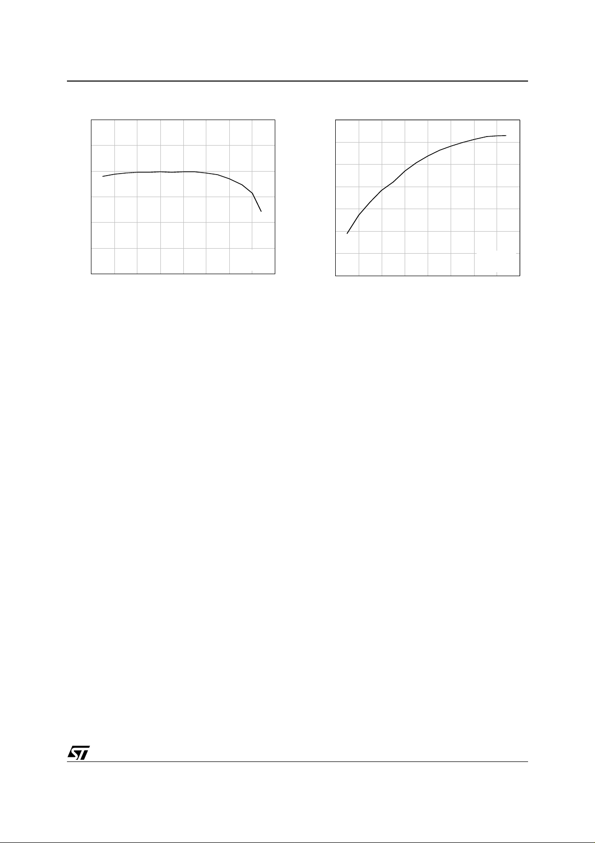
TYPICAL PERFORMANCE
Power Gain vs. Output Power
22
LET9060C
Efficiency vs. Output Power
70
20
18
16
Gp (dB)
14
12
10
0 1020304050607080
Pout (W)
f = 945 MHz
Vcc = 26 V
Idq = 250 mA
60
50
40
Eff (%)
30
20
10
0
0 1020304050607080
Pout (W)
f = 945 MHz
Vcc = 26 V
Idq = 250 mA
3/5
Page 4

LET9060C
M243 (.230 x .360 2L N/HERM W/FLG) MECHANICAL DATA
DIM.
A 5.21 5.72 0.205 0.225
B 5.46 6.48 0.215 0.255
C 5.59 6.10 0.220 0.240
D 14.27 0.562
E 20.07 20.57 0.790 0.810
F 8.89 9.40 0.350 0.370
G 0.10 0.15 0.004 0.006
H 3.18 4.45 0.125 0.175
I 1.83 2.24 0.072 0.088
J 1.27 1.78 0.050 0.070
MIN. TYP. MAX MIN. TYP. MAX
mm Inch
Controlling dimension: Inches 1022142E
4/5
Page 5

LET9060C
p
Information furnished is believed to be ac curate and reli able. Howev er, STMicroel ectronics assumes no responsibilit y for the cons equences
of use of such information nor for any infringement of patents or other rights of third parties which may result from its use. No license is granted
by implic ation or otherwise under any patent or patent rights of STMi croelectr onics. Specifications mentioned in thi s publicati on are s ubject
to change without notice. This publication supersedes and replaces all information previously supplied. STMicroelectronics products are not
authorized for use as cri tical comp onents in life support dev i ces or systems wi t hout express written ap proval of STMi croelect ronics.
The ST log o i s registered trademark of STMicroelectronics
2002 STMicroelectronics - All Right s Reserved
All other names are the property of their respective owners.
Australi a - Brazil - Canada - China - Fi nland - France - Germa ny - Hong Kong - India - Israel - Italy - Jap an -
Malaysia - Malta - Morocco - Singapore - Spain - Sweden - Switzerland - United Kingdom - U.S.A.
STMicroelectron ics GROUP OF COMPANIES
htt
://www.st.com
5/5
 Loading...