

Page 1
Designed for GSM / EDGE / IS-97 / WCDMA
applications
• EXCELLENT THERMAL STABILITY
• P
= 30 W with 11 dB gain @ 2170 MHz
OUT
• BeO FREE PACKAGE
• INTERNAL INPUT MATCHING
• ESD PROTECTION
LET21030C
RF POWER TRANSISTORS
Ldmos Enhanced Technology
TARGET DATA
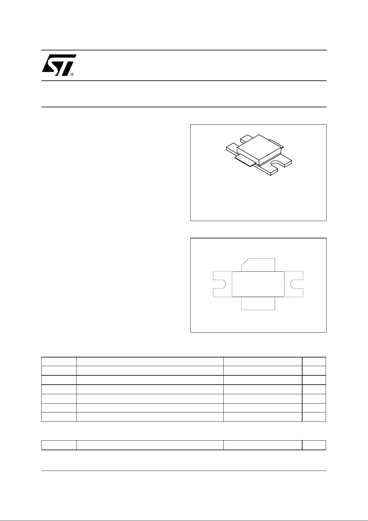
CASE 465E–03, STYLE 1
epoxy sealed
ORDER CODE
LET21030C
BRANDING
LET21030C
DESCRIPTION
The
LET21030C is a common s ource N-Channel
enhancement-mode lateral Field-Effect RF power
PIN CONNECTION
transistor designed for broadband commercial a nd
industrial applications at frequencies up to 2.1
GHz. The
LET21030C is design ed for high gain and
1
broadband performance operating in common
source mode at 26 V. Its internal matching makes
it ideal for base station applications requiring high
linearity.
2
ABSOLUTE MAXIMUM RATINGS (T
Symbol Parameter Value Unit
V
(BR)DSS
V
GS
I
D
P
DISS
Tj Max. Operating Junction Temperature 200 °C
T
STG
Drain-Source Voltage 65 V
Gate-Source Voltage -0.5 to +15 V
Drain Current 4 A
Power Dissipation (@ Tc = 70 °C) 65 W
Storage Temperature -65 to +200 °C
CASE
= 25 °C)
3
1. Drain
2. Gate
3. Source
THERMA L D ATA
R
th(j-c)
January, 24 2003
Junction -Case Thermal Resistance 2 °C/W
1/4
Page 2
LET21030C
ELECTRICAL SPECIFICATION (T
CASE
= 25 °C)
STATIC (Per Section)
Symbol Test Conditions Min. Typ. Max. Unit
V
(BR)DSS
I
DSS
I
GSS
V
GS(Q)
V
DS(ON)
G
FS
C
ISS
C
OSS
C
RSS
* Including input matching capaci tor in package ?
Symbol Test Conditions Min. Typ. Max. Unit
DYNAMIC (
P
mismatch
VGS = 0 V ID = 20 µA
VGS = 0 V VDS = 26 V
VGS = 5 V VDS = 0 V
VDS = 28 V ID = TBD
VGS = 10 V ID = 1 A
VDS = 10 V ID = 1 A
*VGS = 0 V VDD = 26 V f = 1 MHz
VGS = 0 V VDD = 26 V f = 1 MHz
VGS = 0 V VDS = 26 V f = 1 MHz
f = 2170 MHz
(1)
OUT
(1)
η
D
Load
)
VDD = 26 V IDQ = TBD
VDD = 26 V IDQ = TBD
= 26 V P
V
DD
OUT
= 30 W
ALL PHASE ANGLES
65 V
1 µA
1 µA
2 4.5 V
0.29 0.4 V
2 mho
TBD pF
TBD pF
TBD pF
30 35 W
45 50 %
10:1 VSWR
DYNAMIC (
P
OUT(W-CDMA)
η
D(W-CDMA)
(1) 1 dB Compression point
(2) +/- 5 MHz offset; 3.84 MHz Bandwitdh
f = 2110 - 2170 MHz
(1)
P
OUT
(1)
η
D
G
P
(2)
(2)
)
VDD = 26 V IDQ = TBD
VDD = 26 V IDQ = TBD
VDD = 26 V IDQ = TBD mA P
OUT
= 30 W
ACPR -45 dBc 5 W
ACPR -45 dBc 20 %
25 30 W
40 45 %
11 dB
ESD PROTECTION CHARACTERISTICS
Test Conditions Class
Human Body Model 2
Machine Model M3
2/4
Page 3
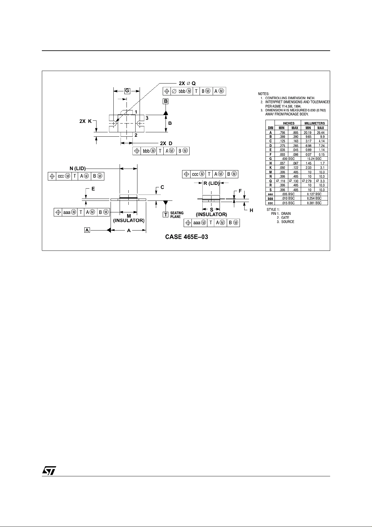
465E-03 MECHANICAL DAT A
LET21030C
3/4
Page 4

LET21030C
Information furnished is believed to be accurate an d rel i able. Howev er, STMicroel ectronics assumes no resp onsibility for the cons equences
of use of such information nor for any infringement of patents or other rights of third parties which may result from its use. No license is granted
by implic ation or otherwise under any patent or patent rights of STMi croelectr onics. Sp ecifications mentioned in thi s publicati on are subject
to change without notice. This publication supersedes and replaces all information previously supplied. STMicroelectronics products are not
authorized for use as cri tical comp onents in life support dev i ces or systems wi thout exp ress written approval of STM i croelect ronics.
The ST log o i s registered trademark of STMicroelectronics
2003 STMicroelectronic s - All Rights Reserved
All other names are the property of their resp ective owner s.
Australi a - Brazil - Ca nada - China - Finland - France - Germany - Hong Kong - India - Israel - Italy - Japan -
Malaysia - Malta - Morocco - Singapore - Spain - Sweden - Switzerland - United Kingdom - U.S.A.
http://www.st.com
4/4
 Loading...