

Page 1
1/4June 2002
■
RF REGULATOR
■
VERY LOW DROPOUT VOLTAGE : 50mV
■
VERY LOW CONSUMPTION : 320µA FULL
LOAD
■
VERY GOOD TRANSIENT BEHAVIOUR : 1mV
■
OUTPUT CURRENT : 200mA
■
HIGH PSRR : 65dB
■
NO CURRENT IN POWER DOWN MODE
■
SHORT CIRCUIT PROTECTION
TYPICAL APPLICATIONS
– Cellular and Cordless phones suppli ed by 1 cell
Lithium-ion battery / 3 cells Ni-MH or Ni-Cd
battery
– PDA (Personal Digital Assistant),
– Smart phone
– Portable equipm ent
– Supply for RF devices for cellular phone
APPLICATION NOTE
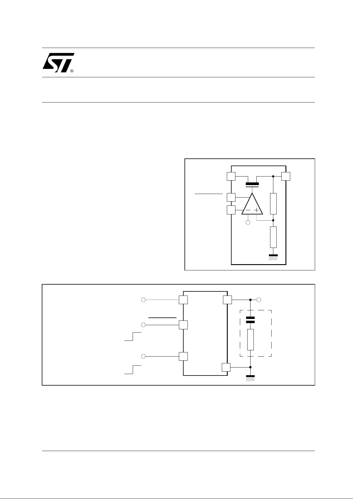
An external capacitor (C
OUT
= 1µF) with an
equivalent serial resistance (ESR) in the range
0.02 to 0.6Ω is used for regulator stability.
Figure 1 :
Block Diagram
?
V
REF
?
?
?
LDO_514
OUTIN
PWRDWN
STDBY
Figure 2 :
Typical Application Circuit
1µF
ESR
V
OUT
C
OUT
?
?
OUT
GND
?
?
?
V
IN
IN
PWRDWN
Power Down Mode
OFF
ON
Stand-by Mode
STDBY
Active Mode
LDO_514
→
→
Stand-by Mode
→
→
LDO_514
This is advance information on a new product now in development or undergoing evaluation. Details are subject to change without noti ce.
PRODUCT PREVIEW
IP Library: High PSRR, Very Low power,
200mA Low Dropout Volt age Regulator
Page 2
LDO_514
2/4
ELECTRICAL CHARACTERISTICS
3V < V
IN
< 5.5V, -55°C < TA < +125°C, C
OUT
= 1µF ±20%, 20mΩ < ESR < 0.6Ω, I
LOAD
= 200mA.
Typical case : V
IN
= 4V, T = 25°C, C
OUT
= 1µF.
Notes: 1. Above characteristics are given for 3V minimum input operating range voltage, but regulator is
operational with 2.7V minimum input voltage.
2. All parameters are guaranteed with 170mV min Dropout voltage.
Parameter Symbol Test Condition Min. Typ. Max. Unit
Input Voltage Range (Note 1) V
IN
3 5.5 V
Output Voltage V
OUT
2.8 V
Output Voltage Accuracy 3 %
Output current I
OUT
200 mA
Dropout Voltage ∆V
DO
∆V
OUT
= 50mV,
I
LOAD
= 200mA
50 mV
(Note 2) 170
Quiescent current I
Q
I
LOAD
= 100µA 70 110 µA
I
LOAD
= 20mA 90 130
I
LOAD
= 200mA 320 440
Power down mode quiescent
current
I
QPDM
Power down active 100 nA
Power Supply Rejection Ratio PSRR DC 65 dB
f = 10KHz 60
f = 100KHz 50
Line Regulation L
IR
I
LOAD
= 200mA,
V
IN
= 3V to 5.5V
1.5 2.5 mV
Load Regulation L
DR
I
LOAD
= 100µA - 200mA 35 40 mV
Line Transient L
IRT
∆V
IN
= 300mV
t
RISE
= t
FALL
= 10µs
<1 mV
Load Transient L
DTR
I
LOAD
= 100µA - 200mA
in 10µs
0.5 1 mV
Output Noise Voltage en 100Hz 1400
1KHz 450
10KHz 150
en
RMS
BW : 100Hz to 100KHz 45 µV
RMS
Output decoupling Capacitor C
OUT
1µF
Settling time I
LOAD
= 200mA 15 30 µs
Short Circuit Current Limit I
SHORT
800 mA
nV
Hz
----------- -
Page 3

LDO_514
3/4
10 60 110 160 210
2710
2720
2730
2740
2750
OUTPUT CURRENT (mA)
OUTPU T VOLTAGE (mV)
Vin=5.5V
Vin=4.0V
Vin=3.0V
2795
2797
2799
2801
2803
2805
INPUT VOLTAGE (V)
OUTPUT VOLTAGE (mV)
3.00 3.20 3.40 3.50 3.80 4.00 4.50 5 5.1
Full Load
1
10
100
1000
10000
100000
1000000
10000000
-65
-55
-45
-35
-25
-15
FREQUEN CY (Hz)
PSRR (dB)
170mV
200mV
2V
150mV
ELECTRICAL CHARACTERISTICS : STAND-BY MO DE
3V < V
IN
< 5.5V, -30°C < TA < +85°C, V
REF
= 2.8V, C
OUT
= 4.7µF ±20%, 20mΩ < ESR < 0.6Ω.
I
LOAD
= 500µA.
Typical case : V
IN
= 4V, Ambient temperature, I
LOAD
= 500µA.
TYPICAL CHARACTERISTICS
Parameter Symbol Test Condition Min. Typ. Max. Unit
Output current in stand-by mode I
OUTSTDBY
200 µA
Quiescent Current in stand-by mode I
STDBY
I
LOAD
= 500µA 15 20
Power Supply Rejection Ratio in
stand-by mode
PSRR
STY
f = 10KHz 55 dB
Line Regulation in stand-by mode Lir
STBY
VIN = 3V to 5.5V 2 mV
Load Regulation in stand-by mode Ldr
STBY
I
LOAD
= 100µA - 500µA 1 mV
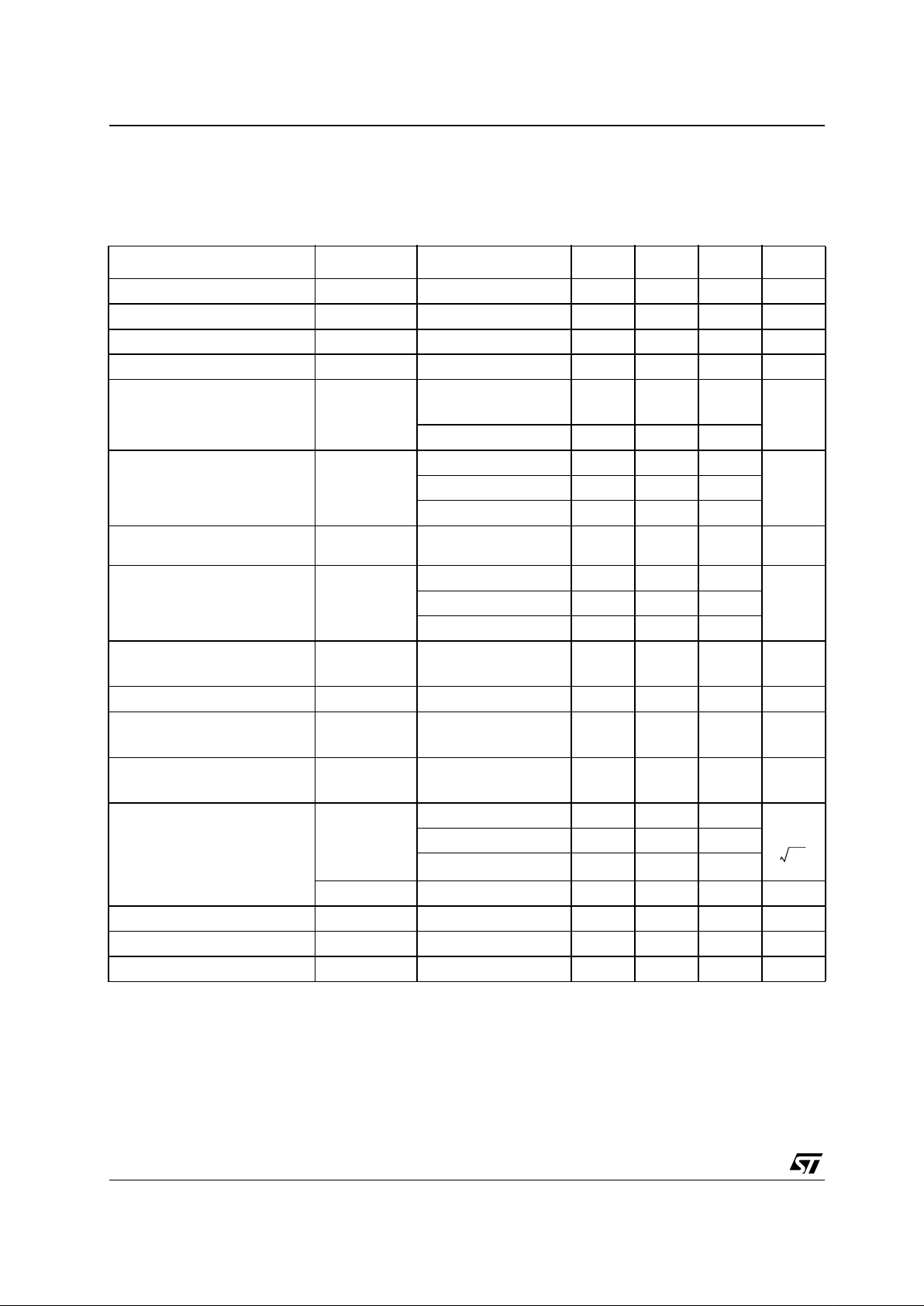
Figure 3 :
PSRR vs Freq for Various Voltage Drop
(V
OUT
= 2.8V, Full Load)
Figure 4 :
Output Voltage vs. Input Voltage
(V
OUT
= 2.8V, Full Load)
Figure 5 :
Output Voltage vs Output Current (Load Regulation)
Page 4

4/4
LDO_514
Information furnished is bel ieved to be accurate and reliable. However, STMicroe lectronics assumes no responsibility for the
consequences of use of such information nor for any infringement of patents or other rights of third parties which may result from
its use. No li cense is granted by imp lication or otherwise under a ny patent or patent rig hts of STMicroelectronics. Specificat ions
mentioned in this publication ar e subject to change without notice. This publication supersedes and replaces all information
previously supplied. S TMicroelectronics products are not authorized for use as critica l components in life suppo rt devices or
systems without express written approval of STMicroelectronics.
The ST logo is a registered trademark of STMicroelectronics
© 2002 STMicroelectronics - All Rights Reserved
STMicroele ct ronics GROUP OF COM P A NI E S
Australia - Brazil - Canada - China - F i nl and - France - Germany - Hong Kong - Indi a - Israel - Ital y - J apan - Malays i a - M a l ta - Morocco
Singapor e - S pai n - Sweden - Switzerland - U ni ted Kingdom - United States
http://www.st.com
 Loading...