

Page 1
Class A
Compression Amplifier
LD511 DATA SHEET
FEATURES
• 64 dB typical electrical gain
• 0.94 V
DC voltage regulator
• 7 ms attack time, 40 ms release time
• 15 dB threshold adjustment
• low noise and distortion
• compression ratio
∞ : 1
• 0.3 kHz - 6 kHz frequency response
STANDARD PACKAGING
• 10 pin MICROpac
• 10 pin MINIpac
• 10 pin PLID
®
• 10 pin SLT
• Chip (59 x 59 mils)
Au Bump
DESCRIPTION
The LD511 is a Class A compression amplifier which can
operate over a range of DC battery voltages from 1.1 V
to 2.4 V. A voltage regulator, which is independent of supply
voltage variations, is on-chip to supply a stable 0.94 V
DC bias
to the amplifier circuitry and to the microphone.
The LD511, in compression, has approximately 15 dB of
threshold adjustment by varying
R
(see application circuit)
TH
and a compression function ratio of ∞ : 1.
Minimum attack and release times are fixed at 7 ms and 40 ms
respectively and they can be adjusted simultaneously by
changing the filter capacitor on pin 8, although the ratio of
attack to release time is kept constant.
The output stage bias can be set to accommodate different
receiver impedances by changing the value of
voltage across
R
(pin 2 to ground) is a constant 27 mV so the
E
bias current is 27 mV divided by the total value of
R
E
R
in parallel
E
. The
with 500 Ω.
V
REG
A IN
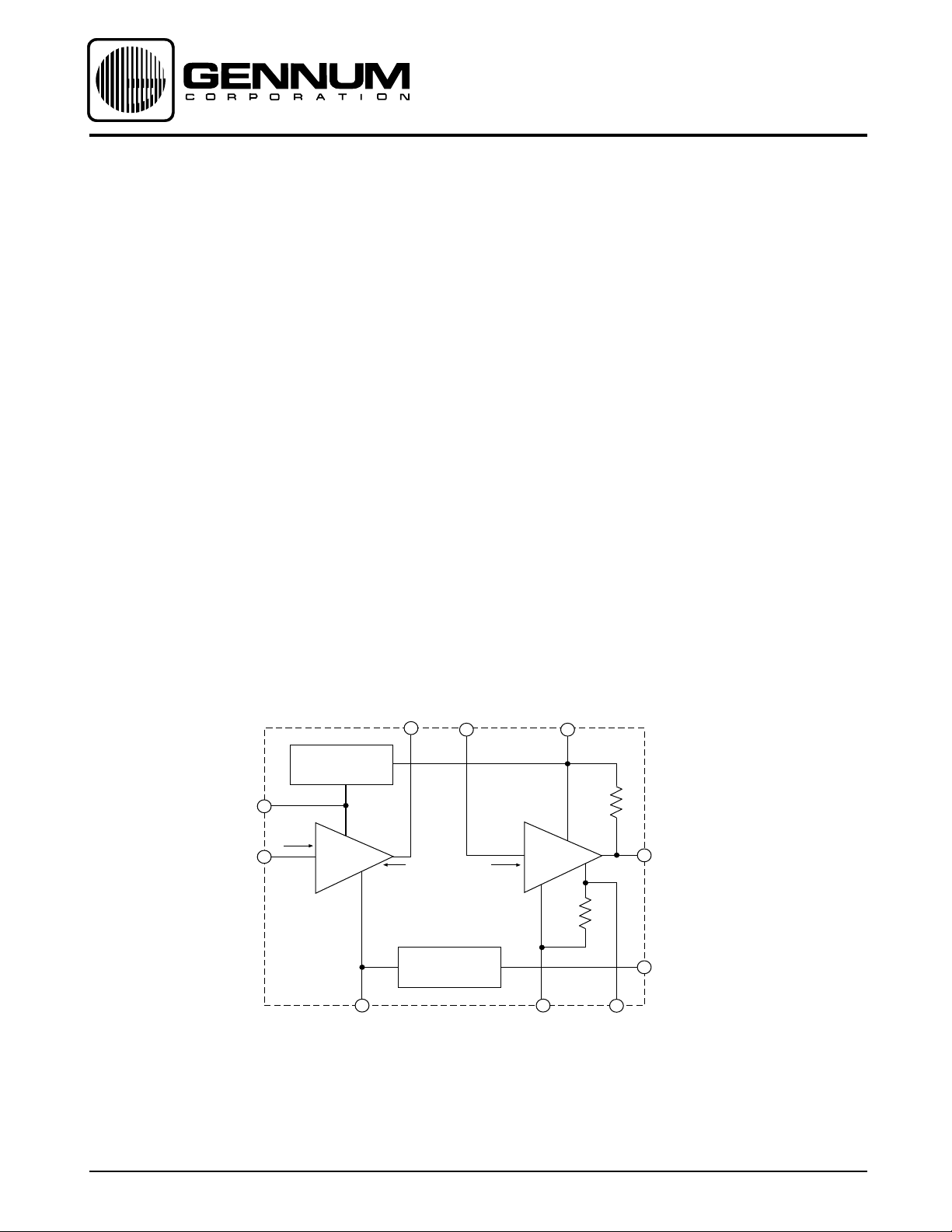
Revision Date: January 2001
A OUT B IN V
10
VOLTAGE
REGULATOR
7
9
All resistors in ohms, all capacitors
in farads unless otherwise stated
- A
R
IN
8
C
AGC
BLOCK DIAGRAM
1
10K 35K
RECTIFIER
- B
GND
B
6
20K
3
B OUT
R
E
5
AGC
24
R
E
500 - 32 - 11
GENNUM CORPORATION P.O. Box 489, Stn. A, Burlington, Ontario, Canada L7R 3Y3 tel. +1 (905) 632-2996
Web Site: www.gennum.com E-mail: hipinfo@gennum.com
Page 2
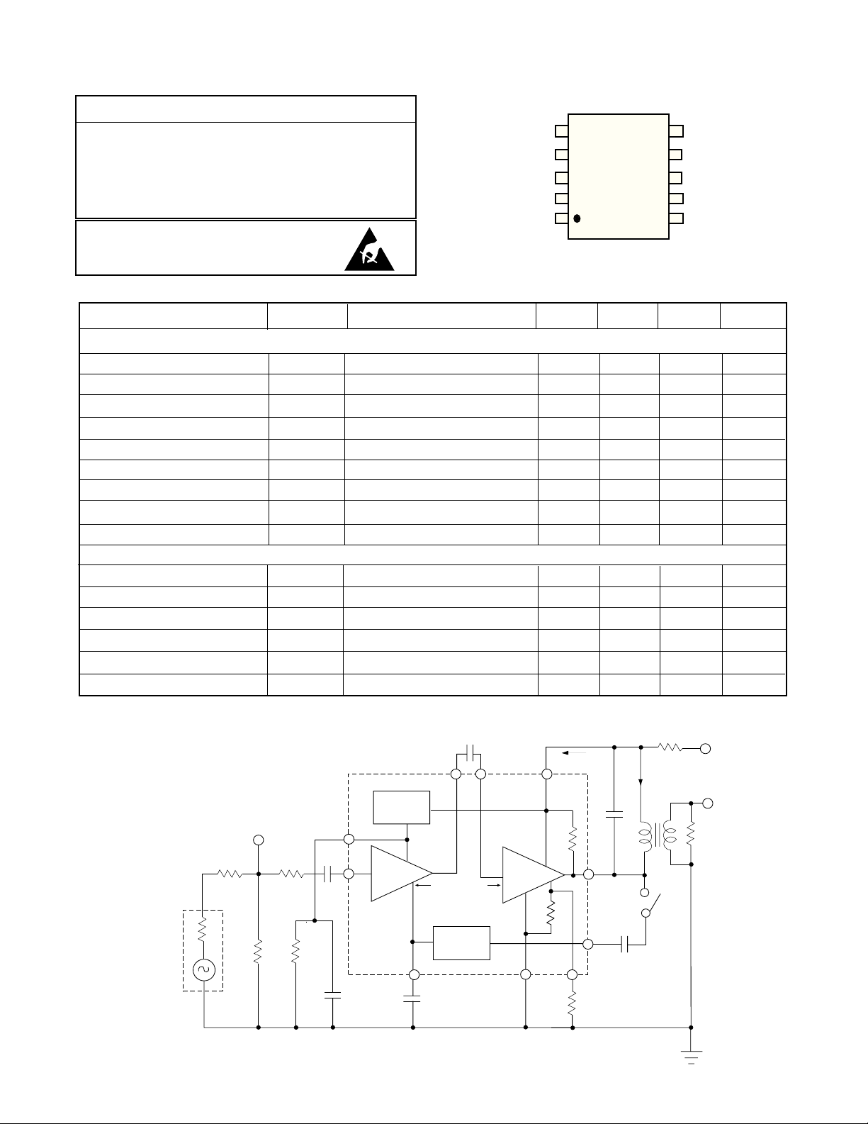
ABSOLUTE MAXIMUM RATINGS
PARAMETER VALUE/UNITS
Supply Voltage 2.4 V DC
Power Dissipation 25 mW
Operating Temperature Range -10°C to 40° C
Storage Temperature Range -20°C to 70° C
CAUTION
CLASS 1 ESD SENSITIVITY
AGC
GND
B OUT
R
B IN
PIN CONNECTION
5
E
6
V
B
V
REG
C
AGC
A IN
101
A OUT
ELECTRICAL CHARACTERISTICS Conditions: Frequency = 1 kHz, Temperature = 25°C, Supply Voltage V
= 1.3 VDC
B
PARAMETER SYMBOL CONDITIONS MIN TYP MAX UNITS
COMPRESSION INACTIVE (S1 OPEN)
Gain A
V
60 64 68 dB
Input Referred Noise IRN NFB 0.2 - 10kHz at 12 dB/oct - 2.0 4.0 µV
Total Harmonic Distortion THD - 1 3 %
Amplifier Current I
Transducer Current I
Input Impedance R
Regulated Voltage V
On Chip Emitter Resistance R
Emitter Bias Voltage (pin 2) V
AMP
TRANS
IN
REG
E
RE
- 0.4 0.6 mA
1.35 1.6 2.0 mA
-15 -kΩ
0.90 0.96 1.0 VDC
- 500 - Ω
-27 -mV
COMPRESSION ACTIVE (S1 CLOSED)
Compression Range - ∞ -dB
Total Harmonic Distortion THD
Attack Time T
Release Time T
Compression Output V
Compression Output Change ∆V
COMP
ATT
REL
COMPOUT
COMPOUTV2
All parameters and switches remain as shown in Test Circuit unless otherwise stated in CONDITIONS column
Notes: 1. ∆V
COMPOUT
R
50
= V
56K
S
OUT[V2
V2
=120mV] - V
3.9K
27K
56
V2 = 1 mV - 4.0 7.0 %
V2 switched from 112µV to 2 mV - 7 - ms
-40 -ms
V2 = 1 mV - 0.10 0.18 VRMS
= 120 mV; Note 1 - 13 20 mVRMS
COMPOUT
C
S
0.047
7
9
VOLTAGE
REGULATOR
- A
84
0.033
10K 35K
RECTIFIER
I
AMP
110
- B
6
0.068
20K
3
R
E
5
2
0.0047
S1
R
B
4.7
I
TRANS
Hammond
99966
VB=1.3 VDC
V
OUT
R
L
600
500 - 32 - 11
10
All resistors in ohms, all capacitors in farads unless otherwise stated
2.2
Fig. 1 Test Circuit
2
15
Page 3

107
6
80
10K
20K
9
10
0.1
All resistors in ohms, all capacitors
in farads unless otherwise stated
15K
8
5
1
Fig. 2 Functional Schematic
R
VC
VOLTAGE
REGULATOR
7
9
- A
10K
10K 35K
RECTIFIER
8
2.2
0.1
110
- B
42
6
20K
R
Fig. 3 LD511 Stand Alone Application Circuit
32K
3.2K
All resistors in ohms, all capacitors
in farads unless otherwise stated
VB=1.3 VDC
ED1913
3
R
TH
100K
E
5
4.7n
47
0.068
3
2
500
4
R
VC
10K
VOLTAGE
REGULATOR
7
10
9
0.1
- A
10K 35K
RECTIFIER
84
2.2
0.1
- B
6
20K
MPO
50K
3
R
E
5
0.0047
2
100K
All resistors in ohms, all capacitors
in farads unless otherwise stated
110
VB=1.3 VDC
1.0
EP3075
0.1
R
TH
Fig. 4 LD511/Class D Application Circuit
3
500 - 32 - 11
Page 4

0
63
-0.1
-0.2
-0.3
-0.4
REGULATOR VOLTAGE GAIN(dB)
-0.5
0 10 20 30 40 50 60 70 80 90 100
BATTERY RESISTANCE (Ω)
Fig. 5 Voltage Gain vs Battery Resistance
2.5
2.0
1.5
1.0
TOTAL CURRENT (mA)
0.5
0
0.9 1.0 1.1 1.2 1.3 1.4 1.5 1.6 1.7 1.8
BATTERY VOLTAGE (V)
Fig. 7 Total Current vs Battery Voltage
1000
500
200
100
OUTPUT VOLTAGE (mV)
RTH = ∞
50
20
10
5
2
0.01 0.1 1.0 10 100
RTH = 200k
RTH = 100k
RTH = 0k
INPUT VOLTAGE (mV)
Fig. 9 Threshold Adjustment
62
61
60
VOLTAGE GAIN (dB)
59
58
0.8 0.9 1.0 1.1 1.2 1.3 1.4 1.5 1.6 1.7
BATTERY VOLTAGE (V)
Fig. 6 Voltage Gain vs Battery Voltage
0.95
0.93
0.91
0.89
0.87
REGULATOR VOLTAGE (VDC)
0.85
0.9 1.1 1.3 1.5 1.7
BATTERY VOLTAGE (V)
Fig. 8 Regulator Voltage vs Battery Voltage
4
2
0
-2
-4
-6
-8
-10
-12
-14
-16
RELATIVE OUTPUT (dB)
-18
-20
CS = 47nF
= 22nF
C
S
= 10nF
C
S
= 6.8nF
C
S
20 20k
FREQUENCY (Hz)
Fig. 10 Frequency Response at Various
CS Values
GENNUM CORPORATION
MAILING ADDRESS:
P.O. Box 489, Stn. A, Burlington, Ontario, Canada L7R 3Y3
Tel. +1 (905) 632-2996 Fax +1 (905) 632-2814
SHIPPING ADDRESS:
970 Fraser Drive, Burlington, Ontario, Canada L7L 5P5
GENNUM JAPAN CORPORATION
C-101, Miyamae Village, 2-10-42 Miyamae, Suginami-ku, Tokyo 168-0081,
DOCUMENT IDENTIFICATION: DATA SHEET
The product is in production. Gennum reserves the right to make
changes at any time to improve reliability, function or design, in
order to provide the best product possible.
REVISION NOTES:
Changes to standard packaging information
Japan Tel. +81 (3) 3334-7700 Fax: +81 (3) 3247-8839
Gennum Corporation assumes no responsibility for the use of any circuits described herein and makes no representations that they are free from patent infringement.
500 - 32 - 11
© Copyright November 1980 Gennum Corporation. All rights reserved. Printed in Canada.
4
 Loading...