

Datasheet LD2981CM30TR, LD2981CM50TR, LD2981CM48TR, LD2981CM38TR, LD2981CM33TR Datasheet (SGS Thomson Microelectronics)
...Page 1
LD2981
VOLTAGE REGULATORS WITH INHIBIT
■ ULTRALOWDROPOUTVOLTAGE
(0.2VAT100mALOAD,7mVAT1mA LOAD)
■ VERYLOWQUIESCENTCURRENT
(MAX1µA WHENISIN SHUTDOWNMODE)
■ OUTPUT CURRENT UP TO100mA
■ LOGIC-CONTROLLEDELECTRONIC
SHUTDOWN
■ OUTPUT VOLTAGESOF 2.85;3.0;3.2;3.3;
3.8;4.85; 5.0V
■ INTERNALCURRENT AND THERMALLIMIT
■ AVAILABLEIN± 0.75%TOLLERANCE(AT
o
25
C, A VERSION)
■ OUTPUT LOWNOISEVOLTAGE160µVrms
■ ONLY4.7µF FOR STABILITY
■ TEMPERATURERANGE:-40 TO 125
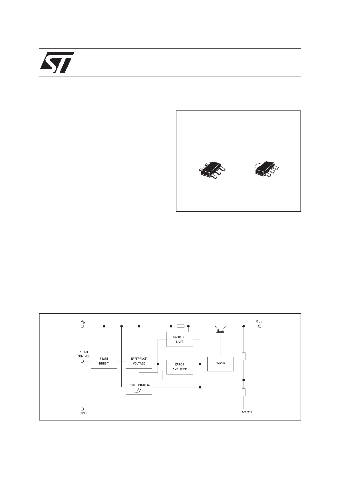
■ SMALLESTPACKAGESOT23-5LAND
SOT-89
■ FASTDYNAMICRESPONCETO LINEAND
LOADCHANGES
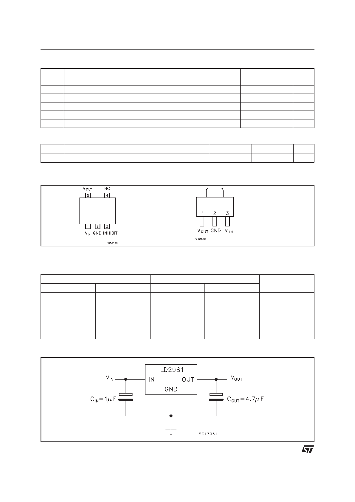
DESCRIPTION
The LD2981 series are 100mA fixed-output
voltage regulator. The ultra drop-voltage and the
ultralow quiescentcurrent make them particularly
suitablefor low noise, lowpower applications and
in battery poweredsystems.
o
C
SERIES
VERY LOW DROP
SOT23-5L SOT-89
In sleep mode quiescent current is less than 1µA
when INHIBIT pis is pulled low. Shutdown Logic
Control function is available on pin n.3 (TTL
compatible). This means that when the device is
used aslocal regulator,it ispossible to put a part
of the board in standby, decreasing the total
power consumption. Typlical application are in
cellular phone, palmtop/laptop computer,
personal digital assistant (PDA), personalstereo,
camcorderand camera.
SCHEMATIC DIAGRAM
April 2000
1/12
Page 2
LD2981
ABSOLUTE MAXIMUM RATING
Symbol Parameter Value Unit
V
DC InputVoltage 16 V
IN
V
THERMALDATA
Symbol Parameter SOT-89 SOT23-5L Unit
R
thj-cas e
INHBITInput Voltage 16 V
INH
OutputCurrent Internally limited mA
I
o
P
PowerDissipation Internally limited mW
tot
StorageTemperature Range - 55 to 150
T
stg
OperatingJunctionTemperatureRange - 40 to 125
T
op
Thermal ResistanceJunction-case 15 81
o
o
C
o
C
C/W
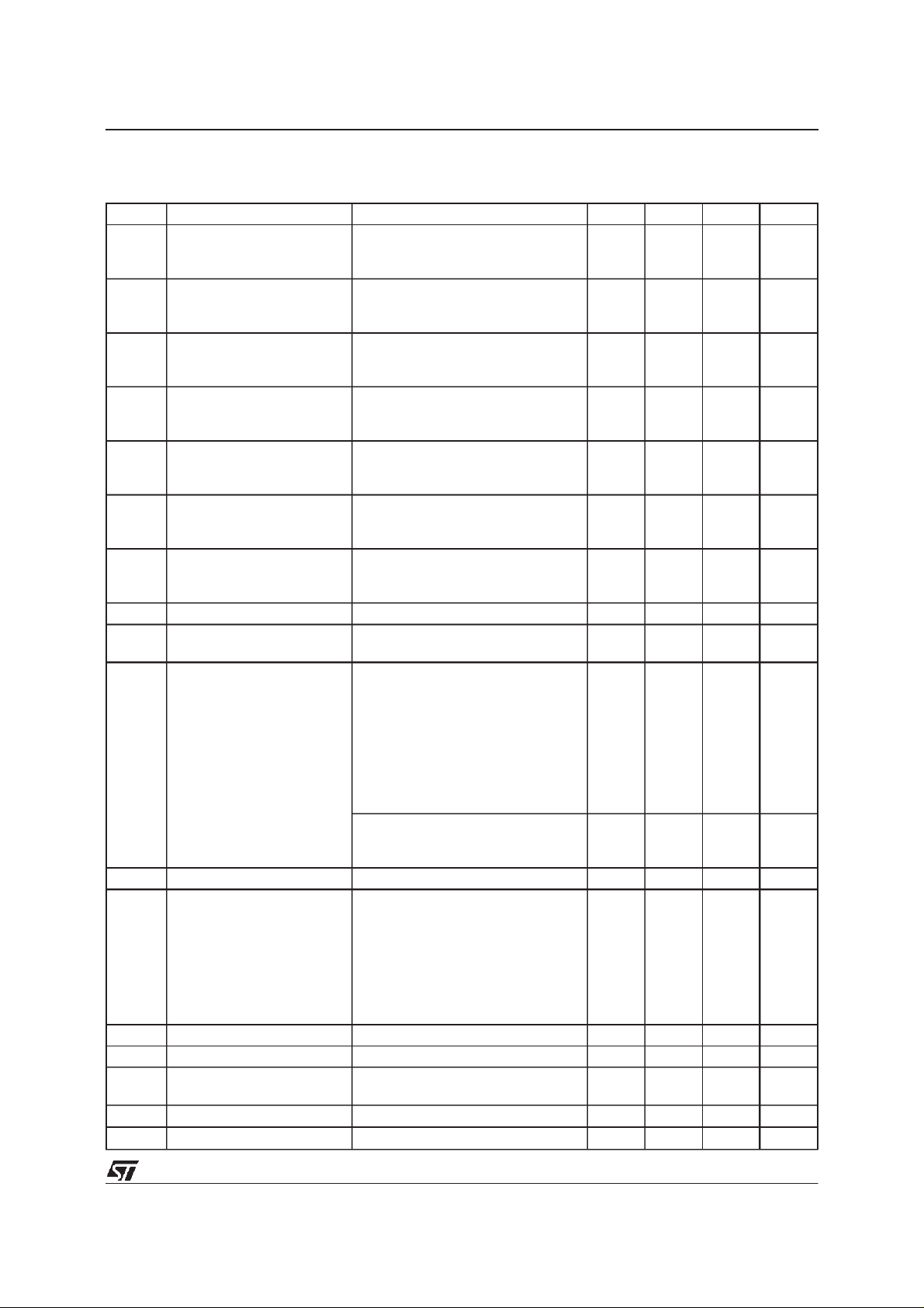
CONNECTION DIAGRAM
(*) Inhibitpin is not internallypulled-up then it must notbe left floating.Disable the device whenconnected to GND or to a positive voltage
less than 0.18V
(topview)
SOT23-5L
SOT-89
ORDERING NUMBERS
AB VERSION C VERSION Output Voltage
SOT23-5L SOT-89 SOT23-5L SOT-89
LD2981ABM28TR
LD2981ABM30TR
LD2981ABM32TR
LD2981ABM33TR
LD2981ABM38TR
LD2981ABM48TR
LD2981ABM50TR
LD2981ABU28TR
LD2981ABU30TR
LD2981ABU32TR
LD2981ABU33TR
LD2981ABU38TR
LD2981ABU48TR
LD2981ABU50TR
LD2981CM28TR
LD2981CM30TR
LD2981CM32TR
LD2981CM33TR
LD2981CM38TR
LD2981CM48TR
LD2981CM50TR
LD2981CU28TR
LD2981CU30TR
LD2981CU32TR
LD2981CU33TR
LD2981CU38TR
LD2981CU48TR
LD2981CU50TR
2.85 V
3.0 V
3.2 V
3.3 V
3.8 V
4.85 V
5.0 V
APPLICATION CIRCUIT
2/12
Page 3
LD2981
ELECTRICALCHARACTERISTICS FOR LD2981AB
V
IN=VO(NOM)
+1, CO=1µF, IO= 1mA, V
= 2V, unless otherwise specified)
INH
(refer to the test circuits,T
=25oC,
J
Symbol Parameter Test Conditions Min. Typ. Max. Unit
OutputVoltage VIN=3.85 V
V
o
OutputVoltage VIN=4V
V
o
OutputVoltage VIN=4.2 V
V
o
OutputVoltage VIN=4.3 V
V
o
OutputVoltage VIN=4.8 V
V
o
OutputVoltage VIN=5.85 V
V
o
OutputVoltage VIN=6V
V
o
OutputCurrentLimit 150 mA
I
out
V
∆
LineRegulation V
o
I
QuiescentCurrent ON MODE
d
<100 mA
1<I
o
<100 mA, -40< TJ< 125oC
1<I
o
<100 mA
1<I
o
<100 mA, -40< TJ< 125oC
1<I
o
<100 mA
1<I
o
<100 mA, -40< TJ< 125oC
1<I
o
1<I
<100 mA,
o
<100 mA, -40< TJ< 125oC
1<I
o
<100 mA,
1<I
o
1<I
<100 mA, -40< TJ< 125oC
o
<100 mA,
1<I
o
<100 mA, -40< TJ< 125oC
1<I
o
<100 mA,
1<I
o
<100 mA, -40< TJ< 125oC
1<I
o
+1< VIN<16V, Io=1mA
O(NOM)
-40 < T
I
I
I
I
I
I
I
I
< 125oC
J
=0mA
o
=0 mA -40 <TJ< 125oC
o
=1mA
o
=1 mA -40 <TJ< 125oC
o
=25mA
o
=25 mA -40< TJ<125oC
o
=100 mA
o
=100 mA -40< TJ<125oC
o
2.828
2.822
2.779
2.977
2.970
2.925
3.176
3.168
3.12
3.275
3.267
3.217
3.771
3.762
3.705
4.813
4.801
4.729
4.962
4.950
4.875
2.85 2.872
2.878
2.921
33.023
3.030
3.075
3.2 3. 224
3.232
3.28
3.3 3. 325
3.333
3.383
3.8 3. 829
3.838
3.895
4.85 4.887
4.899
4.971
55.038
5.050
5.125
0.003 0.014
0.032
80
100
150
100
150
200
250
400
800
800
1300
2600
%/V
OFF MODE
<0.3 V
V
INH
<0.15 V -40 < TJ< 125oC
V
INH
SVR Supply Voltage Rejection f = 1KHz, C
DropoutVoltage Io=0mA
V
d
ControlInput LogicLow LOW = OutputOFF -40< TJ<125oC0.18V
V
il
ControlInput LogicHigh HIGH = Output ON -40< TJ<125oC2 V
V
ih
ControlInput Current V
I
i
=0 mA -40 <TJ< 125oC
I
o
=1mA
I
o
=1 mA -40 <TJ< 125oC
I
o
=25mA
I
o
=25 mA -40< TJ<125oC
I
o
=100 mA
I
o
=100 mA -40< TJ<125oC
I
o
=0 V , -40< TJ<125oC
INH
=5 V, -40< TJ<125oC
V
INH
=10µF63dB
out
eN OutputNoise Voltage(RMS) BW = 300Hz to50 KHz, C
ShortCircuitCurrent RL=0 150 mA
I
SC
1
7
70
200
0
5
=10µF160 µV
out
0.8
2
3
5
10
15
100
150
250
375
-1
15
V
V
V
V
V
V
V
V
V
V
V
V
V
V
V
V
V
V
V
V
V
µA
µ
µA
µ
µA
µ
µA
µ
µ
µA
mV
mV
mV
mV
mV
mV
mV
mV
µA
µ
in
A
A
A
A
A
A
3/12
Page 4
LD2981
ELECTRICALCHARACTERISTICS FOR LD2981C
V
IN=VO(NOM)
+1, CO=1µF, IO= 1mA, V
= 2V, unless otherwise specified)
INH
(refer to the test circuits,T
=25oC,
J
Symbol Parameter Test Conditions Min. Typ. Max. Unit
OutputVoltage VIN=3.85 V
V
o
OutputVoltage VIN=4V
V
o
OutputVoltage VIN=4.2 V
V
o
OutputVoltage VIN=4.3 V
V
o
OutputVoltage VIN=4.8 V
V
o
OutputVoltage VIN=5.85 V
V
o
OutputVoltage VIN=6V
V
o
OutputCurrentLimit 150 mA
I
out
V
∆
LineRegulation V
o
I
QuiescentCurrent ON MODE
d
<100 mA
1<I
o
<100 mA, -40< TJ< 125oC
1<I
o
<100 mA
1<I
o
<100 mA, -40< TJ< 125oC
1<I
o
<100 mA
1<I
o
<100 mA, -40< TJ< 125oC
1<I
o
1<I
<100 mA,
o
<100 mA, -40< TJ< 125oC
1<I
o
<100 mA,
1<I
o
1<I
<100 mA, -40< TJ< 125oC
o
<100 mA,
1<I
o
<100 mA, -40< TJ< 125oC
1<I
o
<100 mA,
1<I
o
<100 mA, -40< TJ< 125oC
1<I
o
+1< VIN<16V, Io=1mA
O(NOM)
-40 < T
I
I
I
I
I
I
I
I
< 125oC
J
=0mA
o
=0 mA -40 <TJ< 125oC
o
=1mA
o
=1 mA -40 <TJ< 125oC
o
=25mA
o
=25 mA -40< TJ<125oC
o
=100 mA
o
=100 mA -40< TJ<125oC
o
2.814
2.793
2.750
2.962
2.940
2.895
3.160
3.136
3.088
3.259
3.234
3.184
3.752
3.724
3.667
4.789
4.753
4.680
4.937
4.900
4.825
2.85 2.886
2.907
2.950
33.038
3.060
3.105
3.2 3. 240
3.264
3.312
3.3 3. 341
3.366
3.416
3.8 3. 848
3.876
3.933
4.85 4.911
4.947
5.020
55.063
5.100
5.175
0.003 0.014
0.032
80
100
150
100
150
200
250
400
800
800
1300
2600
%/V
OFF MODE
<0.3 V
V
INH
<0.15 V -40 < TJ< 125oC
V
INH
SVR Supply Voltage Rejection f = 1KHz, C
DropoutVoltage Io=0mA
V
d
ControlInput LogicLow LOW = OutputOFF -40< TJ<125oC0.18V
V
il
ControlInput LogicHigh HIGH = Output ON -40< TJ<125oC2 V
V
ih
ControlInput Current V
I
i
=0 mA -40 <TJ< 125oC
I
o
=1mA
I
o
=1 mA -40 <TJ< 125oC
I
o
=25mA
I
o
=25 mA -40< TJ<125oC
I
o
=100 mA
I
o
=100 mA -40< TJ<125oC
I
o
=0 V , -40< TJ<125oC
INH
=5 V, -40< TJ<125oC
V
INH
=10µF63dB
out
eN OutputNoise Voltage(RMS) BW = 300Hz to50 KHz, C
ShortCircuitCurrent RL=0 150 mA
I
SC
1
7
70
200
0
5
=10µF160 µV
out
0.8
2
3
5
10
15
100
150
250
375
-1
15
V
V
V
V
V
V
V
V
V
V
V
V
V
V
V
V
V
V
V
V
V
µA
µ
µA
µ
µA
µ
µA
µ
µ
µA
mV
mV
mV
mV
mV
mV
mV
mV
µA
µ
in
A
A
A
A
A
A
4/12
Page 5

LD2981
TYPICALPERFORMANCE CHARACTERISTICS
OutputVoltage vs Temperature
OutputVoltage vs Input Voltage
(unless otherwise specified T
OutputVoltage vs Temperature
OutputVoltage vs InputVoltage
=25oC, CIN=C
J
OUT
=1µF)
OutputVoltage vs Output Current
OutputVoltage vs OutputCurrent
5/12
Page 6

LD2981
TYPICALPERFORMANCE CHARACTERISTICS
Line Regulationvs Temperature
DropoutVoltagevs OutputCurrent
(continued)
Dropout Voltagevs Temperature
QuiescentCurrent vs Temperature
QuiescentCurrent vs Output Current
6/12
QuiescentCurrent vs Input Voltage
Page 7

LD2981
TYPICALPERFORMANCE CHARACTERISTICS
S.V.R.vs Frequency
S.V.R.vs Output Current
(continued)
S.V.R.vs Temperature
Stability
Short Circuit Current vs Droput Voltage
ReverseCurrentvs ReverseVoltage
7/12
Page 8

LD2981
TYPICALPERFORMANCE CHARACTERISTICS
OutputVoltage vs Inhibit Voltage
SupplyVoltage Rejectionat V
=2.85V SupplyVoltage Rejectionat V
OUT
(continued)
InhibitCurrent vs Temperature
OUT
=5V
VIN= 7.35±2.5V, I
=0.1A, f = 1KHz VIN=9±2.5V,I
OUT
Line TransientResponse
VIN= 4.75 to 5.25V,I
8/12
= 0.1A,CO=10µF (ESR=1Ω at 1KHz) VIN= 4.75 to 5.25V,I
OUT
= 0.1A, f = 1KHz
OUT
Line TransientResponse
= 0.1A,CO=10µF (ESR=1Ω at 1KHz)
OUT
Page 9

LD2981
TYPICALPERFORMANCE CHARACTERISTICS
LoadTransient Response
VCC= 5V, I
(ESR=1Ω at 1KHz)
= 1 to 100mA,CIN= 150nF C
OUT
OUT
=10µF
ShutdownTransient Response
(continued)
LoadTransient Response
= 5V, I
V
CC
(ESR=1Ω at 1KHz)
= 1 to100mA,CIN= 150nF C
OUT
OUT
=10µF
V
=5V, VIN= 6V, V
OUT
=0to5V,CIN=C
INH
=1µF (Tant.)
OUT
9/12
Page 10

LD2981
SOT-89 MECHANICAL DATA
DIM.
MIN. TYP. MAX. MIN. TYP. MAX.
A 1.4 1.6 55.1 63.0
B 0.44 0.56 17.3 22.0
B1 0.36 0.48 14.2 18.9
C 0.35 0.44 13.8 17.3
C1 0.35 0.44 13.8 17.3
D 4.4 4.6 173.2 181.1
D1 1.62 1.83 63.8 72.0
E 2.29 2.6 90.2 102.4
e 1.42 1.57 55.9 61.8
e1 2.92 3.07 115.0 120.9
H 3.94 4.25 155.1 167.3
L 0.89 1.2 35.0 47.2
mm mils
10/12
P025H
Page 11

SOT23-5L MECHANICAL DATA
LD2981
DIM.
MIN. TYP. MAX. MIN. TYP. MAX.
A 0.90 1.45 35.4 57.1
A1 0.00 0.15 0.0 5.9
A2 0.90 1.30 35.4 51.2
b 0.35 0.50 13.7 19.7
C 0.09 0.20 3.5 7.8
D 2.80 3.00 110.2 118.1
E 2.60 3.00 102.3 118.1
E1 1.50 1.75 59.0 68.8
L 0.35 0.55 13.7 21.6
e 0.95 37.4
e1 1.9 74.8
mm mils
11/12
Page 12

LD2981
Information furnished is believed to be accurate andreliable. However,STMicroelectronics assumes no responsibility for the consequences
of use of such information nor for any infringement of patents or other rights of third parties which may result from its use. No license is
granted by implicationor otherwise under any patent or patent rights of STMicroelectronics. Specification mentioned in thispublication are
subject tochange without notice. Thispublication supersedes andreplaces allinformationpreviously supplied. STMicroelectronics products
are not authorized for use as critical components in life support devices or systems withoutexpress written approval of STMicroelectronics.
The ST logo isa registered trademark of STMicroelectronics
2000 STMicroelectronics – Printedin Italy – AllRightsReserved
STMicroelectronics GROUP OF COMPANIES
Australia - Brazil - China - Finland -France -Germany - Hong Kong - India - Italy- Japan- Malaysia - Malta - Morocco
Singapore - Spain- Sweden - Switzerland - UnitedKingdom - U.S.A.
http://www.st.com
.
12/12
 Loading...