

Datasheet LD29300V90, LD29300V80, LD29300V50, LD29300V33, LD29300D2T90 Datasheet (SGS Thomson Microelectronics)
...Page 1
3A, VERY LOW DROP V OLTAGE REGULATORS
■ VERY LOW DROPOUT V OLTAGE (TYP. 0.4
AT 3A)
■ GUARANTEED OUTPUT CURRENT UP TO
3A
■ FIXED VOLTAGE WITH±1% TO LERANCE
AT 25°C
■ INTERNAL CURRENT AND THERM AL LIM IT
■ LOGIC C ONTROLLED ELECTRO NIC
SHUTDOWN AVAILABLE IN PPAK
DESCRIPTION
The LD29300 is a high current, high accuracy,
low-dropout voltage regulator series. T hes e
regulators feature 400mV dropout voltage and
very low ground current. Designed forhigh current
loads, these devices are also used in lower
current, ext remel y low dropout-critical systems,
where their tiny dropout voltage and ground
current val ues are important attributes. Typical
applications are in Power supp ly switching post
regulation, Series power supply for monitors,
Series power supplyforVCRs and TVs, Computer
Systems and Battery powered systems.
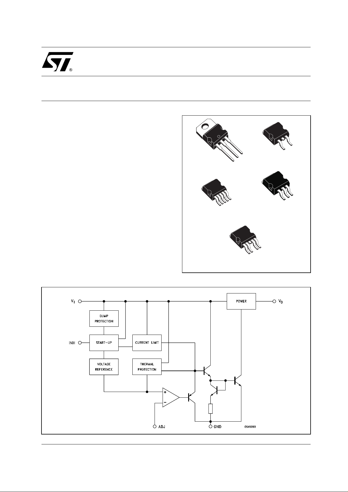
LD29300
SERIES
D2PAK
TO-220
D2PAK/A
P2PAK/A
P2PAK
SCHEMATIC DIAGRAM FOR ADJUSTABLE VERSION
1/17June 2003
Page 2
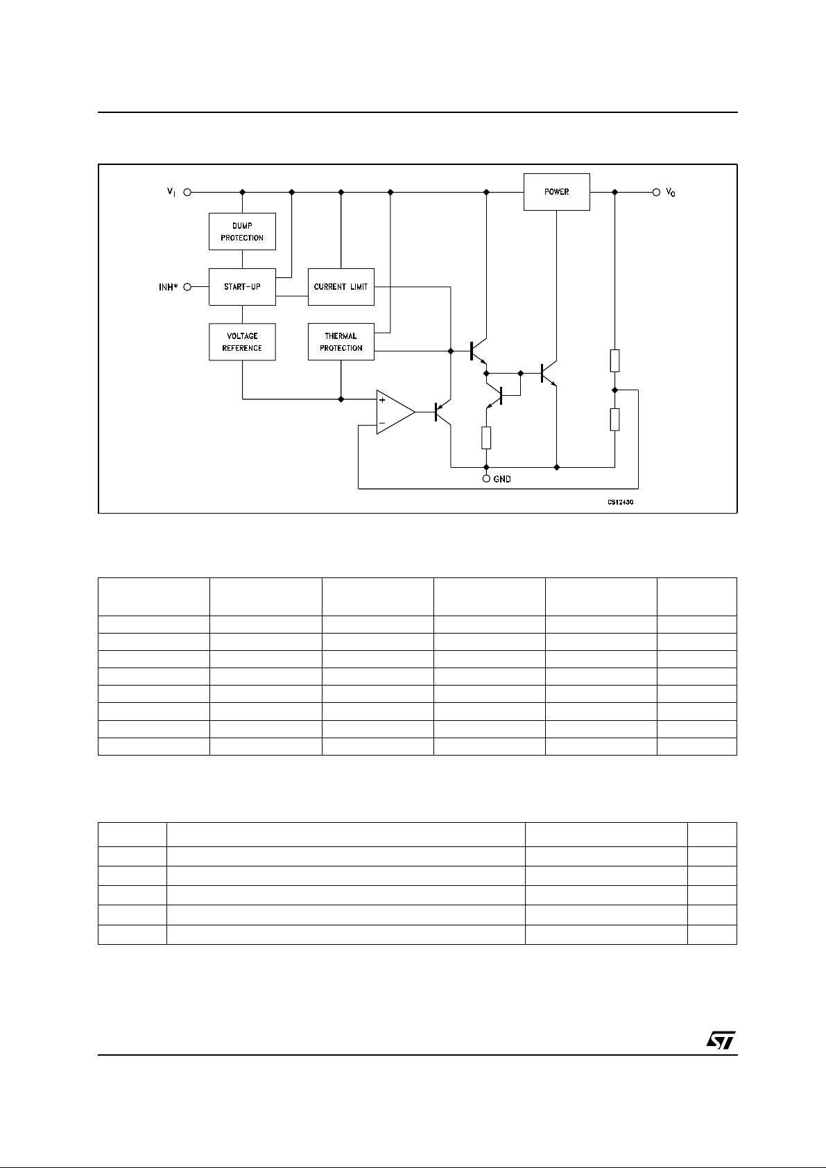
LD29300 SERIES
SCHEMATIC DIAGRAM FOR FIXED VERSION
* Only for version with inhibitfunction.
ORDERING CODES
TO-220
2
PAK (*) D2PAK/A (*) P2PAK (*)(#) P2PAK/A (*)
D
LD29300V15 LD29300D2T15 LD29300D2M15 LD29300P2T15 LD29300P2M15 1.5 V
LD29300V18 LD29300D2T18 LD29300D2M18 LD29300P2T18 LD29300P2M18 1.8 V
LD29300V25 LD29300D2T25 LD29300D2M25 LD29300P2T25 LD29300P2M25 2.5 V
LD29300V33 LD29300D2T33 LD29300D2M33 LD29300P2T33 LD29300P2M33 3.3 V
LD29300V50 LD29300D2T50 LD29300D2M50 LD29300P2T50 LD29300P2M50 5.0 V
LD29300V80 LD29300D2T80 LD29300D2M80 LD29300P2T80 LD29300P2M80 8.0 V
LD29300V90 LD29300D2T90 LD29300D2M90 LD29300P2T90 LD29300P2M90 9.0 V
LD29300P2T LD29300P2M ADJ
(*) Available in Tape & Reel with the suffix "R".
(#) Available on request.
OUTPUT
VOLTAGE
ABSOLUTE MAXIMUM RATINGS
Symbol Parameter Value Unit
V
I
P
T
T
(*) Above 14V the device is automaticallyin shut-down.
AbsoluteMaximumRatings are those beyond which damage to the device may occur. Functional operation under these condition is not implied.
DC Input Voltage
I
Output Current
O
Power Dissipation
D
Storage Temperature Range
stg
Operating Junction Temperature Range
op
30 (*) V
Internally Limited mA
Internally Limited mW
-55 to 150 °C
-40 to 125 °C
2/17
Page 3
THERMAL DATA
Symbol Parameter TO-220
R
thj-case
R
thj-amb
Thermal Resistance Junction-case
Thermal Resistance Junction-ambient
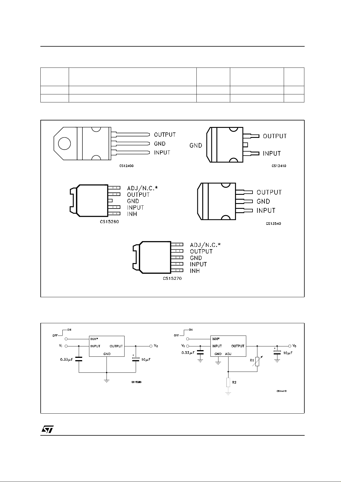
CONNECTION DIAGRAM (top view)
LD29300 SE RIE S
2
PAK-P2PAK
D
2
D
PAK/A-P2PAK/A
3 3 °C/W
50 60 °C/W
Unit
* Not connected for fixed version.
APPLICATION CIRCUIT
TO-220
D2PAK
P2PAK D2PAK/A
2
PAK/A
P
* Only for version with inhibitfunction.
VO=V
REF
R
1
(1 + )
R
2
3/17
Page 4
LD29300 SERIES
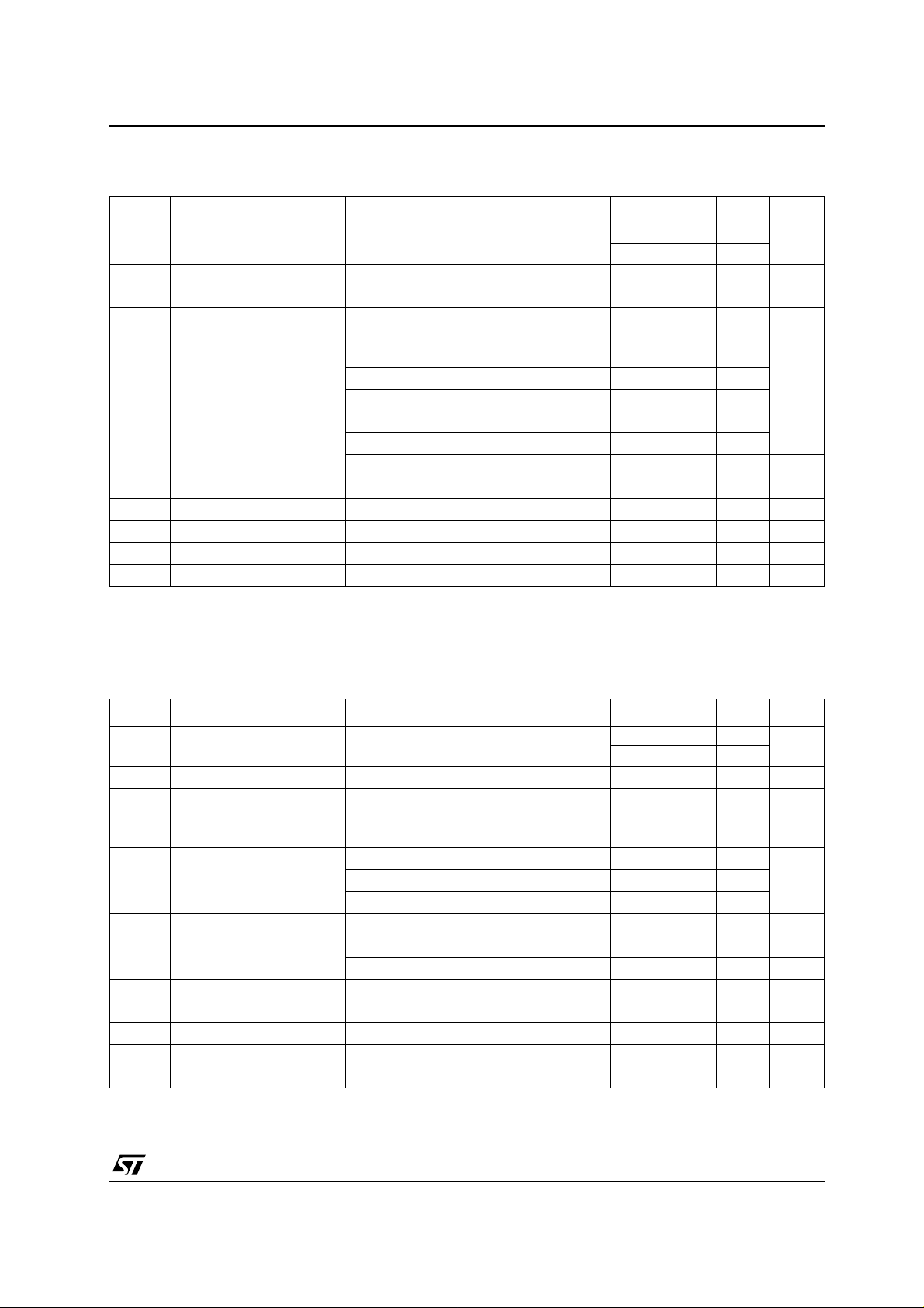
ELECTRICAL CHARACTERISTICS OF LD29300#15
(I
= 10mA, TJ=25°C,VI=3.5V,V
O
Symbol Parameter Test Conditions Min. Typ. Max. Unit
VIMinimum OperatingInput
Voltage
Output Voltage IO= 10mA to 3A, VI= 3 to 7V
V
O
∆V
∆V
Load Regulation IO= 10mA to 3A 0.2 1.0 %
O
Line Regulation VI= 3 to 13V 0.06 0.5 %
O
SVR Supply Voltage Rejection f = 120 Hz, V
Quiescent Current IO= 1.5A, TJ= -40 to 125°C 20 50 mA
I
q
Short Circuit Current VI-VO= 5.5V 4.5 A
I
sc
Control Input Logic Low OFF MODE, (NOTE 2) TJ= -40 to 125 °C 0.8 V
V
IL
Control Input Logic High ON MODE, (NOTE 2) TJ= -40 to 125 °C 2 V
V
IH
I
Control Input Current TJ= -40 to 125°C V
INH
eN O utput Noise Voltage B
NOTE 1: Guaranteed by design.
NOTE 2: Only for version with Inhibit function.
=2V(Note2),CI= 330nF, CO=10µF, unless otherwise specified)
INH
IO= 10mA to 3A
T
= -40 to 125°C
J
2.5 V
1.485 1.5 1.515 V
T
= -40 to 125°C
J
= 3.5 ± 1V, IO= 1.5A
I
1.47 1.53
65 75 dB
(Note 1)
= 3A, TJ= -40 to 125°C 45 100
I
O
= 13V, V
V
I
= 10Hz to 100KHz IO= 100mA 60 µV
P
=GND TJ= -40 to 125°C 130 180 µA
INH
= 13V 5 10 µA
INH
RMS
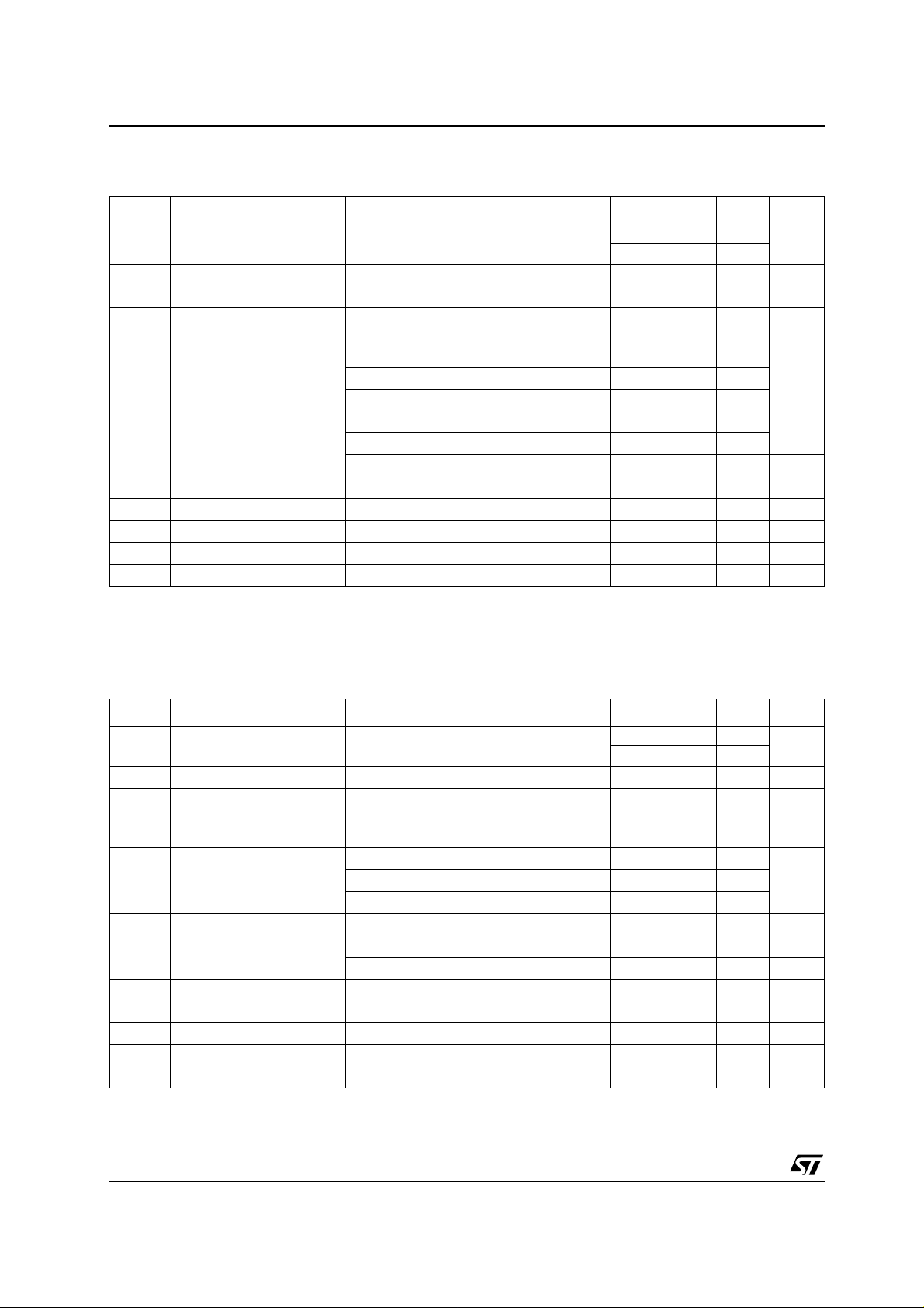
ELECTRICAL CHARACTERISTICS OF LD29300#18
(I
= 10mA,TJ= 25°C,VI=3.8V,V
O
Symbol Parameter Test Conditions Min. Typ. Max. Unit
Output Voltage IO= 10mA to 3A, VI= 3 to 7.3V
V
O
∆V
∆V
Load Regulation IO= 10mA to 3A 0.2 1.0 %
O
Line Regulation VI= 3 to 13V 0.06 0.5 %
O
SVR Supply Voltage Rejection f = 120 Hz, V
V
Dropout Voltage IO= 500mA, TJ= -40 to 125°C (Note 2) 0.1 V
DROP
Quiescent Current IO= 1.5A, TJ= -40 to 125°C 20 50 mA
I
q
Short Circuit Current VI-VO= 5.5V 4.5 A
I
sc
Control Input Logic Low OFF MODE, (NOTE 3) TJ= -40 to 125 °C 0.8 V
V
IL
Control Input Logic High ON MODE, (NOTE 3) TJ= -40 to 125 °C 2 V
V
IH
Control Input Current TJ= -40 to 125°C V
I
INH
eN O utput Noise Voltage B
NOTE 1: Guaranteed by design.
NOTE 2: Dropout voltageis defined asthe input-to-outputdifferential when the output voltage dropsto 99% of its nominal valuewith V
applied to VI.
NOTE 3: Only for version with Inhibit function.
=2V(Note3),CI= 330nF,CO=10µF, unless otherwisespecified)
INH
1.782 1.8 1.818 V
T
= -40 to 125°C
J
= 3.8 ± 1V, IO= 1.5A
I
1.764 1.836
62 72 dB
(Note 1)
= 1.5A, TJ= -40 to 125°C (Note 2) 0.2
I
O
= 3A, TJ= -40 to 125°C (Note 2) 0.4 0.7
I
O
= 3A, TJ= -40 to 125°C 45 100
I
O
= 13V, V
V
I
= 10Hz to 100KHz IO= 100mA 60 µV
P
=GND TJ= -40 to 125°C 130 180 µA
INH
= 13V 5 10 µA
INH
RMS
+1V
O
4/17
Page 5
LD29300 SE RIE S
ELECTRICAL CHARACTERISTICS OF LD29300#25
(I
= 10mA,TJ= 25°C,VI=4.5V,V
O
Symbol Parameter Test Conditions Min. Typ. Max. Unit
V
Output Voltage IO= 10mA to 3A, VI= 3.5 to 8V
O
∆V
∆V
Load Regulation IO= 10mA to 3A 0.2 1.0 %
O
Line Regulation VI= 3.5 to 13V 0.06 0.5 %
O
SVR Supply Voltage Rejection f = 120 Hz, V
V
Dropout Voltage IO= 500mA, TJ= -40 to 125°C (Note 2) 0.1 V
DROP
Quiescent Current IO= 1.5A, TJ= -40 to 125°C 20 50 mA
I
q
I
Short Circuit Current VI-VO= 5.5V 4.5 A
sc
Control Input Logic Low OFF MODE, (NOTE 3) TJ= -40 to 125 °C 0.8 V
V
IL
Control Input Logic High ON MODE, (NOTE 3) TJ= -40 to 125 °C 2 V
V
IH
Control Input Current TJ= -40 to 125°C V
I
INH
eN O utput Noise Voltage B
NOTE 1: Guaranteed by design.
NOTE 2: Dropout voltageis defined asthe input-to-outputdifferential when the output voltage dropsto 99% of its nominal valuewith VO+1V
applied to V
NOTE 3: Only for version with Inhibit function.
.
I
=2V(Note3),CI= 330nF,CO=10µF, unless otherwisespecified)
INH
2.475 2.5 2.525 V
T
= -40 to 125°C
J
= 4.5 ± 1V, IO= 1.5A
I
2.45 2.55
55 70 dB
(Note 1)
I
= 1.5A, TJ= -40 to 125°C (Note 2) 0.2
O
= 3A, TJ= -40 to 125°C (Note 2) 0.4 0.7
I
O
= 3A, TJ= -40 to 125°C 45 100
I
O
= 13V, V
V
I
= 10Hz to 100KHz IO= 100mA 100 µV
P
=GND TJ= -40 to 125°C 130 180 µA
INH
= 13V 5 10 µA
INH
RMS
ELECTRICAL CHARACTERISTICS OF LD29300#33
(I
= 10mA,TJ= 25°C,VI=5.3V,V
O
Symbol Parameter Test Conditions Min. Typ. Max. Unit
V
Output Voltage IO= 10mA to 3A, VI= 4.3 to 8.8V
O
∆V
∆V
Load Regulation IO= 10mA to 3A 0.2 1.0 %
O
Line Regulation VI= 4.3 to 13V 0.06 0.5 %
O
SVR Supply Voltage Rejection f = 120 Hz, V
V
Dropout Voltage IO= 500mA, TJ= -40 to 125°C (Note 2) 0.1 V
DROP
Quiescent Current IO= 1.5A, TJ= -40 to 125°C 20 50 mA
I
q
Short Circuit Current VI-VO= 5.5V 4.5 A
I
sc
Control Input Logic Low OFF MODE, (NOTE 3) TJ= -40 to 125 °C 0.8 V
V
IL
Control Input Logic High ON MODE, (NOTE 3) TJ= -40 to 125 °C 2 V
V
IH
Control Input Current TJ= -40 to 125°C V
I
INH
eN O utput Noise Voltage B
NOTE 1: Guaranteed by design.
NOTE 2: Dropout voltageis defined asthe input-to-outputdifferential when the output voltage dropsto 99% of its nominal valuewith V
applied to VI.
NOTE 3: Only for version with Inhibit function.
=2V(Note3),CI= 330nF,CO=10µF, unless otherwisespecified)
INH
3.267 3.3 3.333 V
T
= -40 to 125°C
J
= 5.3 ± 1V, IO= 1.5A
I
3.234 3.366
52 67 dB
(Note 1)
= 1.5A, TJ= -40 to 125°C (Note 2) 0.2
I
O
= 3A, TJ= -40 to 125°C (Note 2) 0.4 0.7
I
O
= 3A, TJ= -40 to 125°C 45 100
I
O
= 13V, V
V
I
= 10Hz to 100KHz IO= 100mA 132 µV
P
=GND TJ= -40 to 125°C 130 180 µA
INH
= 13V 5 10 µA
INH
RMS
+1V
O
5/17
Page 6
LD29300 SERIES
ELECTRICAL CHARACTERISTICS OF LD29300#50
(I
= 10mA, TJ=25°C,VI=7V,V
O
Symbol Parameter Test Conditions Min. Typ. Max. Unit
V
Output Voltage IO= 10mA to 3A, VI= 6 to 10.5V
O
∆V
∆V
Load Regulation IO= 10mA to 3A 0.2 1.0 %
O
Line Regulation VI= 6 to 13V 0.06 0.5 %
O
SVR Supply Voltage Rejection f = 120 Hz, V
V
Dropout Voltage IO= 500mA, TJ= -40 to 125°C (Note 2) 0.1 V
DROP
Quiescent Current IO= 1.5A, TJ= -40 to 125°C 20 50 mA
I
q
I
Short Circuit Current VI-VO= 5.5V 4.5 A
sc
Control Input Logic Low OFF MODE, (NOTE 3) TJ= -40 to 125°C 0.8 V
V
IL
Control Input Logic High ON MODE, (NOTE 3) TJ= -40 to 125°C 2 V
V
IH
Control Input Current TJ= -40 to 125°C V
I
INH
eN Output Noise Voltage B
NOTE 1: Guaranteed by design.
NOTE 2: Dropout voltageis defined asthe input-to-outputdifferential when the output voltage dropsto 99% of its nominal valuewith VO+1V
applied to V
NOTE 3: Only for version with Inhibit function.
.
I
=2V(Note3),CI= 330nF, CO=10µF, unless otherwise specified)
INH
4.95 5 5.05 V
T
= -40 to 125°C
J
=7 ± 1V, IO=1.5A
I
4.9 5.1
49 64 dB
(Note 1)
I
= 1.5A, TJ= -40 to 125°C (Note 2) 0.2
O
= 3A, TJ= -40 to 125°C (Note 2) 0.4 0.7
I
O
= 3A, TJ= -40 to 125°C 45 100
I
O
= 13V ,V
V
I
= 10Hz to 100KHz IO= 100mA 200 µV
P
=GND TJ= -40 to 125°C 130 180 µA
INH
= 13V 5 10 µA
INH
RMS
ELECTRICAL CHARACTERISTICS OF LD29300#80
(I
= 10mA, TJ= 25°C,VI=10V,V
O
Symbol Parameter Test Conditions Min. Typ. Max. Unit
V
Output Voltage IO= 10mA to 3A, VI= 9 to 13V
O
∆V
∆V
Load Regulation IO= 10mA to 3A 0.2 1.0 %
O
Line Regulation VI= 9 to 13V 0.06 0.5 %
O
SVR Supply Voltage Rejection f = 120 Hz, V
V
Dropout Voltage IO= 500mA, TJ= -40 to 125°C (Note 2) 0.1 V
DROP
Quiescent Current IO= 1.5A, TJ= -40 to 125°C 20 50 mA
I
q
Short Circuit Current VI-VO= 5.5V 4.5 A
I
sc
Control Input Logic Low OFF MODE, (NOTE 3) TJ= -40 to 125°C 0.8 V
V
IL
Control Input Logic High ON MODE, (NOTE 3) TJ= -40 to 125°C 2 V
V
IH
Control Input Current TJ= -40 to 125°C V
I
INH
eN Output Noise Voltage B
NOTE 1: Guaranteed by design.
NOTE 2: Dropout voltageis defined asthe input-to-outputdifferential when the output voltage dropsto 99% of its nominal valuewith V
applied to VI.
NOTE 3: Only for version with Inhibit function.
=2V(Note3),CI= 330nF, CO=10µF, unless otherwisespec ified)
INH
7.92 8 8.08 V
T
= -40 to 125°C
J
=9 ± 1V, IO=1.5A
I
7.84 8.16
45 59 dB
(Note 1)
= 1.5A, TJ= -40 to 125°C (Note 2) 0.2
I
O
= 3A, TJ= -40 to 125°C (Note 2) 0.4 0.7
I
O
= 3A, TJ= -40 to 125°C 45 100
I
O
= 13V ,V
V
I
= 10Hz to 100KHz IO= 100mA 320 µV
P
=GND TJ= -40 to 125°C 130 180 µA
INH
= 13V 5 10 µA
INH
RMS
+1V
O
6/17
Page 7

LD29300 SE RIE S
ELECTRICAL CHARACTERISTICS OF LD29300#90
(I
= 10mA, TJ= 25°C,VI=11V,V
O
Symbol Parameter Test Conditions Min. Typ. Max. Unit
V
Output Voltage IO= 10mA to 3A, VI=10to13V
O
∆V
∆V
Load Regulation IO= 10mA to 3A 0.2 1.0 %
O
Line Regulation VI= 10 to 13V 0.06 0.5 %
O
SVR Supply Voltage Rejection f = 120 Hz, V
V
Dropout Voltage IO= 500mA, TJ= -40 to 125°C (Note 2) 0.1 V
DROP
Quiescent Current IO= 1.5A, TJ= -40 to 125°C 20 50 mA
I
q
I
Short Circuit Current VI-VO= 5.5V 4.5 A
sc
Control Input Logic Low OFF MODE, (NOTE 3) TJ= -40 to 125°C 0.8 V
V
IL
Control Input Logic High ON MODE, (NOTE 3) TJ= -40 to 125°C 2 V
V
IH
Control Input Current TJ= -40 to 125°C V
I
INH
eN Output Noise Voltage B
NOTE 1: Guaranteed by design.
NOTE 2: Dropout voltageis defined asthe input-to-outputdifferential when the output voltage dropsto 99% of its nominal valuewith V
applied to VI.
NOTE 3: Only for version with Inhibit function.
=2V(Note3),CI= 330nF, CO=10µF, unless otherwisespec ified)
INH
8.91 9 9.09 V
T
= -40 to 125°C
J
=11 ± 1V, IO= 1.5A
I
8.82 9.18
45 58 dB
(Note 1)
I
= 1.5A, TJ= -40 to 125°C (Note 2) 0.2
O
= 3A, TJ= -40 to 125°C (Note 2) 0.4 0.7
I
O
= 3A, TJ= -40 to 125°C 50 100
I
O
= 13V ,V
V
I
= 10Hz to 100KHz IO= 100mA 360 µV
P
=GND TJ= -40 to 125°C 130 180 µA
INH
= 13V 5 10 µA
INH
RMS
+1V
O
ELECTRICAL CHARACTERISTICS O F LD29300#ADJ
= 10mA, TJ= 25°C, VI=3.23V,V
(I
O
Symbol Parameter Test Conditions Min. Typ. Max. Unit
V
Minimum OperatingInput
I
Voltage
∆V
∆V
V
Load Regulation IO= 10mA to 3A 0.2 1.0 %
O
Line Regulation VI= 2.5 V to 13V 0.06 0.5 %
O
Reference Voltage IO= 10mA to 3A, VI= 2.5 to 4.5V
REF
SVR Supply Voltage Rejection f = 120 Hz, V
Quiescent Current IO= 1.5A, TJ= -40 to 125°C 20 50 mA
I
q
I
Adjust Pin Current TJ= -40 to 125°C (Note 1) 1 µA
ADJ
Short Circuit Current VI-VO= 5.5V 4.5 A
I
sc
Control Input Logic Low OFF MODE, (NOTE 3) TJ= -40 to 125°C 0.8 V
V
IL
Control Input Logic High ON MODE, (NOTE 3) TJ= -40 to 125°C 2 V
V
IH
Control Input Current TJ= -40 to 125°C V
I
INH
eN Output Noise Voltage B
NOTE 1: Guaranteed by design.
NOTE 2: Reference Voltage is measured between output and GND pin, with ADJ PIN tied to V
NOTE 3: Only for version with Inhibit function.
=2V(Note3),CI= 330nF, CO=10µF adjust pin tied to output)
INH
IO= 10mA to 3A
T
= -40 to 125°C
J
2.5 V
-1% 1.23 +1% V
T
= -40 to 125°C (Note 2)
J
= 3.23 ± 1V, IO= 1.5A
I
-2% +2%
65 75 dB
(Note 1)
= 3A, TJ= -40 to 125°C 45 100
I
O
= 13V ,V
V
I
= 10Hz to 100KHz IO= 100mA 50 µV
P
=GND TJ= -40 to 125°C 130 180 µA
INH
= 13V 5 10 µA
INH
.
OUT
RMS
7/17
Page 8

LD29300 SERIES
TYPICAL CHARAC TERISTICS
Figure1 : Output Voltage vs Temperature
Figure2 : Dro pout Voltage vs Temp eratu re
(CI= 330nF, CO=10µF)
Figure4 : Quiesc ent Current vs Output Current
Figure5 : Quiesc ent Current vs Output Current
Figure3 : Dro pout Voltage vs Output Current
8/17
Figure6 : Quiesc ent Current vs Supply Voltage
Page 9

LD29300 SE RIE S
V
I
V
C
F
Figure7 : Quiesc ent Current vs Temp eratu re
Figure8 : Quiesc ent Current vs Temp eratu re
Figure10 : Supply Voltage Rejection vs
Temperature
Figure11 : StabilityvsC
O
Figure9 : Short Circuit Current vs Temperature
Figure12 : Line Transient
=3.5 to5.5V,
I
LOAD
=10mA,
=2.5V,
O
=10µ
O
9/17
Page 10

LD29300 SERIES
V
I
V
C
F
Figure13 : Load Transient
=4.5V,
I
=10mAto3A,
O
=2.5V,
O
O
=47µ
10/17
Page 11

LD29300 SE RIE S
TO-220 MECHANICAL DAT
DIM.
A 4.40 4.60 0.173 0.181
C 1.23 1.32 0.048 0.051
D 2.40 2.72 0.094 0.107
D1 1.27 0.050
E 0.49 0.70 0.019 0.027
F 0.61 0.88 0.024 0.034
F1 1.14 1.70 0.044 0.067
F2 1.14 1.70 0.044 0.067
G 4.95 5.15 0.194 0.203
G1 2.4 2.7 0.094 0.106
H2 10.0 10.40 0.393 0.409
L2 16.4 0.645
L4 13.0 14.0 0.511 0.551
L5 2.65 2.95 0.104 0.116
L6 15.25 15.75 0.600 0.620
L7 6.2 6.6 0.244 0.260
L9 3.5 3.93 0.137 0.154
DIA. 3.75 3.85 0.147 0.151
MIN. TYP MAX. MIN. TYP. MAX.
mm. inch
A
P011C
11/17
Page 12

LD29300 SERIES
D2PAK MEC
mm. inch
DIM.
MIN. TYP MAX. MIN. TYP. MAX.
A 4.4 4.6 0.173 0.181
A1 2.49 2.69 0.098 0.106
A2 0.03 0.23 0.001 0.009
B 0.7 0.93 0.027 0.036
B2 1.14 1.7 0.044 0.067
C 0.45 0.6 0.017 0.023
C2 1.23 1.36 0.048 0.053
D 8.95 9.35 0.352 0.368
D1 8 0.315
E 10 10.4 0.393 0.409
E1 8.5 0.335
G 4.88 5.28 0.192 0.208
L 15 15.85 0.590 0.624
L2 1.27 1.4 0.050 0.055
L3 1.4 1.75 0.055 0.068
M 2.4 3.2 0.094 0.126
R 0.4 0.016
V2 0˚ 8˚ 0˚ 8˚
HANICAL DATA
12/17
P011P6G
Page 13

P2PAK MECHANICAL DATA
LD29300 SE RIE S
DIM.
MIN. TYP MAX. MIN. TYP. MAX.
A 4.30 4.80 0.169 0.188
A1 2.40 2.80 0.094 0.110
A2 0.03 0.23 0.001 0.009
b 0.80 1.05 0.031 0.041
c 0.45 0.60 0.017 0.023
c2 1.17 1.37 0.046 0.053
D 8.95 9.35 0.352 0.368
D2 8 0.315
E 10.00 10.40 0.393 0.409
E1 8.5 0.334 0.409
e 3.20 3.60 0.126 0.142
e1 6.60 7.00 0.260 0.275
L 13.70 14.50 0.539 0.571
L2 1.25 1.40 0.049 0.055
L3 0.90 1.70 0.035 0.067
L5 1.55 2.40 0.061 0.094
R 0.40 0.016
V2 0˚ 8˚ 0˚ 8˚
mm. inch
7226255/B
13/17
Page 14

LD29300 SERIES
D2PAK/A MECHA
mm. inch
DIM.
MIN. TYP MAX. MIN. TYP. MAX.
A 4.40 4.60 0.173 0.181
A1 2.49 2.69 0.098 0.106
B 0.7 0.93 0.027 0.036
B2 1.14 1.7 0.044 0.067
C 0.45 0.60 0.017 0.023
C2 1.21 1.36 0.047 0.053
D 8.95 9.35 0.352 0.368
E 10 10.4 0.393 0.409
G 4.88 5.28 0.192 0.208
L 15 15.85 0.590 0.106
NICAL DATA
L2 1.27 1.4 0.050 0.055
14/17
Page 15

P2PAK/A MECHANICAL DATA
LD29300 SE RIE S
DIM.
MIN. TYP MAX. MIN. TYP. MAX.
A 4.30 4.80 0.169 0.188
A2 0.03 0.23 0.001 0.009
C 1.17 1.37 0.046 0.053
D 2.40 2.80 0.094 0.110
D1 8.95 9.35 0.352 0.368
E 0.45 0.60 0.017 0.023
F 0.80 1.05 0.031 0.041
G 3.20 3.60 0.126 0.142
G1 6.60 7.00 0.260 0.275
H1 8.5 0.334 0.409
H2 10.00 10.40 0.393 0.409
L 15 15.85 0.590 0.624
L1 8 0.315
L2 1.27 1.40 0.050 0.055
M 2.4 3.2 0.094 0.126
R 0.40 0.016
V2 0˚ 8˚ 0˚ 8˚
mm. inch
7157127/A
15/17
Page 16

LD29300 SERIES
Tape & Reel D
DIM.
A 180 7.086
C 12.8 13.0 13.2 0.504 0.512 0.519
D 20.2 0.795
N 60 2.362
T 14.4 0.567
Ao 10.50 10.6 10.70 0.413 0.417 0.421
Bo 15.70 15.80 15.90 0.618 0.622 0.626
Ko 4.80 4.90 5.00 0.189 0.193 0.197
Po 3.9 4.0 4.1 0.153 0.157 0.161
P 11.9 12.0 12.1 0.468 0.472 0.476
2
PAK-P2PAK-D2PAK/A-P2PAK/A MECHANICAL DATA
mm. inch
MIN. TYP MAX. MIN. TYP. MAX.
16/17
Page 17

LD29300 SE RIE S
Information furnished is believed to be accurate and reliable. However, STMicroelectronics assumes no responsibility for the
consequences of use o f suc h inf ormat ion n or f or an y infr ingeme nt of paten ts or oth er ri gh ts of third part ies whic h may resul t f rom
its use. No license is granted by implication or otherwise under any patent or patent rights of STMicroelectronics. Specifications
mentioned in this publication are subject to change without notice. This publication supersedes and replaces all information
previously supplied. STMicroelectronics products are not authorized for use as critical components in life support devices or
systems without express written approval of STMicroelectronics.
Australia - Brazil - Canada - China - Finland - France - Germany - Hong Kong - India - Israel - Italy - Japan - Malaysia - Malta - Morocco
© The ST logo is a registered trademark of STMicroelectronics
© 2003 STMicroelectronics - Printed in Italy - All Rights Reserved
STMicroelectronics GROUP OF COMPANIES
Singapore - Spain - Sweden - Switzerland - United Kingdom - United States.
© http://www.st.com
17/17
 Loading...